Article

A Non-Isolated High Voltage Gain DC–DC Converter Suitable for Sustainable Energy Systems

by
Mamdouh L. Alghaythi
Department of Electrical Engineering, College of Engineering, Jouf University, Sakaka 72388, Saudi Arabia
Sustainability 2023, 15(15), 12058; https://doi.org/10.3390/su151512058
Submission received: 10 May 2023 / Revised: 14 July 2023 / Accepted: 30 July 2023 / Published: 7 August 2023

Abstract

:
A non-isolated high gain DC–DC converter with magnetic coupling and a VM circuit is proposed in this study. By the use of the appropriate coupled inductor turn ratio, the output voltage of the recommended topology can be raised. The VM circuit is used to boost the voltage gain even further as well as to clamp the voltage spike across the switch, which results in a lower voltage on the switch. As a result, a MOSFET switch with a lower ON-state resistance (RDS-ON) is used which, in turn, causes the conduction losses to be reduced and the entire system efficiency to be raised. Another advantage of the proposed structure is the ZCS of the diodes, which reduces the voltage drop losses caused by the regenerative diodes. The function modes analysis and the theoretical equations are accomplished. A comparison survey with other prior works is being developed to investigate the competency of the proposed converter. Based on this, the higher voltage gain and efficiency as well as the lower voltage stress on the semiconductors can be achieved by the proposed converter compared to the other converters. The effectiveness of the proposed converter is confirmed by the experimental results at a laboratory-scale operating under 150 V output voltage with a 96% efficiency at the 150 W full load and a 25 kHz switching frequency.

1. Introduction

Consumer demand for renewable energy sources has increased throughout the world [1]. The primary disadvantages of using fossil fuels include environmental issues, the greenhouse effect, and climate change. On the other hand, the scarcity of fossil fuels encourages people to develop utilization of green energy sources, such as PV, wind turbines, and fuel cells [2]. Photovoltaic sources are one of the essential methods for absorbing greener energy, accounting for most power generation among all renewable energy choices [3]. However, renewable energy output voltage and power levels are low and must be improved for many high-power applications [4]. As a result, a transformer-less high voltage gain DC–DC topology with excellent efficiency is used to boost the voltage and power rating of renewable energy sources [5]. The typical boost converter may provide a high output voltage at a high-duty cycle, which raises the maximum voltage across the semiconductors and reduces overall system efficiency [6,7]. Furthermore, the conventional boost converter cannot achieve high efficiency because passive components are incompatible with renewable systems [8]. One of the primary downsides of boost architectures is the reverse recovery of output diodes, which causes the converter to run at a high duty cycle. As a result, the generated losses increase, and an EMI problem exists [9,10]. Hence, non-isolated converters utilized in renewable applications should have a high voltage gain, decreased input current ripple, and lower semiconductor maximum voltage [11].

Research Literature

Many different sorts of studies have been conducted to create DC–DC structures with high voltage gains [12]. Transformer-less DC–DC topologies with magnetizing inductors are used to achieve high voltage gain with a more extended source voltage gain and at a reduced cost [13,14,15]. The coupled inductor functions as a transformer, increasing the output voltage by selecting the suitable turn ratio [16]. However, the presence of inductive components reduces the efficiency of designs based on coupled inductors at kilowatt power levels [17]. Magnetic coupling converters benefit from clamped circuits with soft switching capabilities for quick switching in ZVS and ZCS. Nevertheless, they increase the topology’s complexity and raises the converter’s price [18]. One method uses converters, integrated coupled inductors, and switched capacitors to give a high voltage gain with a lower maximum voltage throughout the semiconductor elements and a reduced input current [19,20]. However, the ripple intensity via the output voltage and input current is significant, as is the cost of these systems due to the large number of passive and active components used [21]. By including a diode–capacitor circuit, the converter presented in [22] may prepare a high voltage gain with a smaller maximum voltage across the switch. The diode–capacitor circuit raises the output voltage at high-duty cycles by requiring semiconductors with high voltage and current ratings. This converter is inefficient and is not suggested for high power usage [23]. The switching capacitor and boost structures are mixed to provide a high voltage conversion ratio. These structures’ advantages include decreased current ripple and EMI [24]. The basic disadvantage of these topologies is their high maximum voltage across the diodes and considerable switching losses [25]. There is a transformer-free interleaved DC–DC structure with a high voltage gain [26]. These topologies are defined by their high output voltage, minimal losses, and compact volume and dimension [27]. However, these topologies have several flaws, including a reverse recovery problem, a high ripple content throughout the switch current, a high peak voltage of the controllable switch, and substantial switching losses [28,29,30,31]. Table 1 briefly overviews transformer-less high gain DC–DC converters [32,33].
This paper recommends a transformer-less DC–DC boost converter for sustainable systems. The advantages of the proposed configuration can be summarized as follows:
  • Higher voltage gain in comparison with others in the literature by the use of a coupled inductor and a voltage multiplier circuit.
  • Reduced maximum voltage of the switch due to the existence of the voltage multiplier circuit used as a clamp unit.
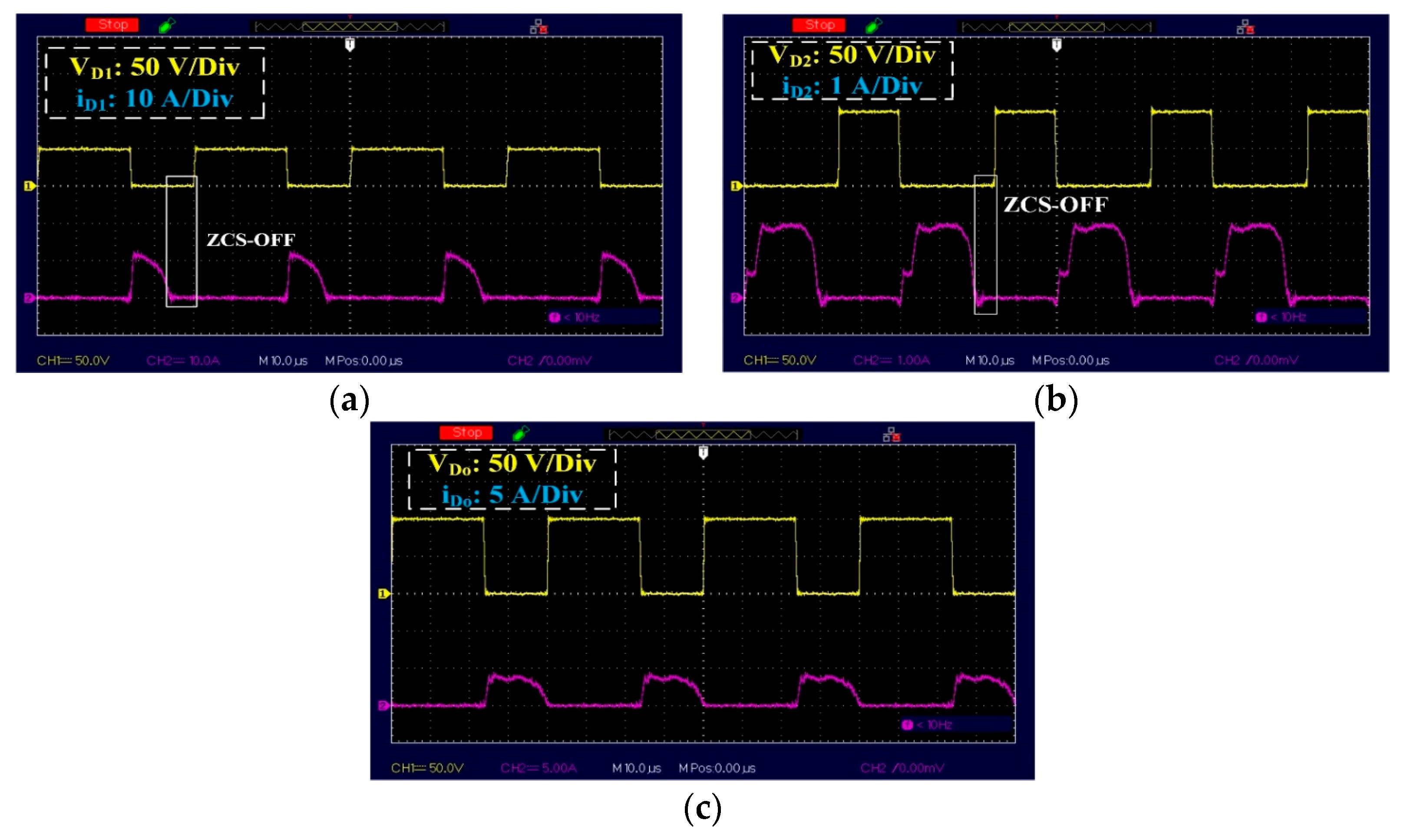
  • Operation of the diodes under ZCS, which reduces their reverse recovery losses.
  • Simple control system because of the one active switch used in the arrangement of the converter.
In the next sections, the proposed converter function in CCM is analyzed. Finally, a 150 W laboratory prototype at a 25 kHz switching frequency for 20 V input voltage and the 150 V output voltage is supplied to demonstrate the validity of the theoretical survey of the proposed topology. Table 2 lists the nomenclatures used in this paper.

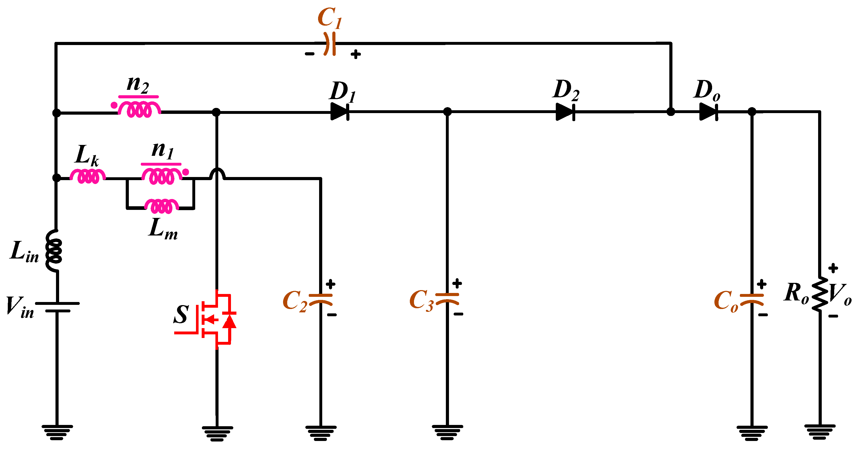
2. Material and Methods of Analysis the Proposed Converter

Figure 1 depicts the proposed prototype. This design includes a DC supply at the input, an input inductor (Lin), a magnetic coupling with two windings N1 (winding number of primary sides), and N2 (winding number of secondary sides), a VM circuit (consisting of a capacitor C2 and diodes D1, D2, an output diode (Do), and an output capacitor (Co)). It should be noted that the coupled inductor is modeled using an ideal transformer with two windings, namely magnetizing inductance (Lm) and leakage inductance (Lk). To have a simple analysis of the operation modes, the following suppositions are carried out:
  • The input DC source is consistent.
  • The calculations do not consider the elements’ ESR values (capacitors and inductors), diode ohmic losses, and active switch conducting resistance.
  • The intervals of transient state are ignored in the operating mode analysis.
  • The leakage inductor (Lk) has a small value and may be ignored during the operation.
The two time intervals occur during the one TS. The main switch is powered ON for (DTS), and the main switch is powered OFF for ((1 − D)TS).

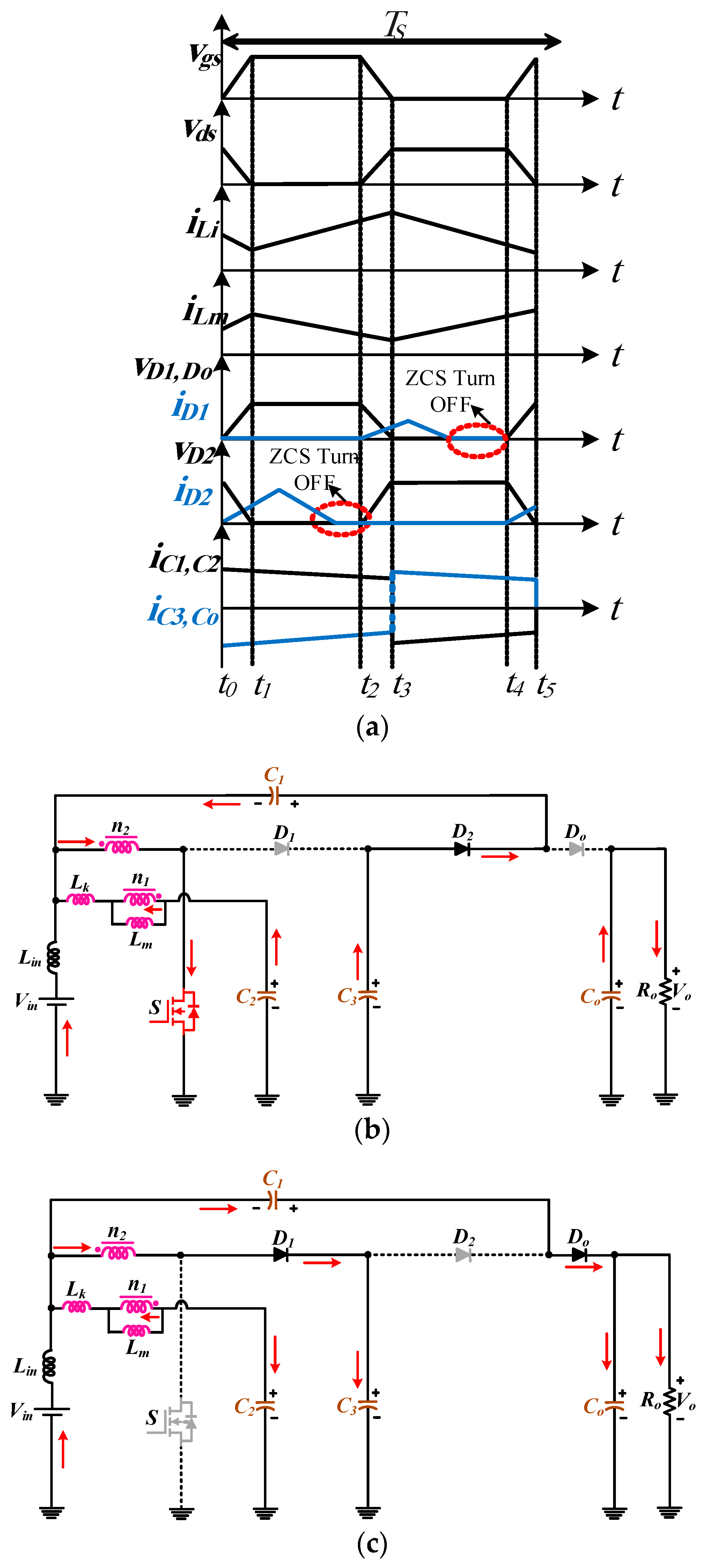
2.1. CCM Method Description

The basic waveforms, with their equivalent circuit of the suggested structure in CCM operation, have been indicated in Figure 2a–c, respectively. Thus, the following modes can be defined for CCM as follows:
Mode 1 [t0t1]: During this temporary period, the primary switch is in a conducting state at t = t1. Diodes D1 and Do are reverse-biased by the voltage VC3 and VoVC3, respectively. The energy from the input supply is transferred to Lin and the magnetic coupling.
Mode 2 [t1t2]: In this switching interval, the main switch is activated, and the diodes D1 and Do are in a reverse-biased state. Only diode D2 is conducting. As depicted in Figure 2a, diode D2 is switched off under the ZCS condition, effectively reducing the regenerative diode’s reverse recovery losses. The input inductor, Lin, and the secondary winding of the magnetic coupling inductor, Ln2, are charged by a DC power supply, causing the current, iLin, to increase linearly. Consequently, the stored energy in Ln2 charges the capacitors C1 and C2. During this phase, capacitor Co releases its energy to the load. The current flow path is depicted in Figure 2b. According to Figure 2b, the following Equations (1)–(3) can be derived in this switching operation:
V L i n = V i n + V C 1 V C 3
V L m = k ( V C 3 V C 2 V C 1 )
V n 2 = V C 3 V C 1
Mode 3 [t2t3]: During this transient switching period, the primary switch is obstructed at t = t3, and diode D2 is blocked by the voltage Vsw. The accumulated energy stored in LT2 is transferred to the magnetizing inductor (Lm). The inherent recycling effect of Lk plays a crucial role in controlling the behavior of diode D2. Using this advantage, the diode current experiences a gradual decline during the OFF mode, confirming the presence of the ZCS condition.
Mode 4 [t3t4]: This time interval occurs when the main switch is deactivated and diode D2 is blocked. Diodes D1 and Do are conducting. It is worth noting that diode D1 undergoes turn-off under the ZCS condition within this interval. The magnetizing inductor current (iLm) rises linearly as it stores energy from the input inductor during the first mode. Ln2 discharges its energy, transferring it to C3, resulting in the charging of the capacitor C3. The filter capacitor, Co, charges by utilizing the reserved energy from both the input inductor and the coupled inductor. At this particular moment, the maximum voltage throughout the power switch is suppressed by VC3. The current flow path is demonstrated in Figure 2c. Related to this figure, Equations (4)–(6) are obtained as follows:
V L i n = V i + V C 1 V o
V L m = k ( V o V C 1 V C 2 )
V n 2 = V o V C 1 V C 3
Mode 5 [t4t5]: The power switch is turned on in t = t5. During this transition instant, diodes D2 and Do are blocked. The input source charges the input inductor and LT2.
Based on the voltage–second balance law, the inductor voltage is zero in one TS. Therefore, the capacitor voltages in (7)–(9) can be achieved by applying this law as follows:
V C 1 = ( D 1 ) 2 1 D V o + ( 2 D 1 ) 1 D V i n
V C 2 = V i n
V C 3 = V i n 1 D
It is clear that (Vn1/Vn2 = N). Therefore, using this ratio and the voltages in (7)–(9), the voltage gain in CCM operation (MCCM) can be given as the following Equation (10):
M C C M = V o V i n = 2 k N 1 ( k N 1 ) ( 1 D )
Based on (10), the current gain is determined as follows in Equation (11):
I i n I o = 2 k N 1 ( k N 1 ) ( 1 D )
By noticing the obtained voltages for capacitors in (7)–(9), the peak voltage on the semiconductors can be written as follows in Equations (12)–(14):
V S = V C 3 = k N 1 2 k N 1 V o
V D 1 = V S = k N 1 2 k N 1 V o
V D 2 = V D o = V o V C 3 = k N 2 k N 1 V o

2.2. Current Calculation Method of the Components

As demonstrated in Figure 2b, the basic switch is powered ON in the first switching time mode. Hence, the current relations of capacitors in (15)–(18) can be expressed in this mode as follows:
I C 1 o n = I n 1 + I n 2 I i n
I C 2 o n = I n 1
I C 3 o n = I C 1 o n
I C o o n = I o
Figure 2c shows that the active switch is powered OFF. Hence, the current of the capacitors can be given as follows in Equations (19)–(22):
I C 1 o f f = I n 1 + I n 2 I i n
I C 2 o f f = I n 1
I C 3 o f f = I n 2
I C o o f f = I C 1 o f f I o
By employing the ampere–second balance principle for the capacitors, and given that the average current of diodes is the same as the output current Io, the average current which flows through the capacitors in each operation mode is defined as follows in Equations (23) and (24):
I C 1 o n = I C 2 o n = I C 3 o n = I o D
I C 3 o f f = I C 1 o f f = I C 2 o f f = I o 1 D
By remarking that N = 2, the current through the coupled inductor primary and secondary winding, diodes, and switch is calculated as in the following Equations (25)–(29):
I n 1 = I C 2 o n = I o D
I S = I n 2 = 3 I o 1 D
I D 1 = I n 2 = 3 I o 1 D
I D 2 = I C 1 o n = I o D
I D o = I C 1 o f f = I o 1 D

2.3. Components Selection

Substituting VC1 and VC3 from (7) and (9) into (1), the required input inductor can be obtained as in the following Equation (30):
L i n = 2 D V i n f s Δ I i n
where ΔI is the ripple content throughout the inductor. The ripple content of the input current should be low in PV systems, increasing the life span of PV arrays. Based on the currents flowing through the capacitors in Equations (23) and (24), the capacitance of the capacitors C1, C2, C3, and Co can be expressed, as in the following Equations (31) and (32):
C 1 , 2 , 3 = I o f s Δ V C 1 , 2 , 3
C o = D I o f s Δ V C o
where ΔV is the voltage ripple throughout the capacitor, which is typically within the range of 5% to 10% of the average voltage. The value of the capacitors is selected to balance the load voltage, which is essential to decline the voltage ripple.

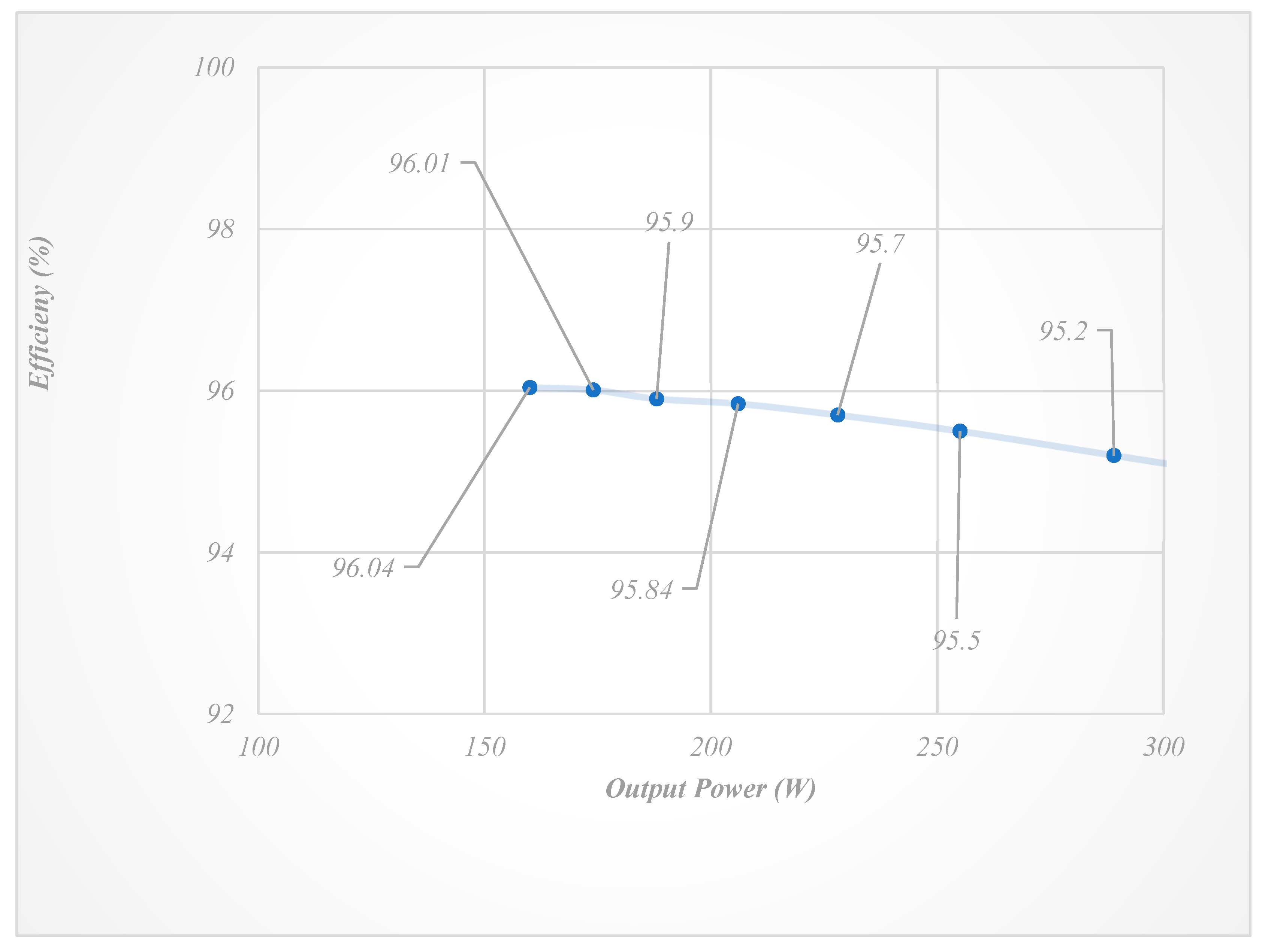
3. Efficiency Discussion of the Suggested Structure

This part presents the power losses and efficiency calculations of the suggested high step-up topology. The efficiency is expressed as in the following Equation (33):
E f f % = P o ( W ) P i n ( W ) × 100 % = P o ( W ) P i n ( W ) + P L o s s ( W ) × 100 %
Furthermore, the total power loss of the structure has been defined as Equation (34), which includes switch, diodes, magnetic devices, and capacitors loss, as follows:
P L o s s ( W ) = P L o s s S w i t c h + P L o s s D i o d e s + P L o s s M a g n e t i c + P L o s s c a p a c i t o r s
The power switch’s loss consists of switching and conducting losses, as follows in Equation (35):
P L o s s S w i t c h = P L o s s S w i t c h i n g + P L o s s C o n d u c t i n g = 1 2 ( t r i s e + t f a l l ) I S W a v g V S W f s + R d s ( O N ) ( I S W R M S ) 2
where trise and tfall are the rise and fall time during switching of the switch. Considering the ESR of elements, the total power loss of diodes, magnetic components, and capacitors can be obtained using the following Equations (36)–(38):
P L o s s D i o d e s = j = 1 N u m .   d i o d e s R d i o d e s ( O N ) j ( I S W j R M S ) 2
P L o s s M a g n e t i c = R E S R n 1 ( I n 1 R M S ) 2 + R E S R n 2 ( I n 2 R M S ) 2
P L o s s c a p a c i t o r s = j = 1 N u m . c a p a c i t o r R E S R C j I C j R M S 2

4. Reliability Discussion and Method

To show the proposed converter’s ability to respond to practical failures, the reliability analysis is provided based on [30]. The reliability study’s primary purpose is to quantify a power converter’s MTTF once it is incorporated through an application. As a reliability metric, MTTF is used to determine a system’s maximum life length. Also, it can be defined as the time until the first failure. The FR of the used elements in the converter’s circuit is evaluated to determine the MTTF. The probability function (r(t)) is described as not experiencing failure duration t, as follows [30]:
r ( t ) = e ( F R c o n v e r t e r   ×   t )
where F R c o n v e r t e r is the proposed converter’s failure rate. Also, MTTF is defined as (40) [30]:
M T T F = 0 r ( t ) d t = 1 F R c o n v e r t e r
where F R c o n v e r t e r includes the failure rates of semiconductors, inductors, and capacitors, as follows:
F R c o n v e r t e r = F R S w i t c h e s + F R D i o d e s + F R M a g n e t i c s + F R C a p a c i t o r s
The failure rate of the power switch S is attained as follows:
F R S w i t c h e s = l = 1 1 F R S j = j = 1 1 ( λ b j   π T j   π A j   π Q j   π E j )
And Tj is defined as in the following Equations (43) and (44):
π T _ S = e [ 1925 ( 1 T j   +   273 1 298 ) ]
T j = T a + R θ j A P L o s s _ S
The failure rate of diodes (D1, D2, and Do) is determined as follows:
F R D i o d e = l = 1 3 F R D j = j = 1 3 ( λ b j   π T j   π D j   π C j   π Q j   π E j )
Equations (46)–(48) are presented to determine the π D and π T of diodes, and TD, respectively.
π D = ( V D ) z
π T _ D = e [ 2100 ( 1 T D   +   273 1 298 ) ]
T D = R θ j A P L o s s _ D + T a
The magnetic components (input inductor and coupled inductor) failure rate can be obtained by the following Equation (49):
F R M a g n e t i c s = F R L i n + F R L C L = ( λ b L i n π T L i n π Q L i n π E L i n ) + ( λ b C L π T C L π Q C L π E C L )
where the π T of inductors, THS, and Δ T are defined as in the following Equations (50)–(52):
π T _ L = e [ 0.11 8.67   ×   10 5 ( 1 T H S   +   273 1 298 ) ]
T H S = T a + 1.2 Δ T
Δ T = 125 P L o s s _ L A L
Additionally, the failure rate of capacitors (C1, C2, C3, and Co) is calculated as follows:
λ C a p a c i t o r s = j = 1 4 λ C j = j = 1 4 ( λ b j   π T j   π V j   π C j   π Q j   π E j   π C a p j   π S R j )
π V = ( S C 0.6 ) n
π C a p = ( C   i n   μ F ) m
The temperature factor for capacitors can be reached by Equation (56), as follows:
π T _ C = e [ 0.35 8.67   ×   10 5 ( 1 T   +   273 1 298 ) ]
The content of the used parameters is presented in Table 3. The total FR of the suggested high step-up topology is determined as follows:
F R c o n v e r t e r = ( F R S w i t c h = 3.01 ) + ( F R D i o d e = 2.87 ) + ( F R M a g n e t i c = 1.92 ) + ( F R C a p a c i t o r = 1.56 )                                   = 9.36   f a i l u r e 1   million   hours λ c o n v e r t e r = 0.0819   f a i l u r e y e a r
Thus, MTTF is obtained as follows:
M T T F = 0 r ( t ) d t = 1 F R c o n v e r t e r = 12.21   y e a r s
It should be noticed that when increasing the converter’s rated power, current level, power losses, temperature, and failure rate are increased, which leads to lower reliability.

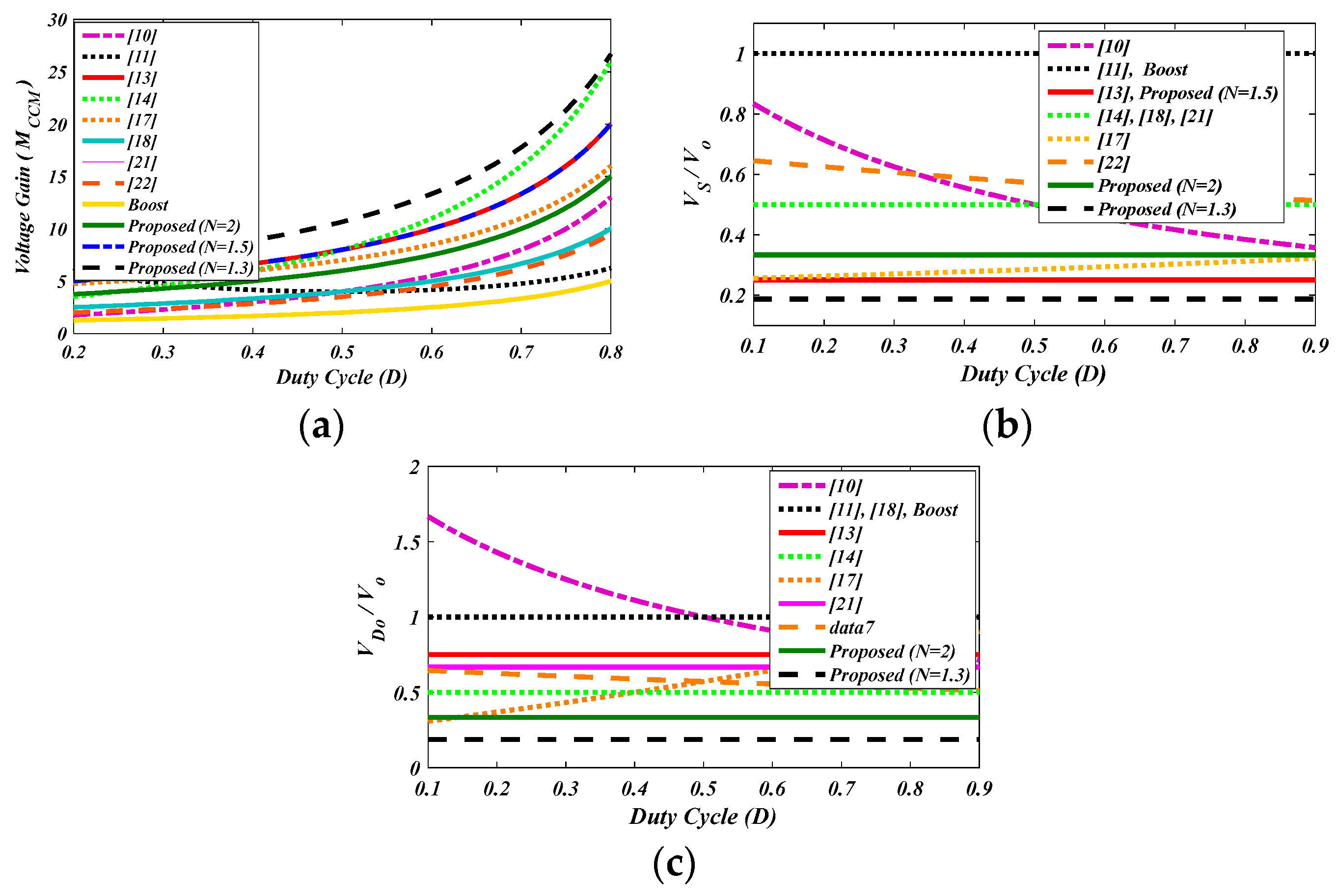
5. Discussion on the Feature Proposed Converter and Other Converters

Table 4 compares the proposed design to various prior topologies regarding voltage conversion ratio, maximum voltage across the switch (Mswitch), maximum voltage through the diode (Mdiode), component contents, soft switching capabilities, and efficiency. The given converter has a high voltage rate and fewer losses with a smaller maximum voltage throughout the semiconductors, making it suitable for renewable applications, such as solar. When the value of N is near 1, a high load voltage with a tiny peak voltage can be obtained across the diode and the switch. By reducing the value of N, the converter volume, the number of cores, and the cost of the proposed topology are reduced. Table 4 shows the proposed construction’s advantages and disadvantages compared to alternative converters. Figure 3a–c illustrates the voltage gain curve about the duty cycle, the maximum voltage of the switch about the duty cycle, and the maximum voltage throughout the diode about the duty cycle.
Table 4 shows the relationships between the presented structure voltage rate and duty cycle and existing converters (a). For all conversions, N = 2 is taken into account. Concerning Figure 3a, it is clear that the recommended topology has a higher load voltage ratio in comparison to the other topologies. The converters shown in [13,14] have a significant voltage gain, but their overall losses are substantial in contrast to the suggested converter, which is not recommended for use in high-power applications. The converter proposed in [18] can achieve high voltage conversion ratios with substantial losses, but it uses many components, raising the cost. Furthermore, the voltage rate of the given structure is higher when N and duty cycle are modest. As a result, the suggested structure may be used in various power level systems for quick, sustainable energy, LED drivers, and so on.
Figure 3 depicts the maximum voltage of the power switch curve dependent on the duty cycle (b). The peak voltage of the switch can be reduced by reducing the turn relation (for N > 1) of the magnetic coupling. As a result, just one switch with a lower resistance RDS-ON may be selected, resulting in lower conduction losses. The maximum voltage stress is high across the converters introduced in [10,14,18,21], necessitating a high-power switch at a high cost. However, by selecting an appropriate turn relation of the magnetic coupling (N), a converter with a high voltage ratio and a lower peak voltage across the switch may be given at a cheaper cost. As a result, the efficiency of the suggested converter can be raised.
As seen in Figure 3c, the suggested structure’s maximum voltage through the diode is low compared to alternative configurations. The voltage stress on the diode of the recommended converter is limited to 0.18 for N = 1.3, resulting in the usage of diodes with reduced voltage stress and cost. The peak voltage across the diode in the described converters [11,17,22] is high, and single switching is used in these architectures.

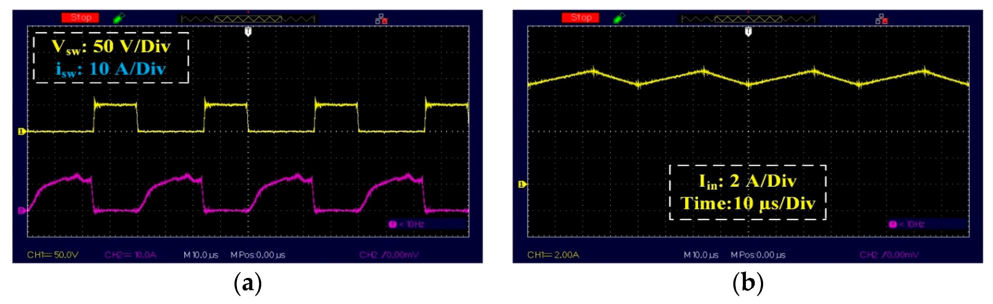
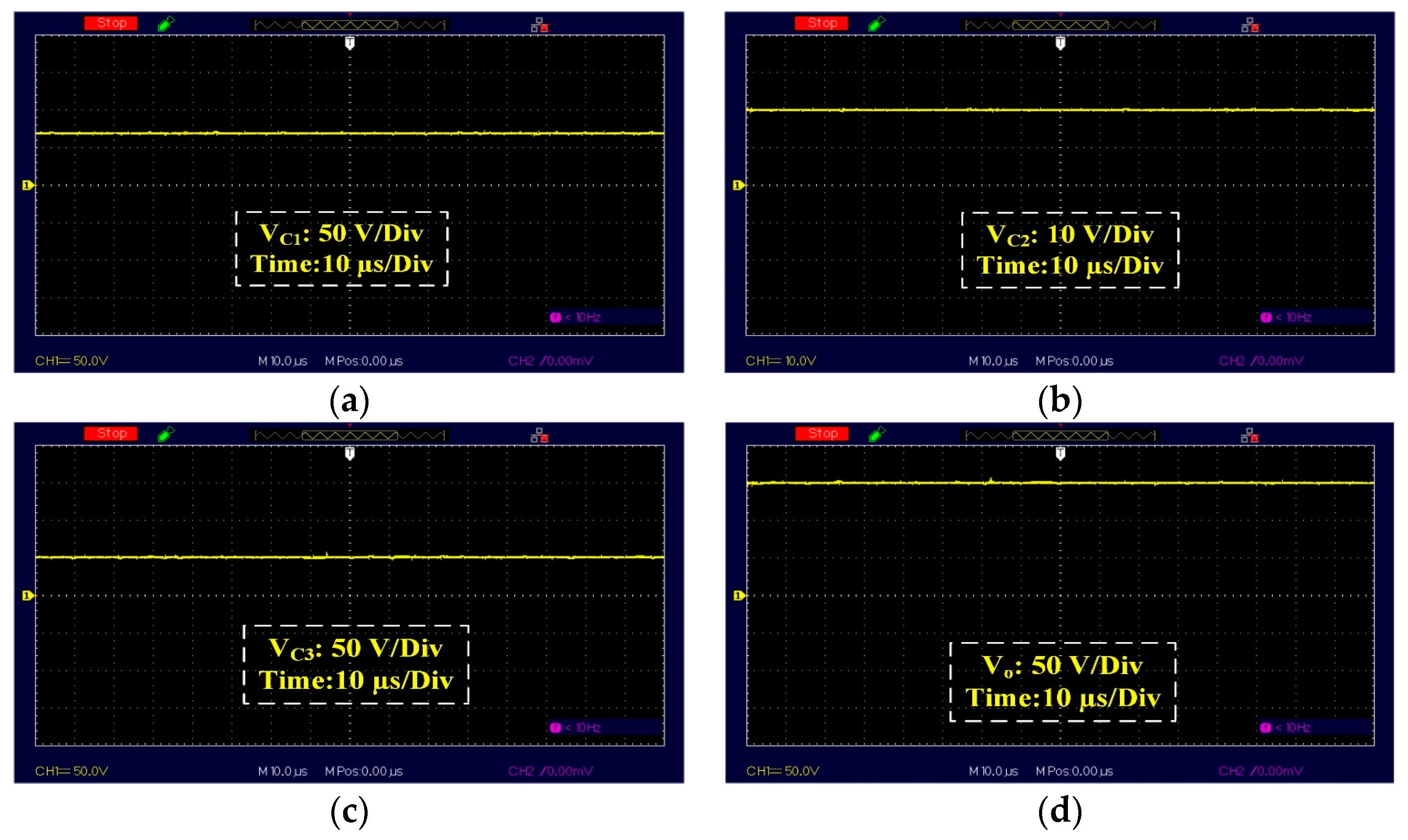
6. Result and Discussion

The laboratory verified the specified structure to corroborate the theoretical and mathematical analyses. Table 5 shows the essential specifications of the shown converter. The ATEMEGA16 microcontroller was used to control and generate the gate signal necessary to implement the given converter.
Figure 4, Figure 5 and Figure 6 show the experimental waveforms of the suggested topology in the CCM procedure. It should be noted that the recommended converter is written in D = 0.61 (duty-cycle). The primary switch’s OFF-state voltage waveform and drain-source current are shown in Figure 4a with a value of 51 V and 15 A, respectively. The peak voltage across the switch is far lower than the load voltage. The input current waveform is indicated in Figure 4b. In accordance with Figure 4b, the input side’s flowing current is continuous, extending the power supply’s lifetime. Furthermore, the input current ripple is about 8%, which is poor compared to the previous works. The diode’s voltage stress and current waveforms are illustrated in Figure 5a–c, respectively. According to Figure 5a, the peak voltage through the diode D1 is about 51 V, and also the iD1 = 12 A. According to Figure 5a, it is apparent that the diode D1 is switched off in the ZCS condition. The voltage and current waveform of diode D2 have been shown in Figure 5b, and the peak voltage throughout diode D2 is about 99 V. Related to Figure 5b, in the zero instant of the current, the diode turns off, confirming the ZCS condition for the proposed converter. According to Figure 5b, iD2 is about 2 A. Figure 5c depicts the voltage and current waveforms of the diode Do, which are about 99 V and 4.1 A, respectively. The output voltage and capacitors C1, C2, C3, and Co voltage waveforms are displayed in Figure 6a–d, respectively. Figure 6a illustrates that the value of the capacitor voltage C1 is about 69 V. In Figure 6b, VC2 is about 20 V. VC3 is approximately 51 V, as illustrated in Figure 6c. As displayed in Figure 6d, it can be noticed that the input voltage of the 20 V has increased to 150 V. From Figure 6d, it is also apparent that the output voltage ripple is very poor, and it can be ignored. The first and secondary side winding of the coupled inductor current have been shown in Figure 7a. From the technical survey and experimental tests, it is concluded that the laboratory waveforms verify the technical and mathematical formulas.
The theoretical analysis and findings show that the proposed structure is a viable option for green energy sources for instant PV panels (due to the low content of input current ripple and higher load voltage ratio). It may be utilized for varied power levels due to using a single power switch, lower peak voltage via the semiconductors, and higher voltage gain.
Figure 8 illustrates the efficiency curve for various power ratings, and Figure 9 illustrates an experimental prototype of proposed converter. The efficiency is controlled by taking into account parameters, such as N = 2, D = 0.61, and fs = 25 kHz. At an input voltage of 20 V and an output power of 150 W, the mentioned topology achieves a maximum efficiency of around 96%, as depicted in Figure 8. The overall load efficiency is approximately 95.2% at 300 W. It is apparent that the efficiency of the recommended topology exhibits a narrow margin when the load fluctuates between 150 W and 300 W. Hence, the overall efficiency of the suggested topology at all power levels is greater than 95%, which is recommended for sustainable utilization for instant PV generation.

7. Conclusions

This paper suggested a transformer-less DC–DC converter suitable for sustainable energy systems. According to the mathematical analysis and comparison survey, the contributions of this research can be presented as follows:
  • A coupled inductor-based DC–DC converter with higher voltage gains in comparison with other topologies in the literature. As a result, the proposed converter can achieve higher voltage gains with smaller values of the duty cycles than others.
  • Simple control system of the converter thanks to the existence of one switch.
  • Reduced input current ripple, which can increase the lifetime of the used input source, such as a PV or a battery.
  • Operation of the diodes under ZCS conditions reduces the reverse recovery losses of the regenerative diode.
  • The lower peak voltage on the switch makes it possible to select a MOSFET switch with a lower nominal voltage which, in turn, can reduce the conduction and switching losses.
Finally, an experimental prototype with a power level of 150 W was implemented to validate the effectiveness of the suggested structure. The experimental results stated that the proposed converter can operate under the 150 V output voltage with an efficiency of 96% at full load. In general, the described structure may be a suitable option for energy conversion applications, such as PV power production and fuel cells.
Despite the advantages mentioned above, this converter has some limitations that can be the basis for further research. In this converter, the soft switching operation has not been provided. Furthermore, the bidirectional power flow in which the power can be transferred from the output to the input, or a storage system can be added.

Funding

This work was funded by the Deanship of Scientific Research at Jouf University under grant No. (DSR-2021-02-0302).

Institutional Review Board Statement

Not applicable.

Informed Consent Statement

Not applicable.

Data Availability Statement

Data available upon request.

Acknowledgments

The author extends his appreciation to the Deanship of Scientific Research at Jouf University for funding this research work under grant No. (DSR-2021-02-0302).

Conflicts of Interest

The author declares no conflict of interest.

References

  1. He, Y.; Sun, X.; Liu, S.; Wang, N. High step-up DC–DC converter using coupled inductor voltage multiplier cell and differential connection method. IET Power Electron. 2023, 16, 542–557. [Google Scholar] [CrossRef]
  2. Soltani SR, K.; Mostafaeipour, A.; Almutairi, K.; Dehshiri, S.J.H.; Dehshiri SS, H.; Techato, K. Predicting effect of floating photovoltaic power plant on water loss through surface evaporation for wastewater pond using artificial intelligence: A case study. Sustain. Energy Technol. Assess. 2022, 50, 101849. [Google Scholar]
  3. Yong, X.; Wu, Y.; Zhou, J.; Tao, Y.; Chen, W. Prospects and barriers analysis framework for the development of energy storage sharing. Sustain. Cities Soc. 2023, 89, 104368. [Google Scholar] [CrossRef]
  4. Hashemzadeh, S.M.; Marzang, V.; Pourjafar, S.; Hosseini, S.H. An ultra high step-up dual-input single-output DC–DC converter based on coupled inductor. IEEE Trans. Ind. Electron. 2021, 69, 11023–11034. [Google Scholar] [CrossRef]
  5. Wu, X.; Yang, M.; Zhou, M.; Zhang, Y.; Fu, J. A novel high-gain dc-dc converter applied in fuel cell vehicles. IEEE Trans. Veh. Technol. 2020, 69, 12763–12774. [Google Scholar] [CrossRef]
  6. Palleswari, Y.T.R. A Novel Hybrid High Gain DC-DC converter for Renewable Energy Applications. Int. J. Renew. Energy Res. (IJRER) 2022, 12, 88–96. [Google Scholar]
  7. Pourjafar, S.; Shayeghi, H.; Hashemzadeh, S.M.; Sedaghati, F.; Maalandish, M. A non-isolated high step-up DC–DC converter using magnetic coupling and voltage multiplier circuit. IET Power Electron. 2021, 14, 1637–1655. [Google Scholar] [CrossRef]
  8. Shayeghi, H.; Pourjafar, S.; Hashemzadeh, S.M.; Blaabjerg, F. A high efficiency soft-switched DC–DC converter with high voltage conversion ratio. Int. J. Circuit Theory Appl. 2021, 49, 244–266. [Google Scholar] [CrossRef]
  9. Rao, B.T.; De, D. Effective leakage energy recycling in high gain DC-DC converter with coupled inductor. IEEE Trans. Circuits Syst. II Express Briefs 2022, 69, 3284–3288. [Google Scholar]
  10. Naderi, A.; Abbaszadeh, K. High step-up DC–DC converter with input current ripple cancellation. IET Power Electron. 2016, 9, 2394–2403. [Google Scholar] [CrossRef]
  11. Pourjafar, S.; Sedaghati, F.; Shayeghi, H.; Maalandish, M. High step-up DC–DC converter with coupled inductor suitable for renewable applications. IET Power Electron. 2018, 12, 92–101. [Google Scholar] [CrossRef]
  12. Abkenar, P.P.; Samimi, M.H.; Marzoughi, A.; Samavatian, V.; Iman-Eini, H.; Naghibzadeh, Y. A highly reliable low-cost single-switch resonant dc–dc converter with high gain and low component count. IEEE Trans. Ind. Electron. 2022, 70, 2556–2565. [Google Scholar] [CrossRef]
  13. Yang, L.S.; Liang, T.J.; Lee, H.C.; Chen, J.F. Novel high step-up DC–DC converter with coupled-inductor and voltage-doubler circuits. IEEE Trans. Ind. Electron. 2011, 58, 4196–4206. [Google Scholar] [CrossRef]
  14. Siwakoti, Y.P.; Blaabjerg, F. Single switch no isolated ultra-step-up DC–DC converter with an integrated coupled inductor for high boost applications. IEEE Trans. Power Electron. 2017, 32, 8544–8558. [Google Scholar] [CrossRef]
  15. Shayeghi, H.; Pourjafar, S.; Hashemzadeh, S.M.; Sedaghati, F. A DC-DC Converter with High Voltage Conversion Ratio Recommended for Renewable Energy Application. J. Oper. Autom. Power Eng. 2022. [Google Scholar] [CrossRef]
  16. Siva, A.; Rajendran, V. A novel auxiliary unit based high gain DC-DC converter for solar PV system with MPPT control. Int. J. Power Electron. Drive Syst. 2022, 13, 2386. [Google Scholar]
  17. Malik, M.Z.; Tirth, V.; Ali, A.; Farooq, A.; Algahtani, A.; Verma, R.; Islam, S.; Irshad, K.; Abdalla, A.N. Efficient Topology for DC-DC Boost Converter Based on Charge Pump Capacitor for Renewable Energy System. Int. J. Photoenergy 2021, 2021, 6675720. [Google Scholar] [CrossRef]
  18. Alghaythi, M.L.; O’Connell, R.M.; Islam, N.E.; Khan, M.M.S.; Guerrero, J.M. A High Step-Up Interleaved DC–DC Converter with Voltage Multiplier and Coupled Inductors for Renewable Energy Systems. IEEE Access 2020, 8, 123165–123174. [Google Scholar] [CrossRef]
  19. Hashemzadeh, S.M.; Hosseini, S.H.; Babaei, E.; Sabahi, M. A soft switched high step-up DC-DC converter based on VMC and coupled inductor for photovoltaic energy applications. IET Renew. Power Gener. 2023, 17, 1583–1596. [Google Scholar] [CrossRef]
  20. Sri Revathi, B.; Joseph Samuel, V.; Mahalingam, P. High step-up DC-DC converter based on double self-lift switched-coupled-inductor. Int. J. Electron. 2023, 110, 686–707. [Google Scholar] [CrossRef]
  21. Saravanan, S.; Babu, N.R. Design and Development of Single Switch High Step-Up DC–DC Converter. IEEE J. Emerg. Sel. Top. Power Electron. 2018, 6, 855–863. [Google Scholar] [CrossRef]
  22. Malik, M.Z.; Farh, H.M.; Al-Shaalan, A.M.; Al-Shamma’a, A.A.; Alhelou, H.H. A novel single-input-multi-output converter for flexible-order power-distributive with MPPT capability. IEEE Access 2021, 9, 131020–131032. [Google Scholar] [CrossRef]
  23. Leyva-Ramos, J.; Mota-Varona, R.; Ortiz-Lopez, M.G.; Diaz-Saldierna, L.H.; Langarica-Cordoba, D. Control Strategy of a Quadratic Boost Converter With Voltage Multiplier Cell for High-Voltage Gain. IEEE J. Emerg. Sel. Top. Power Electron. 2017, 5, 1761–1770. [Google Scholar] [CrossRef]
  24. Baba, M.F.; Giridhar, A.V.; Narasimharaju, B.L. Active switched-capacitor based ultra-voltage gain quadratic boost DC-DC converters. Int. J. Circuit Theory Appl. 2023, 51, 1389–1416. [Google Scholar] [CrossRef]
  25. Maalandish, M.; Hosseini, S.H.; Ghasemzadeh, S.; Babaei, E.; Alishah, R.S.; Jalilzadeh, T. Six-phase interleaved boost dc/dc converter with high-voltage gain and reduced voltage stress. IET Power Electron. 2017, 10, 1904–1914. [Google Scholar] [CrossRef]
  26. Malik, M.Z.; Zhang, S.; Hong, Y.; Alwahkyan AR, A.Y.; Ali, A.; Farooq, A. A Coupled Inductor-Based Bidirectional DC-DC Converter with Step-Up Step-Down Operation for Electric Vehicle Applications. Int. Trans. Electr. Energy Syst. 2023, 2023, 9277881. [Google Scholar] [CrossRef]
  27. Nouri, T.; Hosseini, S.H.; Babaei, E.; Ebrahimi, J. Interleaved high step-up DC–DC converter based on three-winding high-frequency coupled inductor and voltage multiplier cell. IET Power Electron. 2014, 8, 175–189. [Google Scholar] [CrossRef]
  28. Navauga, A.; Navamani, J.D.; Lavanya, A.; Vijayakumar, K. Comparison of high gain topologies of non-isolated dc-dc converters for fuel cell application. In Proceedings of the 2013 International Conference on Green Computing, Communication and Conservation of Energy (ICGCE), Chennai, India, 12–14 December 2013; pp. 367–372. [Google Scholar]
  29. Babu, K.V.; Vinay, K.S.; Chakraborty, P. Peer-to-Peer Sharing of Energy Storage Systems under Net Metering and Time-of-Use Pricing. IEEE Access 2023, 11, 3118–3128. [Google Scholar] [CrossRef]
  30. Alghaythi, M.L.; O’Connell, R.M.; Islam, N.E. Design of a High Step-up DC-DC Power Converter with Voltage Multiplier Cells and Reduced Losses on Semiconductors for Photovoltaic Systems. In Proceedings of the 2019 IEEE Electric Ship Technologies Symposium (ESTS), Arlington, VA, USA, 14–16 August 2019; pp. 214–218. [Google Scholar]
  31. Dehshiri, H.; Jalaladdin, S.; Amiri, M. An integrated multi-criteria decision-making framework under uncertainty for evaluating sustainable hydrogen production strategies based on renewable energies in Iran. Environ. Sci. Pollut. Res. 2023, 30, 46058–46073. [Google Scholar]
  32. Dehshiri, H.; Jalaladdin, S.; Zanjirchi, S.M. Comparative analysis of multicriteria decision-making approaches for evaluation hydrogen projects development from wind energy. Int. J. Energy Res. 2022, 46, 13356–13376. [Google Scholar] [CrossRef]
  33. Harms, J.W. Revision of MIL-HDBK-217, reliability prediction of electronic equipment. In Proceedings of the 2010 Proceedings-Annual Reliability and Maintainability Symposium (RAMS), San Jose, CA, USA, 25–28 January 2010; pp. 1–3. [Google Scholar]
Figure 1. Schematic of the suggested structure.
Sustainability 15 12058 g001
Figure 2. Key waveforms along with the equivalent circuits of the proposed topology in CCM operation. (a) Key waveforms, (b) equivalent circuit when the switch is powered ON, and (c) equivalent circuit when the switch is powered OFF.
Sustainability 15 12058 g002
Figure 3. Proposed structure comparison with other converters. (a) Voltage gain curve versus duty cycle, (b) peak voltage of the switch curve versus duty cycle, and (c) peak voltage of diode curve versus duty cycle.
Sustainability 15 12058 g003
Figure 4. The waveforms of the power switch and input current, (a) Drain-source voltage of the power switch (Vs), (b) Input current.
Sustainability 15 12058 g004
Figure 5. The voltage waveforms of the power diodes. (a) The voltage value of the power diode D1 (VD1), (b) the voltage value of the power diode D2 (VD2), and (c) the voltage value of the power diode Do (VDo).
Sustainability 15 12058 g005
Figure 6. The voltage waveforms of the capacitors. (a) VC1, (b) VC2 (c) VC3, and (d) VCo = Vo.
Sustainability 15 12058 g006
Figure 7. The current waveforms of the coupled inductor. (a) iLt2 and (b) iLt1.
Sustainability 15 12058 g007
Figure 8. The measured efficiency of the proposed converter based on various power loads.
Sustainability 15 12058 g008
Figure 9. The proposed converter prototype.
Sustainability 15 12058 g009
Table 1. Overview of non-isolated DC–DC structures with high voltage gain.
High Gain ConvertersAdvantagesDisadvantages
High gain DC–DC structure with magnetic couplingThe extended input voltage, low priceIn kilowatt levels, the efficiency is low (due to inductive elements)
High gain DC–DC structure with switched capacitorsHigh efficiencyHigh current stress of switches
High gain DC–DC structure with inductors and magnetizing inductorsLow peak voltage of the switch in comparison with the boost structure, high efficiencyHigh ripple of the input current and output voltage
High gain DC–DC structure with magnetic coupling and switching capacitorsLow maximum voltage on switchHigh ripple contents
High gain interleaved convertersLow input rippleLow output voltage rate, the high maximum voltage throughout the switch, high current ripple of the switch
Table 2. Nomenclature.
Abbreviation/VariableDescriptionAbbreviation/VariableDescription
DCDirect current λ b Base failure rate with a constant value
VMVoltage multiplier π A Application factor
PVPhotovoltaic π Q Quality factor
ZCSZero current switching π E Environmental factor
EMIElectromagnetic interference π T Temperature factor
ZVSZero voltage switching R θ j A Ambient thermal resistance
CCMContinuous conduction modeTaAmbient temperature
ESREquivalent series resistantPLoss_STotal power switches loss
MTTFMean time to failure π D Diodes voltage stress factor
FRFailure rate π C Diodes contact construction factor
TSSwitching period V D Applied voltage of diodes/rated voltage
DDuty cycleTHSHot spot temperature
Δ T Average rise in temperature π V Capacitors’ voltage stress factor
ALRadiating surface magnetic device’s area π C a p Capacitance factor
π S R Series resistance factorSCOperating voltage of capacitors/rated voltage
Table 3. Parameters utilized for reliability analysis.
ParameterValueParameterValue
λ b for switches0.012 π Q 8
λ b for diodes0.0038πE1
λ b for capacitors0.002 π C 1
λ b for magnetics0.004 π S R 1
Ta25 °CAL7
R θ j A for switches40.5 °C/Wz2.43
R θ j A for diodes62 °C/Wn3
πA8m0.23
Table 4. Comparison of the proposed converter features with other converters.
Converter[10][11][13][14][17][18][21][22]BoostProposed Converter
Voltage conversion ratio 1   +   N D 1     D 1 D ( 1     D ) N   +   2 1     D 1   +   N D 2 1     D 2   +   N     D 1     D N 1     D N   +   1 1     D 3   +   D 1     D 1 1     D 2 N     D 1     D
Mswitch 1 1   +   N D 1 1 N   +   2 0.5 1 2   +   N     D 1 N 1 N 2 3   +   D 1 N     1 2 N     1
Mdiode N 1   +   N D 1 N   +   1 N   +   2 0.5 1   +   N D 2   +   N     D 1 N N   +   1 2 3   +   D 1 N     1 2 N     1
No of Diodes2234241413
No of Switches1212113111
No of capacitors3232243414
No of inductors22-0-1-211
No of coupled inductors1-11111--1
Total devices no.9889611811410
Efficiency9494.292.592.893.696.29492.259096
Soft SwitchNoNoYesNoNoYesYesNo-Yes
Table 5. Specifications of the used elements.
ParameterSpecifications
Output Power (Po)150 W
Power supply voltage (Vin)20 V
Load voltage (Vo)150 V
Operation frequency of the switch (fs)25 kHz
Turn ratio of the coupled inductor N(N1/N2)2/1
Magnetizing inductance (Lm)250 µH
Input inductor (Lin)500 µ H
MOSFET (S)STW55NM60
DiodesRHRP15120
The used capacitors (C1, C2, C3)100 µF/220 V
Output capacitor (Co)470 µF/400 V
Disclaimer/Publisher’s Note: The statements, opinions and data contained in all publications are solely those of the individual author(s) and contributor(s) and not of MDPI and/or the editor(s). MDPI and/or the editor(s) disclaim responsibility for any injury to people or property resulting from any ideas, methods, instructions or products referred to in the content.

