Article

An Asymmetrical Step-Up Multilevel Inverter Based on Switched-Capacitor Network

1
School of Engineering, Deakin University, Geelong, VIC 3216, Australia
2
Faculty of Electrical and Computer Engineering, Babol Noshirvani University of Technology, Mazandaran 47148-71167, Iran
3
Intelligent Electrical Power Grids at Department of Electrical Sustainable Energy, Delft University of Technology, 5031, 2600 GA Delft, The Netherlands
4
Faculty of Engineering and Technology, University of Mazandaran, Babolsar 47416-13534, Iran
5
Department of System Engineering and Automatic Control, University of Seville, 41004 Seville, Spain
6
Department of Electrical Engineering and Automation, Aalto University, Maarintie 8, 02150 Espoo, Finland
*
Author to whom correspondence should be addressed.
Sustainability 2019, 11(12), 3453; https://doi.org/10.3390/su11123453
Submission received: 3 June 2019 / Revised: 17 June 2019 / Accepted: 17 June 2019 / Published: 23 June 2019
(This article belongs to the Special Issue Power Electronics for Renewable Energy Systems)

Abstract

:
This paper presents a transformerless step-up multilevel inverter based on a switched-capacitor structure. One of the main contributions of the proposed topology is replacing the separated DC voltage source with capacitors which are charged at predetermined time intervals. Therefore, a high-level staircase voltage waveform can be achieved by discharging some of these capacitors on the load. The other contribution of the proposed structure is to eliminate the magnetic elements which traditionally boost the input DC voltage. In addition, asymmetrical or unequal amounts of capacitor voltages create more voltage levels, which enable voltage level increments without increasing the number of semiconductor devices. This paper introduces a self-balanced boost Switched-Capacitors Multilevel Inverter (SCMLI) which is able to create a nearly sinusoidal voltage waveform with a maximum voltage of up to 45 times that of the input voltage DC source. Higher level output voltage levels are also achievable by extending the circuit topology. After determination of the switching angles and selecting the proper switching states for each level, an offline NLC method is used for modulation, which eases the control implementation. Analysis, simulation and experiments are carried out for a 91-level inverter (45 levels for positive and negative voltages and one for zero voltage) are presented.

1. Introduction

Multilevel inverters (MLIs) are widely used in high voltage high power applications such as renewable energy resources, HVDC systems, power industry, high power motor drives, and energy transmission systems [1]. The term “multi-level” was started with the three-level converter in 1981 by Nabae [2], and gradually expanded to higher levels. These converters include arrays of power semiconductors, capacitors and DC sources which generate a staircase voltage waveform through a proper pulse pattern. Neutral point clamped (NPC) and flying capacitor (FC) [3] are among the famous topologies of MLIs, which utilize different capacitors and switches to generate a staircase voltage waveform. Cascaded H-Bridge (CHB) topology is introduced for systems with multiple separate DC sources such as solar cell farms [4] and a single DC source [5].
Increasing the voltage levels improves output voltage quality but leads to an increment of switching devices and other components. This consequently causes complexity in the control and maintenance of such systems. Multilevel converters with asymmetrical or unequal DC sources are introduced to achieve higher voltage levels without increasing the number of circuit components [6,7]. In order to achieve higher voltage levels at the output, [8,9,10] new structures with fewer components and DC sources have been proposed. Different topologies for symmetric and asymmetric multilevel inverters are shown in [11], which summarizes recent improved topologies. For both symmetrical and asymmetrical topologies, multiple DC sources are required, which may not be available in all conditions [12]. Capacitors can be used in these structures but they also need additional circuits for voltage balancing. Therefore, a converter with the lowest possible number of DC sources and self-balanced capacitors is essential in order to achieve higher voltage levels with a reduced number of components [13]. On the other hand, low voltage DC input sources are used in many applications such as photovoltaic farms [14], electric vehicles [15] and battery applications [16]. Step-up DC-AC Power converters are required to generate voltage for AC loads or grid connection purposes. Traditionally, multi-stage power conversion is required to achieve the required voltage. A transformerless converter is required to convert low voltage DC to high output AC voltage at a single stage.
The authors of [17] presented a single source self-balanced SCMLI topology which uses two switches, two diodes and a capacitor to generate each voltage level. A bipolar MLI based on CHB structure is presented at [18] which consist of full bridge modules. These two topologies suffer from a large number of switching components and high voltage stress on switches. To overcome this limitation, [19] presented a modular SCMLI structure which consists of modules with three powers switches. The number of semiconductors decreased in [20,21] by improving this topology by replacing a diode instead of a switch, which causes a reduction of the number of required drivers as well. The structure proposed in [22] reduces the number of switches to one in each module, which leads to reducing drivers and ease of control in comparison with other topologies. However, the voltage stress on each of the switches increases by voltage level increment as well as increasing the number of series diodes. The authors of [23] presented another SCMLI to reduce voltage stress on the switches based on cascading different modules together. The main problem of this structure is the requirement of additional circuits for balancing purposes.
In this paper, the proposed topology solves the main issues of the mentioned topologies which are (i) the number of switching devices, and (ii) voltage stress on different components during level increment. Moreover, the proposed structure has the ability to boost the input voltage without using any magnetic elements, and can convert a low DC voltage to a high voltage AC output by using single DC source. The challenge of the number of components necessitates the presentation of a step up DC-AC MLI converter based on SC network with reduced number of circuit elements such as capacitors and power semiconductors. Charging the capacitors (up to multiples of input voltage) and smart discharging of several capacitors at predetermined periods enables the proposed topology to increase the number of voltage level steps and boost ratio of the converter. As the input voltage of the converter is low, the rating of components is kept within an acceptable range.
The next section of the paper explains the circuit topology and its modules. Topology operation such as switching states, mathematical analysis, modulation strategy, charging and discharging of capacitors are analyzed at Section 3. A circuit extension and a comparative study is carried out in Section 4. The analyses are validated by a simulation and experimental results in Section 5. A conclusion is presented in Section 6.

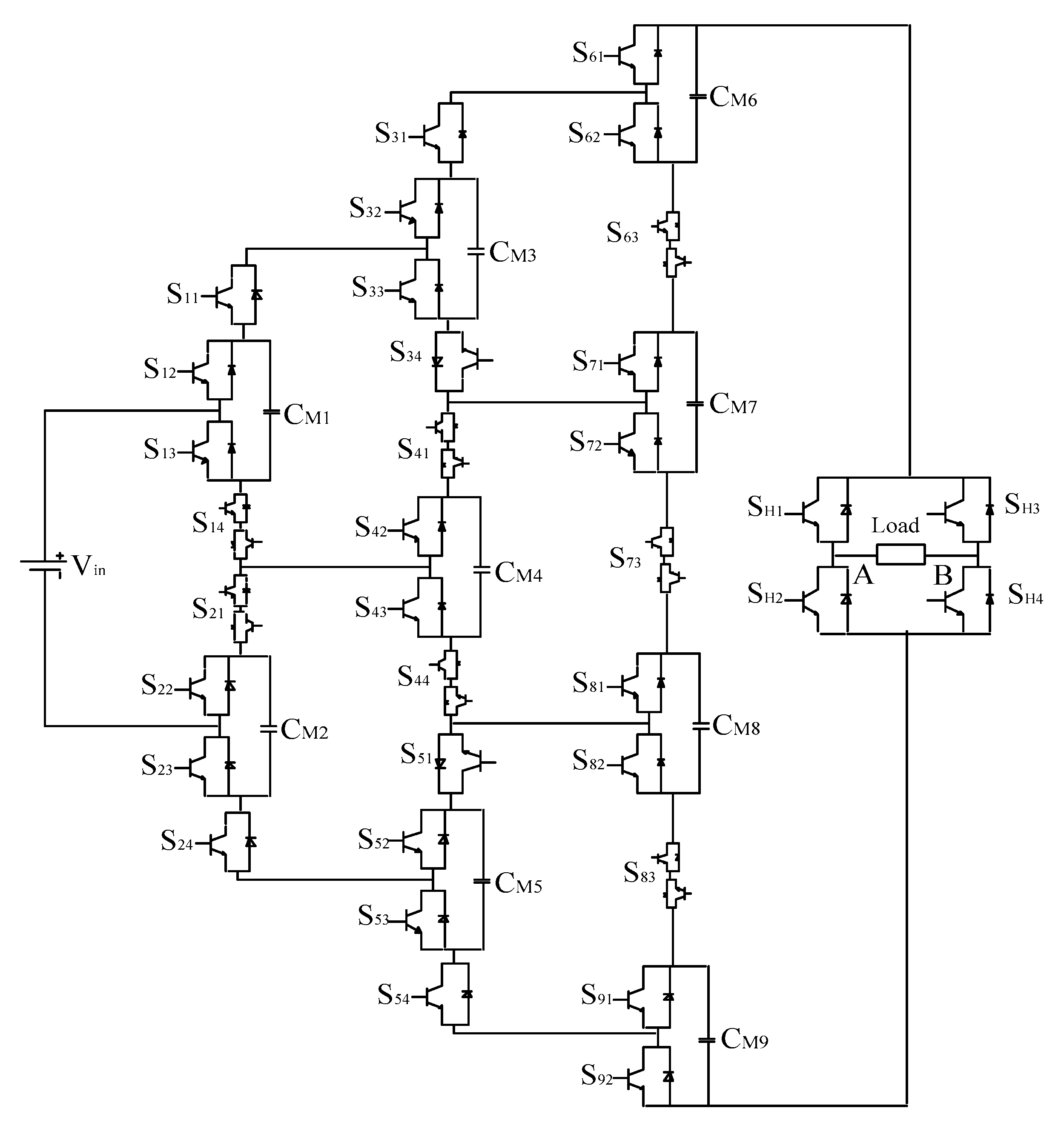
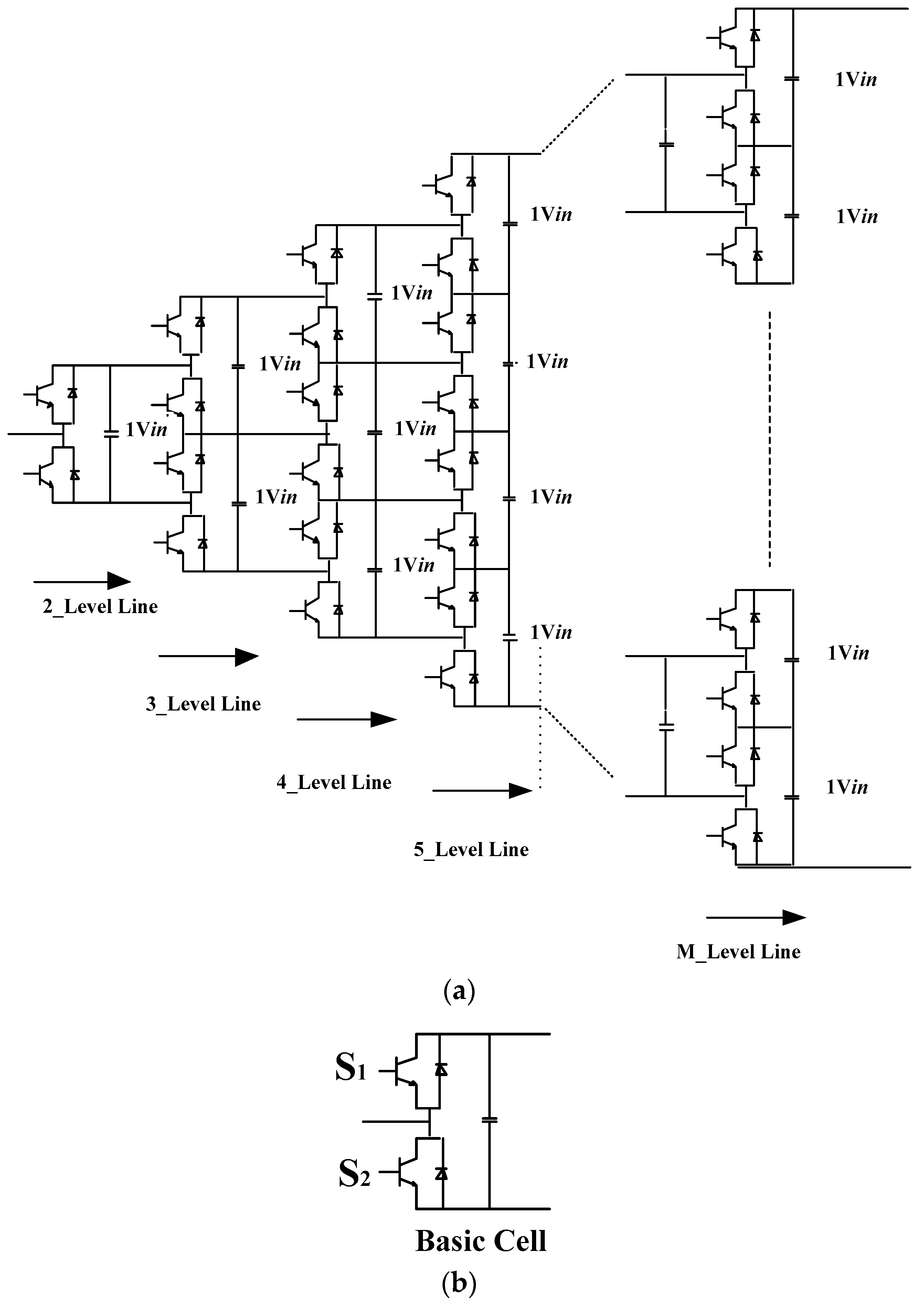
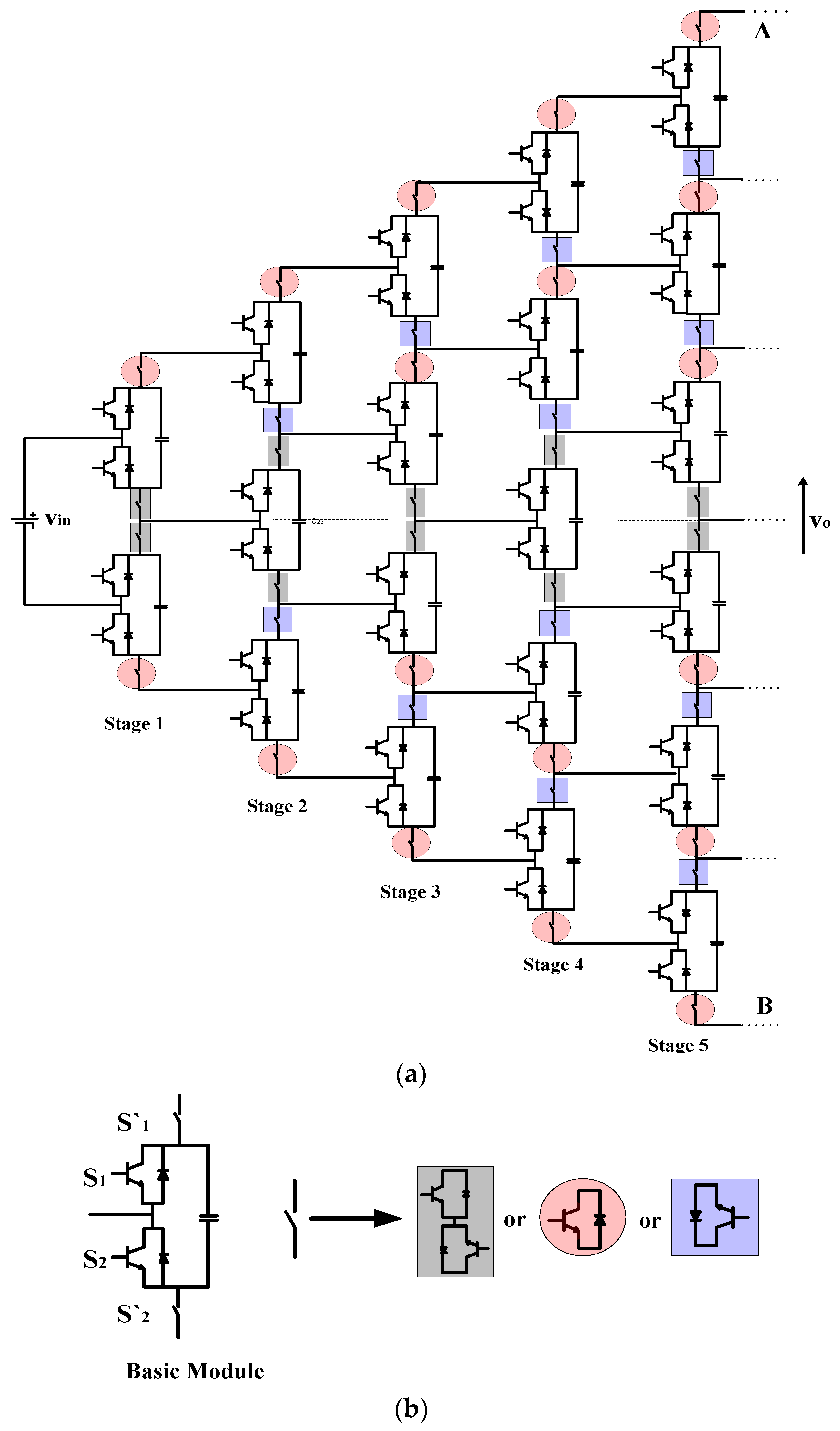
2. Proposed Topology

Figure 1a shows circuit topology of the multi-stage converter presented by F. Z. Peng et al. [24] where the capacitors of previous stages charge the capacitors of the next stages and then, the capacitors of the last stage generate multilevel AC voltage through a specific pulse pattern. Half-bridge building block modules (see Figure 1b) are used to connect the capacitors together. This module includes two two-quadrant switches (S1 and S2) which enable bidirectional current flow but can only block positive off-stage voltage. As the capacitors of the last stage are involved in output voltage generation and all capacitors are charged to Vin, the number of circuit components increases in order to achieve higher output voltages. This is because of the limitation of the building blocks to control the currents from different ports of the module. Charging capacitors to multiples of input voltage leads to decrement of circuit components. For this purpose, building blocks are required to control the current flow from three ports of the module. Two other switches (S′1 and S′2) are added to the module in order to control the current flow from different sides of the module. Figure 2a shows the configuration of the proposed converter where modified modules are used. Owing to the modified module (see Figure 2b), a number of capacitors are combined with power semiconductors to form a multi-stage switched-capacitor network. Special charging and discharging algorithms have to be considered to achieve multilevel output voltage through special arrangement of switches and capacitors. The main difference between the proposed topology and that shown in Figure 1 is the contribution of all the capacitors in multilevel voltage generation as well as charging the capacitors to multiples of Vin. As shown in Figure 2, S′1 and S′2 can be selected as unidirectional (two-quadrant switches that are shown in circle or square inclusion depending on the requirement for controlling current flow from one side) or bidirectional (four-quadrant switches that are shown in rectangular inclusion) switches.

3. Operating Principle of the Proposed Topology

Figure 3 shows a three-stage proposed converter where 9 modules and 42 switches (38 for SCMLI and 4 for H-bridge) are used. Note that the modules of the last stage can be simplified, and some of the switches can be eliminated. Smn is nth switch of mth module and CMi is the capacitor of ith module. A Switching state of (SM1, SM2, …, SM9) can be defined for this converter where SMi (i = 1, 2, …, 9) is the switching state for each module.

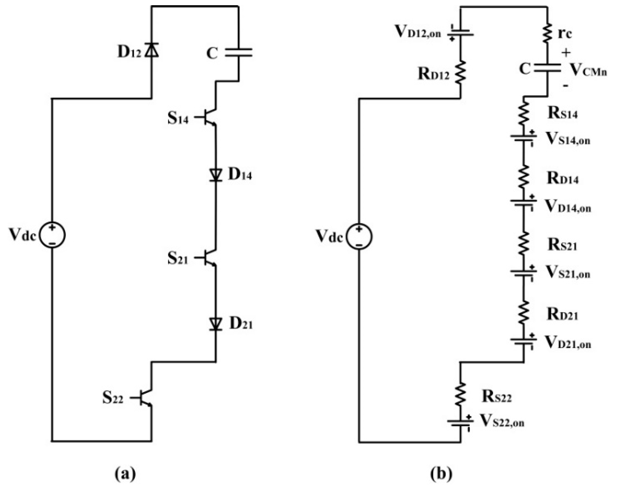
4. Asymmetrical Charging of the Capacitors

As mentioned, the main concept of this inverter is to charge the capacitors to multiples of the input voltage through switches. Figure 4 shows charging some states of different capacitors. As shown in Figure 4a, VCM1 reaches to Vin through the switches of modules 1 and 2. Voltage of CM3 reaches to 3Vin via CM1, CM2 and input DC source (see Figure 4b). CM6 and CM9 charges to 3Vin in parallel with CM3 and CM5 respectively (see Figure 4c). CM8 is charged to 14Vin via specified paths, which are shown in Figure 4d.
Some selected capacitor charging paths are indicated in Figure 4. According to this figure, by modeling each path, the equation of each capacitor voltage during charging can be achieved. The same scenario can be carried out for discharging paths to find equations of capacitors voltages during discharging intervals.
Figure 5 shows the model of charging circuit for CM1. In this model, the following non-idealities are considered for diodes, switches and capacitors:
  • VDij: Diode on-state voltage of ith module and jth diode
  • RDij: Diode on-state resistant of ith module and jth diode
  • rcn: ESR of nth capacitor
  • VSij: Switch on-state voltage of ith module and jth switch
  • RSij: RDij: Switch on-state resistant of ith module and jth switch
In the case of calculating capacitor voltage, there is a basic equation which compromised both power switches and diode voltage, which for the nth module during charge can be calculated as:
V C M n c h ( t ) = ( V i n M n ( k V S W , o n + m V D , o n ) ) ( 1 e t τ C M n )
There are different switches and diodes in each charging and discharging states and in the above equation, k and m are the number of switches and diodes in the charging paths respectively. CMn, V d c M n and τ C M n are capacitance value, input voltage and time constant of nth module. Time constant of CMn during charging can be calculated: (note that, on-resistance of the switches and diodes are considered as the same.)
τ C M n = ( k R s w + m R D + r c n ) · C M n
According to different modules in the proposed asymmetric multilevel inverter (see Figure 4) the input voltage of module 1 is V d c ( 3 V s w , o n + 3 V D , o n ) and its time constant is ( 3 R s w + 3 R D + r c ) · C M 1 . Therefore, V C M 1 can be shown as:
V C M 1 ( t ) = ( V d c ( 3 V S W , o n + 3 V D , o n ) ) ( 1 e t ( 3 R s w + 3 R D + r c ) · C M 1 )
The same procedure has to be carried out to calculate all of the capacitor voltages during charging. Table 1 shows different parameters for the calculation of all other capacitor voltages based on Equation (1), which also illustrates the number of switches and diodes in each path.

5. Multilevel Output Voltage Generation

Output voltage generation is carried out according to Table 2, i.e., the information provided about specific voltage generation for each module related to their possible switching states. To achieve a self-balanced system, charging and discharging states for the capacitors of each module should be available by switching pattern. To generate different levels, the ability of modules to keep the voltage within an acceptable range has to be analyzed. Therefore, Table 2 shows possible switching states for each module to generate mentioned output voltages. For each module, capacitor voltage is shown for the available switching states along with its charging or discharging mode. Note that “⨯” implies that mentioned switching state is not used at that specific module. Charging, discharging and no change mode of the module are shown with “▲”, “▼” and “–” respectively.
Having redundant states is an important issue in the generation of output voltage levels for multilevel inverters. According to Table 2, various alternatives are available for each module, which can be selected in order to balance the capacitors voltages. For instance, Module 1 is charged by switching state 5 and will be discharged by A, B and 9. States 0, 3 and C bypass CM1. State D also will charge this capacitor via input DC source. As shown in this table, whether the application of some switching states may lead to charging or discharging the capacitor depends on the switching state of the previous module.
With the same procedure as that used in the previous part, the voltage of each capacitor during discharging intervals can be calculated as:
V C M n D i s c h ( t ) = ( V C M n p ( t ) ( k V S W , o n + m V D , o n ) ) ( e t τ C M n )
where, V C M n D i s c h ( t ) is the discharge voltage of CMn and V C M n p ( t ) is the initial voltage of the capacitor before discharging. Other parameters (m and k) are the same as Table 1.
Choosing a proper switching pattern is the main challenge of this converter. Discharging the combination of capacitors across the load (to form different levels of output AC voltage) may lead to decrements in capacitor voltages. Therefore, to avoid capacitors voltage imbalance, switching states have to be used which are able to charge one or more capacitors during discharging time of other capacitors. This means that the charging time of all the capacitors should be distributed in the discharging intervals.
Table 3 shows the different switching states of the proposed converter to generate different levels. Note that proposed converter has hundreds of switching states, but only the switching states are mentioned in this table, which is crucial for capacitor voltage balancing. As shown in this table, at least one capacitor has the chance to be charged during the discharging of other capacitors (except 39Vin, 41Vin, 42Vin and 45Vin). Figure 6 shows the paths of charging and discharging for the four selected switching states.

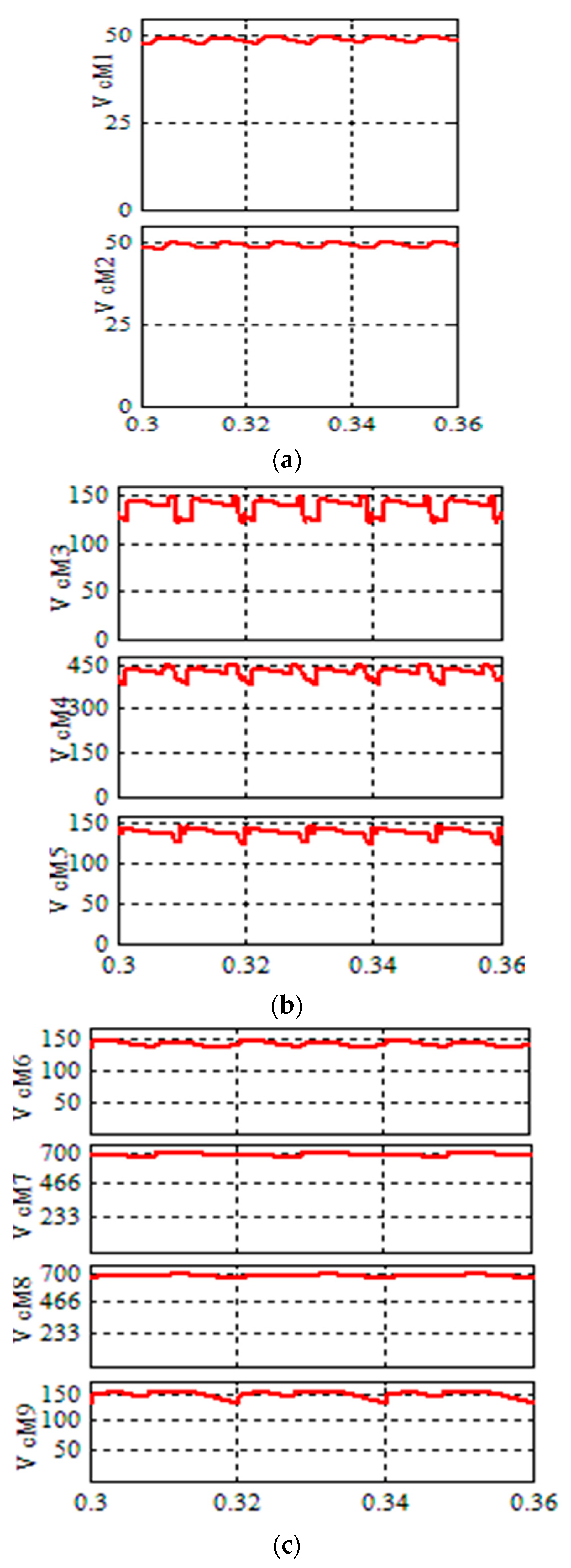
6. Capacitor Calculation for Self-Balancing Purpose

Generally, the maximum discharge amount of each capacitor CMn during the longest discharging period [t1, t2] can be calculated as [25]:
Q C M n = t 1 t 2 I o u t sin ( 2 π f s t ϕ ) d t
where fs is fundamental frequency, Iout is the amplitude of output current and ϕ is the phase difference between output current and voltage [19]. Considering QM1 and QM2 less than 10% maximum charge of CM1 and CM2 respectively, these capacitors can be achieved as:
C M 1 > Q c M 1 0.1 V i n
C M 2 > Q c M 2 0.1 V i n
As CM3 and CM5 are charged via DC source and series combination of CM1 and CM2, V C M 3 and V C M 5 are as follows:
V C M 3 = V i n + C M 1 · C M 2 C M 1 + C M 2 C M 1 · C M 2 C M 1 + C M 2 + C M 3 × ( V C M 1 + V C M 2 )
V C M 5 = V i n + C M 1 · C M 2 C M 1 + C M 2 C M 1 · C M 2 C M 1 + C M 2 + C M 5 × ( V C M 1 + V C M 2 )
Therefore, CM3 and CM5 are obtained as:
C M 3 = [ ( C M 1 · C M 2 C M 1 + C M 2 ) × ( V C M 1 + V C M 2 ) ] + V i n V C M 3 ( C M 1 · C M 2 C M 1 + C M 2 )
C M 5 = [ ( C M 1 · C M 2 C M 1 + C M 2 ) × ( V C M 1 + V C M 2 ) ] + V i n V C M 5 ( C M 1 · C M 2 C M 1 + C M 2 )
With the same procedure, other capacitors and their voltages can be calculated as:
V C M 4 = V i n + ( ( 1 C M 1 + 1 C M 2 + 1 C M 3 + 1 C M 5 ) ( 1 C M 1 + 1 C M 2 + 1 C M 3 + 1 C M 5 ) + C M 4 ) × ( V C M 1 + V C M 2 + V C M 3 + V C M 5 )
V C M 6 = C M 3 C M 3 + C M 6 × ( V C M 3 )
C M 6 = ( C M 3 × V C M 3 ) + V i n V C M 6 C M 3
V C M 9 = C M 5 C M 5 + C M 9 × ( V C M 5 )
C M 9 = ( C M 5 × V C M 5 ) + V i n V C M 9 C M 5
V C M 7 = V i n + ( ( 1 C M 1 + 1 C M 3 + 1 C M 4 ) ( 1 C M 1 + 1 C M 3 + 1 C M 4 ) + C M 7 ) × ( V C M 1 + V C M 3 + V C M 4 )

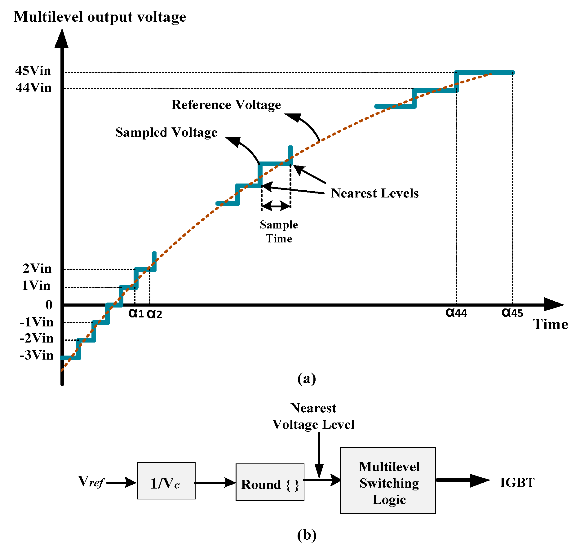
7. Modulation Strategy and Switching States Selection

This is an important factor in capacitor voltage balancing due to the definition of charging and discharging intervals which are required for voltage calculations for capacitors. In this study, a predetermined offline PWM strategy was considered to define the switching angles (the angles in which the levels change). Figure 7a shows a sampled staircase multilevel voltage waveform and a reference voltage in a Nearest Level Control (NLC) modulation technique. Figure 7b shows the schematic block diagram of this strategy. The nearest output voltage level Vn can be determined with [26]:
V n = 1 V c r o u n d ( V r e f )
After determination of each voltage level and its time duration, a precise switching selection has to be carried out according to Table 3. The selection of one state for each level defines the charging or discharging states of each capacitor, which is an important task to keep the voltages within an acceptable range.

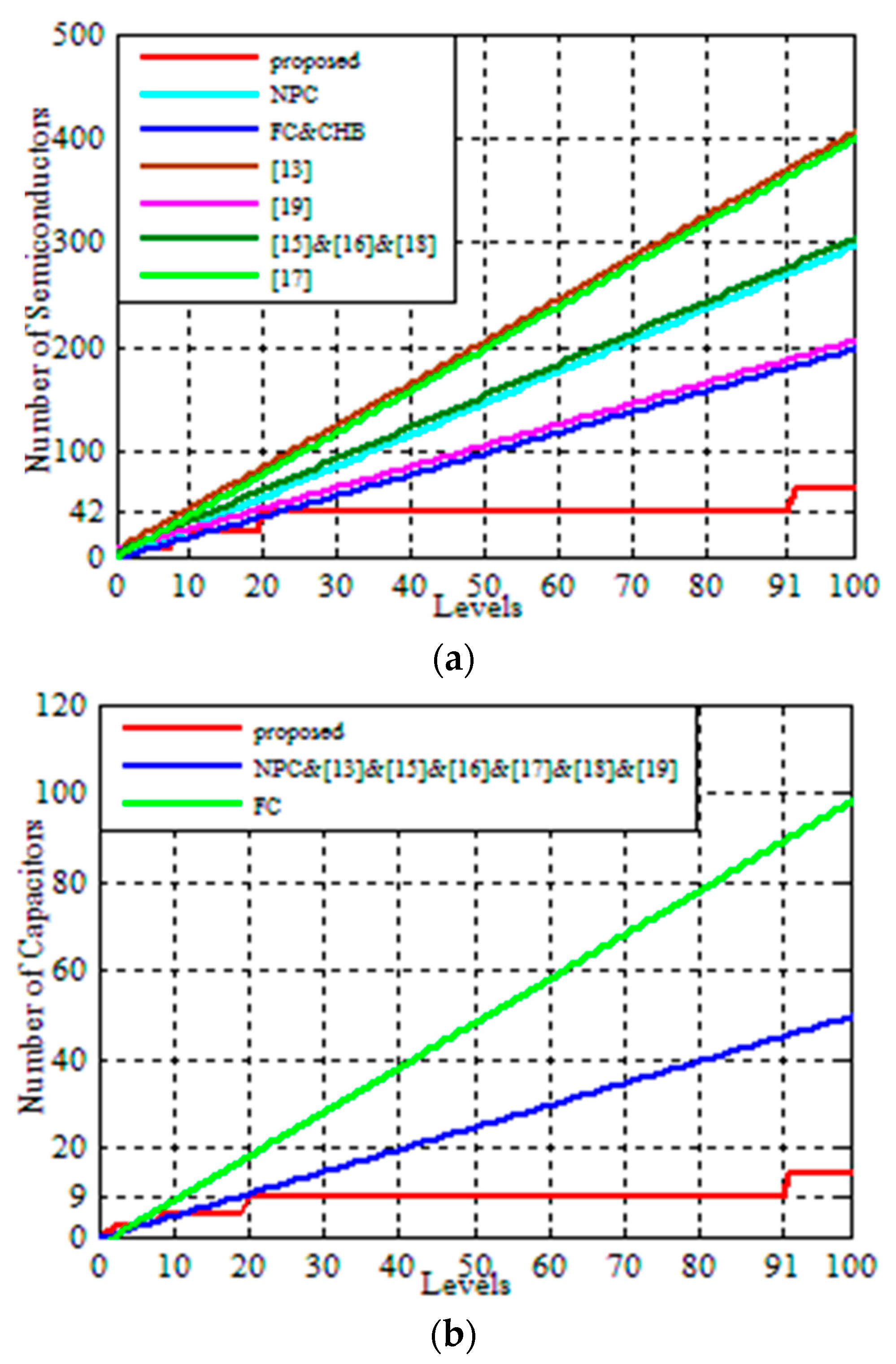
8. Comparison with Other Topologies

A comparative study is carried with other famous topologies which are presented at [13,15,16,17,18,19]. Table 4 shows the number of switching devices (Active switches, series diode), drivers for the switches and capacitors versus number of levels (NL) and number of stages for the proposed inverter (nstage). Note that, as shown in Figure 8, the relation between the number of stages and the number of levels in the proposed converter is:
n s t a g e = { 1    0 N L 19 2    19 N L 91 3    91 N L 253
Figure 8 presents the number of capacitors and semiconductors (active switches + series diodes) for 0 to 100 levels output. This comparison shows that the proposed converter provides better performance in terms of the number of components. As the converter is for low voltage input voltage sources, multiples of this low voltage amount are still within the acceptable standard range of components.

9. The Simulation Results

A MATLAB simulation is conducted to achieve a 91-level output voltage with a maximum of 45 times of input DC voltage. The parameters given in Table 5 are used for the analysis.
Figure 9a,b show the output voltage and current at 50 Hz for two types of resistive and resistive-inductive loads. As shown in these figures, a high level staircase output voltage is achieved. Discharging currents of the last stage capacitors are shown in Figure 9c,d. The converter and its control strategy are able to balance capacitor voltages within acceptable ranges with considered tolerances (see Figure 10a–c). FFT analysis of the output voltage is shown in Figure 11, which indicates good performance of the proposed topology because of its low harmonic distortion.

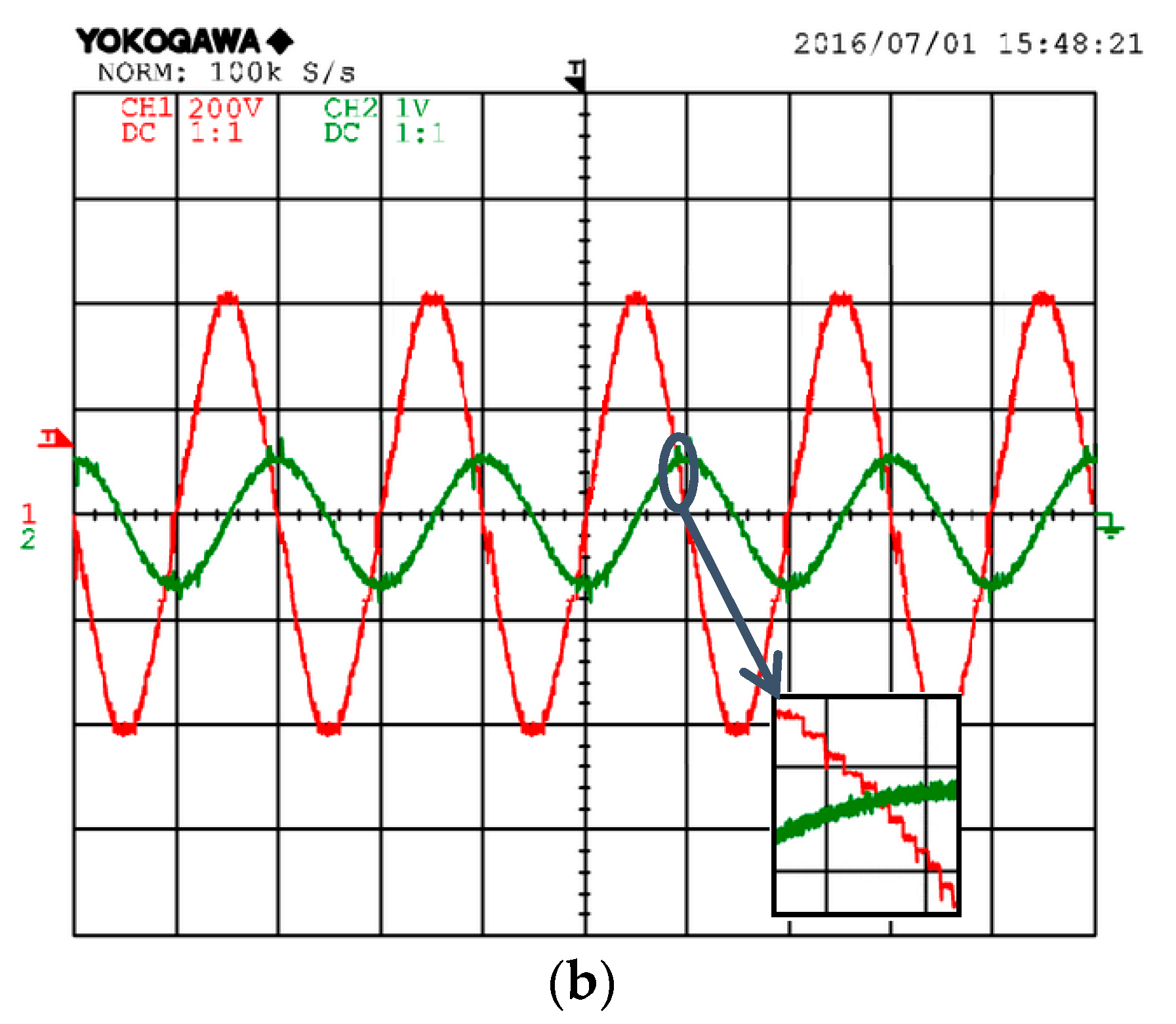
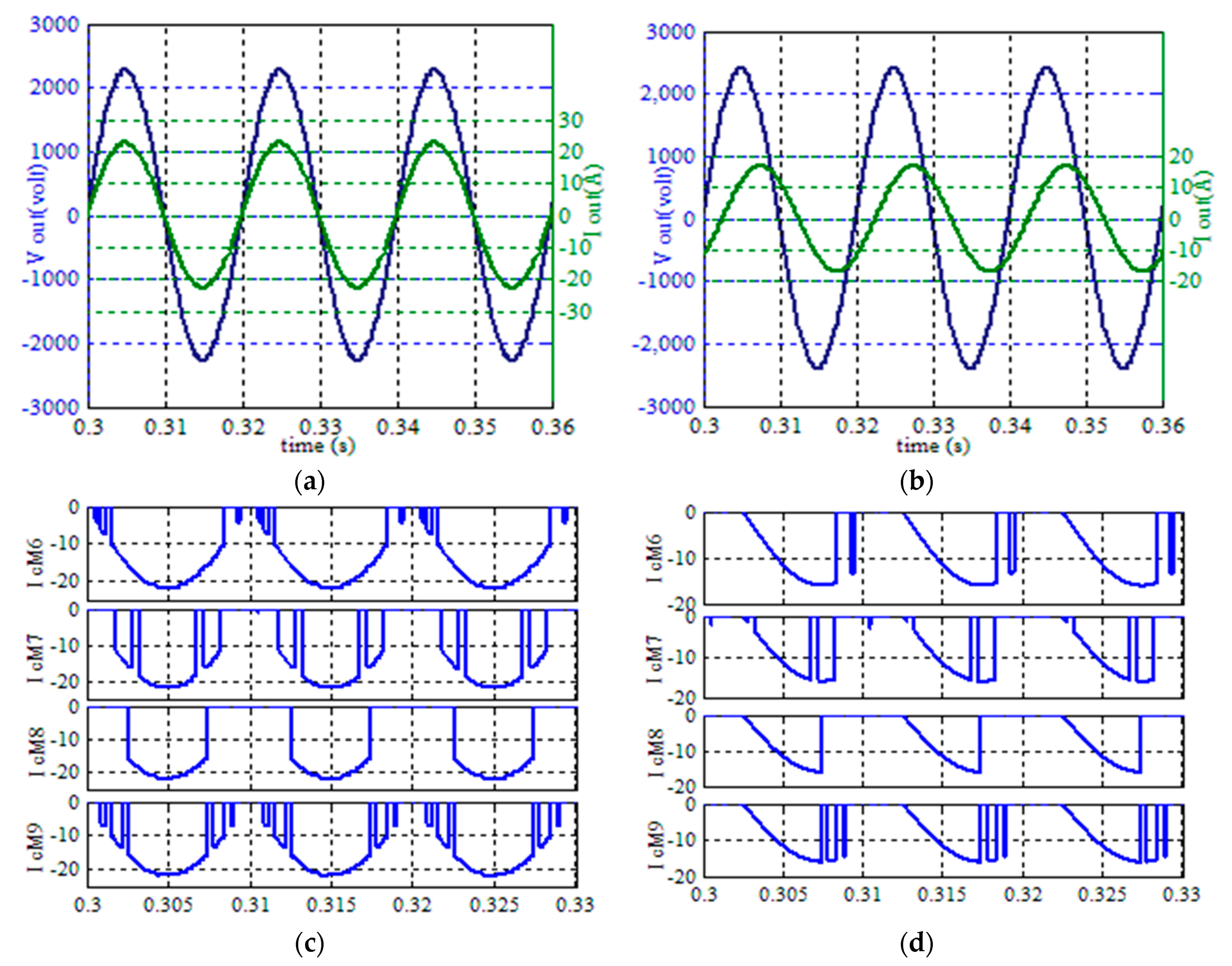
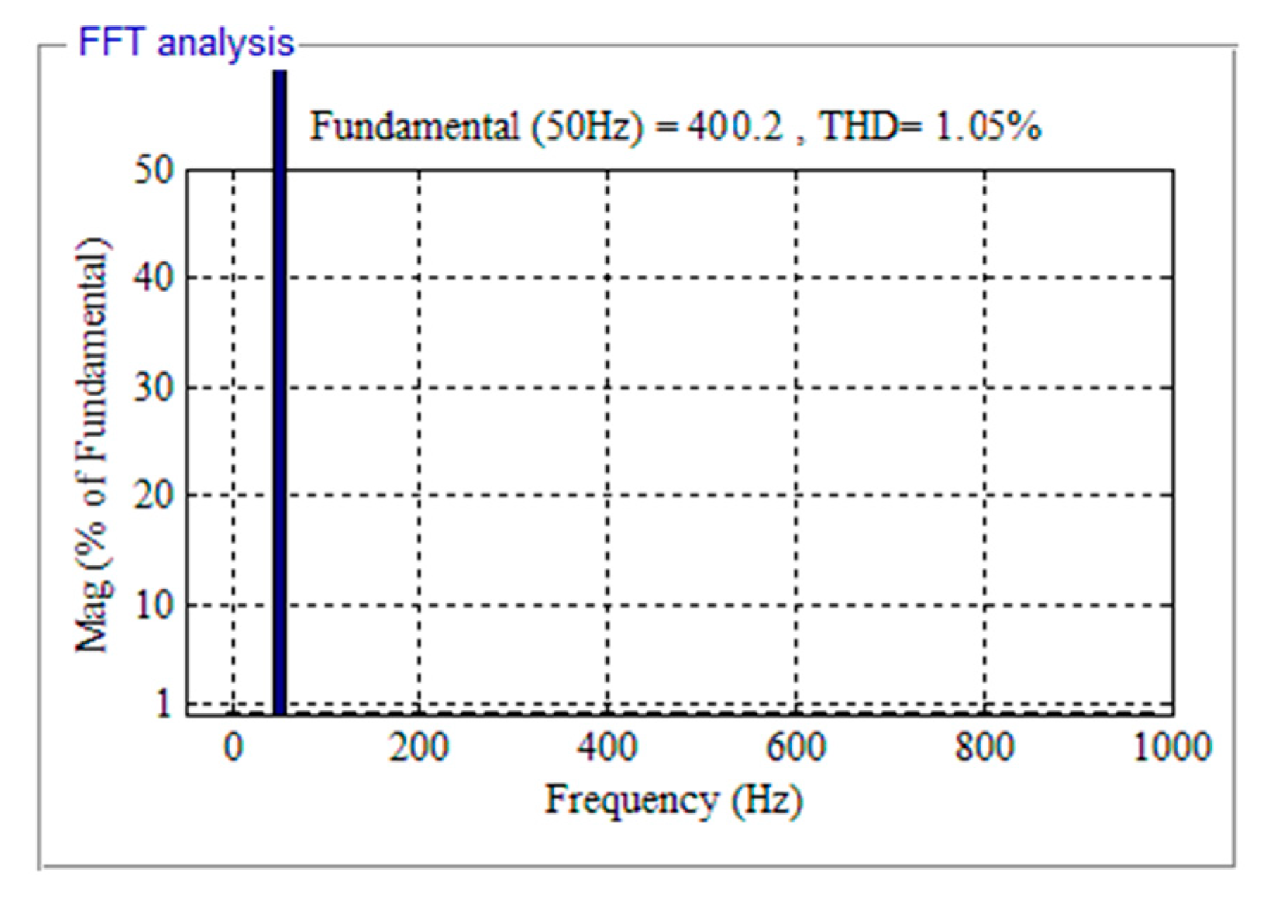
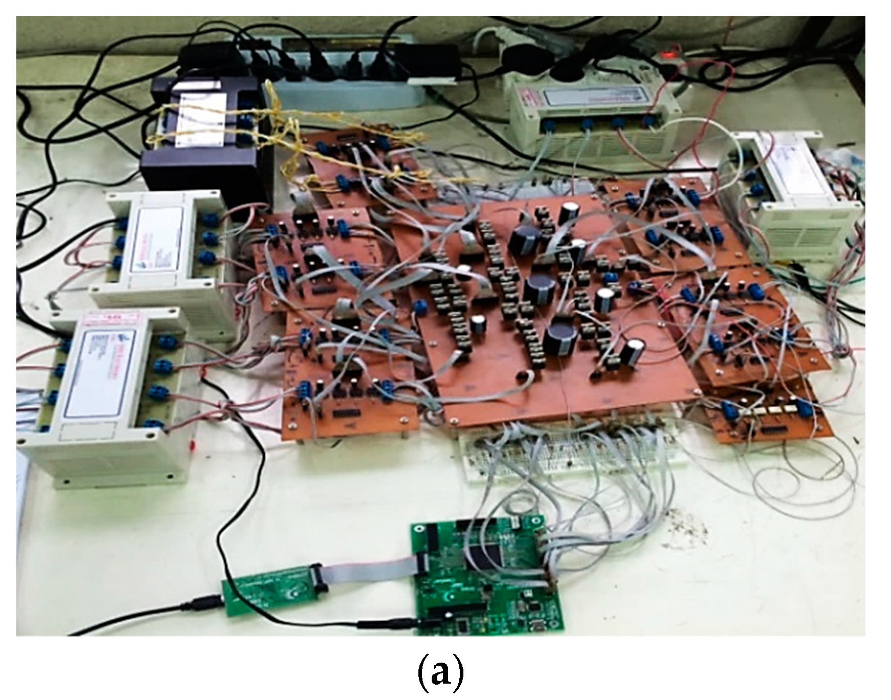
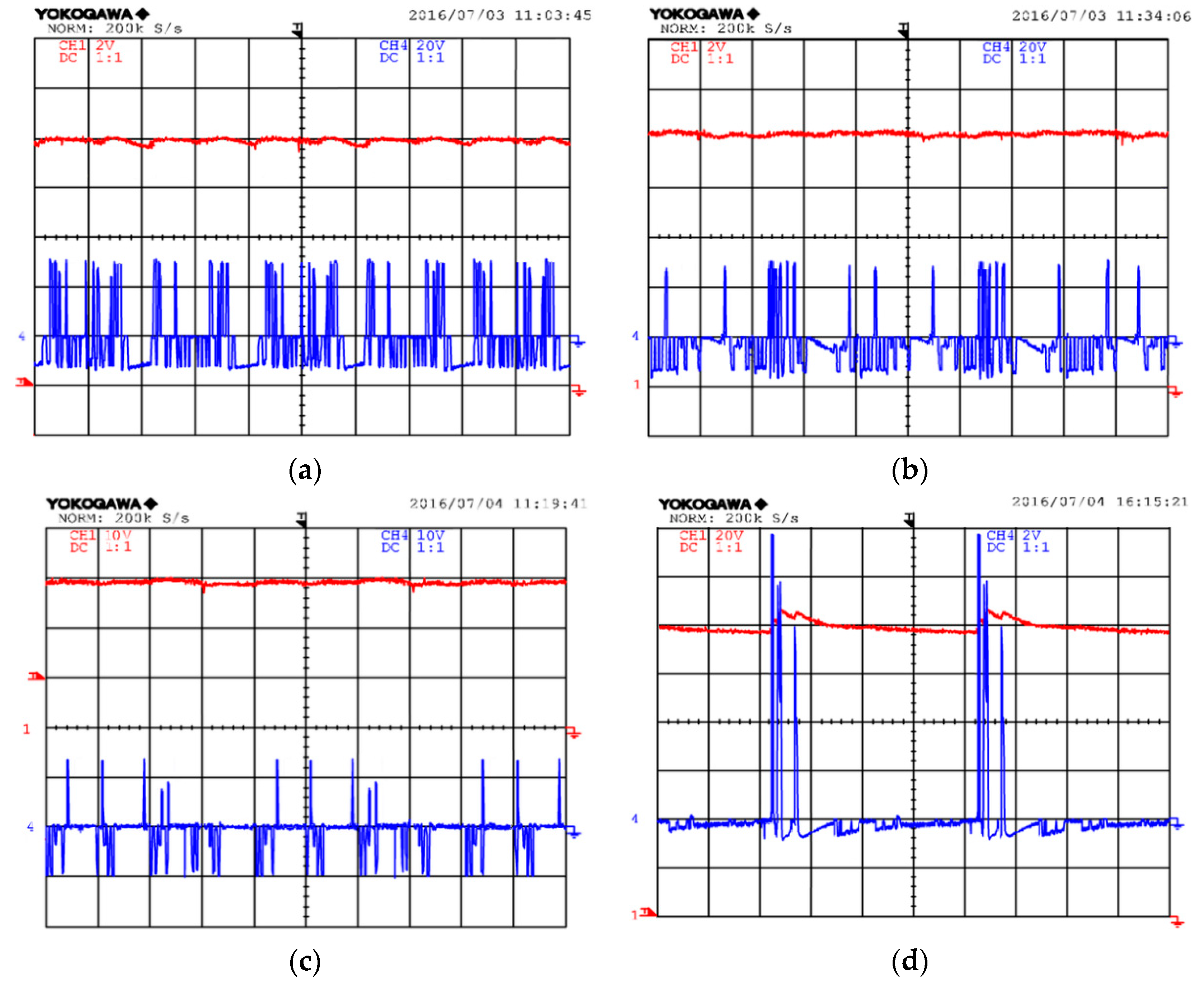
10. Experimental Results

To validate our simulation and analysis, an experimental test setup was built with an input voltage of 10 volts, as shown in Figure 12a; other components are shown at Table 6. Figure 12b shows the output voltage and current for a pure inductive load, which confirms the application of the proposed structure and its mentioned control strategy under different operating conditions.
Figure 13a–d shows the voltages and currents of selected capacitors (CM1, CM2, CM3, CM7) over a 2.5 ms period. It is clear that the number of charges and discharges for the capacitors in the first stage is much higher than that in last stages.

11. Conclusions

An asymmetrical step-up multilevel inverter is presented in this paper with a single DC source. Bidirectional modules are designed in order to create different paths for the capacitors to be charged or discharged, based on a predetermined pattern. A comprehensive mathematical analysis is conducted to achieve capacitance values and the voltage of each capacitor during the different states. Investigation of a three-stage proposed converter showed that 45 levels can be achieved using different switching states. The application of a full bridge single phase inverter at the end of the proposed converter gives 91 voltage levels (45 positive, 45 negative and one zero level). According to a detailed comparison with other classical and state-of-the-art topologies, the number of different components was reduced to a great extent. A comprehensive simulation study and experimental results are presented to verify the analysis.

Author Contributions

All authors contributed equally to this work and all authors have read and approved the final manuscript.

Funding

This research received no external funding.

Conflicts of Interest

The authors declare no conflict of interest.

References

  1. Mohan, N.; Undeland, T.M.; Robbins, W.P. Power Electronics: Converters, Applications and Design, 3rd ed.; John Wiley & Sons: Hoboken, NJ, USA, 2003. [Google Scholar]
  2. Nabae, N.; Takahashi, I.; Akagi, H. A new neutral point clamped PWM inverter. IEEE Trans. Ind. Appl. 1981, 17, 518–523. [Google Scholar] [CrossRef]
  3. Zare, F. Power Electronics Education Electronic-Book, 1st ed.; School of Engineering Systems, Queensland University of Technology: Brisbane, Australia, 2008. [Google Scholar]
  4. Khenar, M.; Taghvaie, A.; Adabi, J.; Rezanejad, M. Multi-level inverter with combined T-type and cross-connected modules. IET Power Electron. 2018, 11, 1407–1415. [Google Scholar] [CrossRef]
  5. Vahedi, H.; Labbe, P.A.; Haddad, K.A. Sensor-Less Five-Level Packed U-Cell (PUC5) Inverter Operating in Stand-Alone and Grid-Connected Modes. IEEE Trans. Ind. Inform. 2016, 12, 361–370. [Google Scholar] [CrossRef]
  6. Taghvaie, A.; Adabi, J.; Rezanejad, M. A Multilevel Inverter Structure Based on a Combination of Switched-Capacitors and DC Sources. IEEE Trans. Ind. Inform. 2017, 13, 2162–2171. [Google Scholar] [CrossRef]
  7. Taghvaie, A.; Adabi, J.; Rezanejad, M. Circuit Topology and Operation of a Step-Up Multilevel Inverter with a Single DC Source. IEEE Trans. Ind. Electron. 2016, 63, 6643–6652. [Google Scholar] [CrossRef]
  8. Samsami, H.; Taheri, A.; Samanbakhsh, R. New bidirectional Multilevel inverter topology with staircase cascading for symmetric and asymmetric structures. IET Power Electron. 2017, 10, 1315–1323. [Google Scholar] [CrossRef]
  9. Ali, J.S.M.; Alishah, R.S.; Sandeep, N.; Hosseini, S.H.; Babaei, E.; Vijayakumar, K.; Yaragatti, U.R. A new generalized multilevel converter topology based on cascaded connection of basic units. IEEE J. Emerg. Sel. Top. 2018. [Google Scholar] [CrossRef]
  10. Pereda, J.; Dixon, J. High-frequency link: A solution for using only one DC source in asymmetric cascaded multilevel invrter. IEEE Trans. Ind. Electron. 2011, 58, 3884–3893. [Google Scholar] [CrossRef]
  11. Vijeh, M.; Rezanejad, M.; Samadaei, E.; Bertilson, K. A general review on multilevel inverters based on main submodule: Structural point of view. IEEE Trans. Power Electron. 2019. [Google Scholar] [CrossRef]
  12. Gautam, S.P.; Sahu, L.K.; Gupta, S. Reduction in number of devices for symmetrical and asymmetrical multilevel inverters. IET Power Electron. 2016, 9, 698–709. [Google Scholar] [CrossRef]
  13. Chattopadhyay, S.K.; Chakraborty, C. A New Multilevel Inverter Topology with Self-Balancing Level Doubling Network. IEEE Trans. Ind. Electron. 2014, 61, 4622–4631. [Google Scholar] [CrossRef]
  14. Tseng, K.C.; Huang, C.C.; Shih, W.Y. A High Step-Up Converter with a Voltage Multiplier Module for a Photovoltaic System. IEEE Trans. Power Electron. 2013, 28, 3047–3057. [Google Scholar] [CrossRef]
  15. Du, Z.; Ozpineci, B.; Tolbert, L.M.; Chiasson, J.N. DC-AC cascaded H-bridge multilevel boost inverter with no inductors for electric/hybrid electric vehicle applications. IEEE Trans. Ind. Appl. 2009, 45, 963–970. [Google Scholar] [CrossRef]
  16. Lee, S.S.; Chu, B.; Rumzi, N.; Idris, N.; Goh, H.H.; Heng, Y.E. Switched-Battery Boost-Multilevel Inverter with GA Optimized SHEPWM for Standalone Application. IEEE Trans. Ind. Electron. 2016, 63, 2133–2142. [Google Scholar] [CrossRef]
  17. Mak, O.C.; Ioinovici, A. Switched-capacitor inverter with high power density and enhanced regulation capability. IEEE Trans. Circuits Syst. I Fundam. Theory Appl. 1998, 45, 336–347. [Google Scholar]
  18. Liu, Y.; Luo, F.L. Multilevel inverter with the ability of self-voltage balancing. IEE Proc. Electr. Power Appl. 2006, 153, 105–115. [Google Scholar] [CrossRef]
  19. Hinago, Y.; Koizumi, H. A Switched-Capacitor Inverter Using Series/Parallel Conversion with Inductive Load. IEEE Trans. Ind. Electron. 2012, 59, 878–887. [Google Scholar] [CrossRef]
  20. Babaei, E.; Gowgani, S.S. Hybrid multilevel inverter using switched-capacitor units. IEEE Trans. Ind. Electron. 2014, 61, 4614–4621. [Google Scholar] [CrossRef]
  21. Barzegarkhoo, R.; Kojabadi1, H.M.; Zamiry, E.; Vosooghi, N.; Chang, L. Generalized Structure for a Single Phase Switched-Capacitor Multilevel Inverter Using a New Multiple DC Link Producer with Reduced Number of Switches. IEEE Trans. Power Electron. 2016, 31, 5604–5617. [Google Scholar] [CrossRef]
  22. Ye, Y.; Cheng, K.W.E.; Liu, J.; Ding, K. A Step-Up Switched-Capacitor Multilevel Inverter with Self Voltage Balancing. IEEE Trans. Ind. Electron. 2014, 61, 6672–6680. [Google Scholar] [CrossRef]
  23. Ebrahimi, J.; Babaei, E.; Gharehpetian, G.B. A New Multilevel Converter Topology with Reduced Number of Power Electronic Components. IEEE Trans. Ind. Electron. 2012, 59, 655–667. [Google Scholar] [CrossRef]
  24. Peng, F.Z. A Generalized Multilevel Inverter Topology with Self Voltage Balancing. IEEE Trans. Ind. Appl. 2001, 37, 611–618. [Google Scholar] [CrossRef]
  25. Taghvaie, A.; Adabi, J.; Rezanejad, M. A Self-Balanced Step-up Multilevel Inverter based on Switched-Capacitors Structure. IEEE Trans. Power Electron. 2018, 33, 199–209. [Google Scholar] [CrossRef]
  26. Meshram, P.M.; Borghate, V.B. A Simplified Nearest Level Control (NLC) Voltage Balancing Method for Modular Multilevel Converter (MMC). IEEE Trans. Power Electron. 2015, 30, 450–462. [Google Scholar] [CrossRef]
Figure 1. (a) Presented topology of [20] (b) its basic cell.
Sustainability 11 03453 g001
Figure 2. Proposed topology (a) Switched-capacitor structure, (b) Its building block modules.
Sustainability 11 03453 g002
Figure 3. Diagram of a three-stage proposed inverter.
Sustainability 11 03453 g003
Figure 4. Charging states of different capacitors.
Sustainability 11 03453 g004
Figure 5. Charging path of CM1 (a) Real circuit, (b) its non-idealises model.
Sustainability 11 03453 g005
Figure 6. charging and discharging paths for selected switching states.
Sustainability 11 03453 g006
Figure 7. Nearest Level Control (a) Waveform synthesis, (b) Block diagram.
Sustainability 11 03453 g007
Figure 8. Comparison between proposed topology and others (a) number of semiconductors (active switches+ series diodes), (b) number of capacitors.
Sustainability 11 03453 g008
Figure 9. Simulation results (a) Output voltage and currents R load, (b) Output voltage and currents R-L load, (c) Discharging current of the last stage capacitors with R-load, (d) Discharging current of the last stage capacitors with R-L load.
Sustainability 11 03453 g009
Figure 10. Capacitor’s voltage in (a) first stage, (b) second stage, (c) third stage.
Sustainability 11 03453 g010
Figure 11. FFT analysis of output voltage.
Sustainability 11 03453 g011
Figure 12. Experimental results (a) Test set up (volt/div = 200 volts), (b) Output voltage and current in pure inductive load (Ampere/div = 1 amps) (time/div = 2500 μs).
Sustainability 11 03453 g012aSustainability 11 03453 g012b
Figure 13. Voltage and current of capacitors (all channels time/div = 2500 μs) (a) CM1 (volt/div = 2 volts, Ampere/div = 20 amps), (b) CM2 (volt/div = 2 volts, Ampere/div = 20 amps), (c) CM3 (volt/div = 10 volts, Ampere/div = 10 amps), (d) CM7 (volt/div = 20 volts, Ampere/div = 2 amps).
Sustainability 11 03453 g013
Table 1. Different parameters for different capacitors.
n V i n M n km
2 V d c 33
3 V d c + V C M 1 ( t ) + V C M 2 ( t ) 66
4 V d c + V C M 1 ( t ) + V C M 2 ( t ) + V C M 3 ( t ) + V C M 5 ( t ) 128
5 V d c + V C M 1 ( t ) + V C M 2 ( t ) 66
6 V C M 3 ( t ) 33
7 V d c + V C M 1 ( t ) + V C M 3 ( t ) + V C M 4 ( t ) 106
8 V d c + V C M 2 ( t ) + V C M 4 ( t ) + V C M 5 ( t ) 106
9 V C M 5 ( t ) 33
Table 2. possible switching states for each module and voltage state of each capacitor (Charge: ▲, Discharge: ▼, No Change: -).
VCM1VCM2VCM3VCM4VCM5VCM6VCM7VCM8VCM9
0(0000)0 (-)0 (-)0 (-)0 (-)0 (-)0 (-)0 (-)0 (-)3Vin (▼)
2(0010)3Vin (▼)14Vin(▼,▲)14Vin (▼,▲)
3 (0011)0 (-)0 (-)0 (-)0 (-)0 (-)
4(0100)3Vin (▼)14Vin (▼)14Vin (▼)0 (-, ▲)
5(0101)−1Vin (▲)1Vin (▼)−3Vin (▲)9Vin (▼)
−9Vin (▼)
3Vin (▼)
6(0110)0 (-)0 (-)0 (-)_
8(1000)0 (-)0 (-)0 (-)3Vin(▼)
9(1001)1Vin(▼)1Vin(▼)3Vin(▼)9Vin (▲▼)
−9Vin(▼)
3Vin(▼)
A(1010)1Vin(▼)−1Vin(▲)3Vin(▼)9Vin (▼)
−9Vin (▼)
−3Vin (▲)3Vin (▲)14Vin (▼)14Vin (▼)
B(1011)1Vin (▼)1Vin (▲)3Vin (▼)3Vin (▲)
C(1100)0 (-)0 (-)0 (-)0 (-)
D(1101)1Vin (▲)1Vin (▼)3Vin (▲)3Vin (▼)
Table 3. Different switching states of proposed converter.
LevelSwitching States (CM1, CM2, CM3, CM4, CM5, CM6, CM7, CM8, CM9)
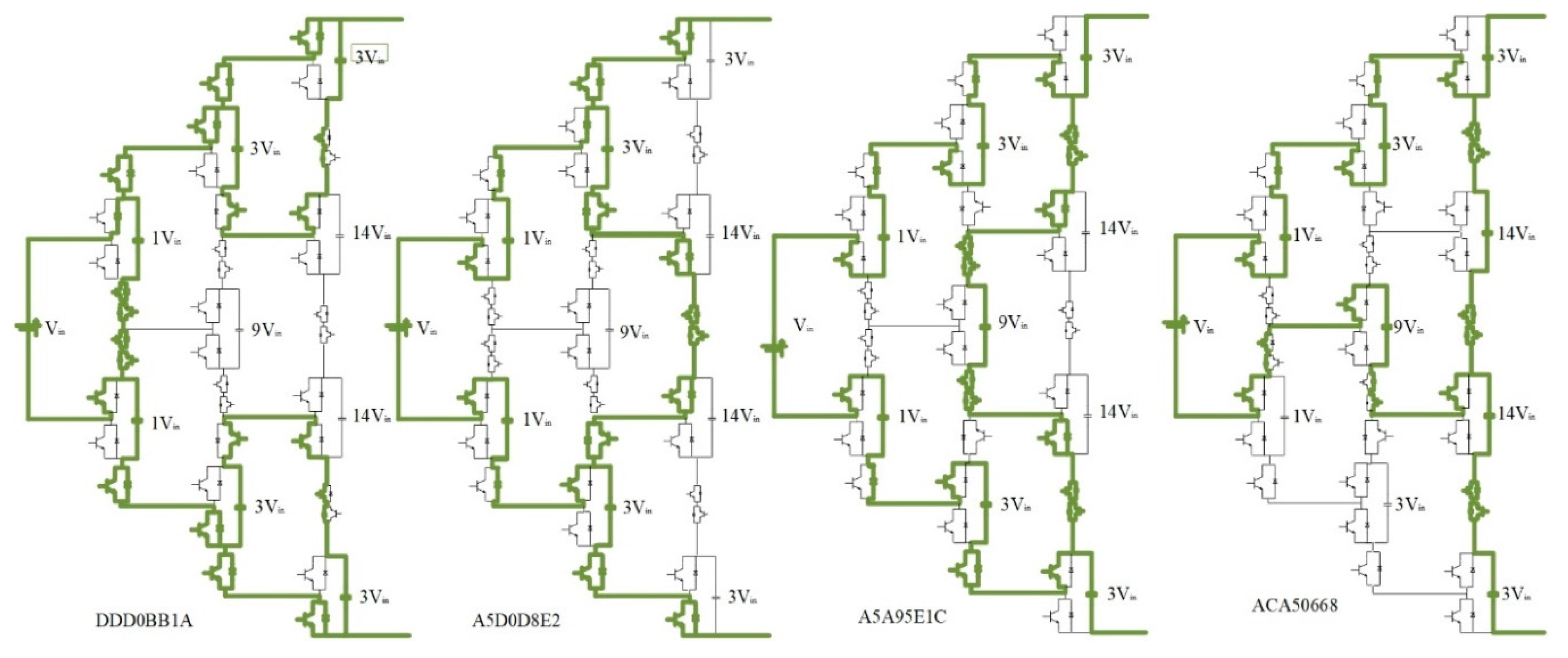
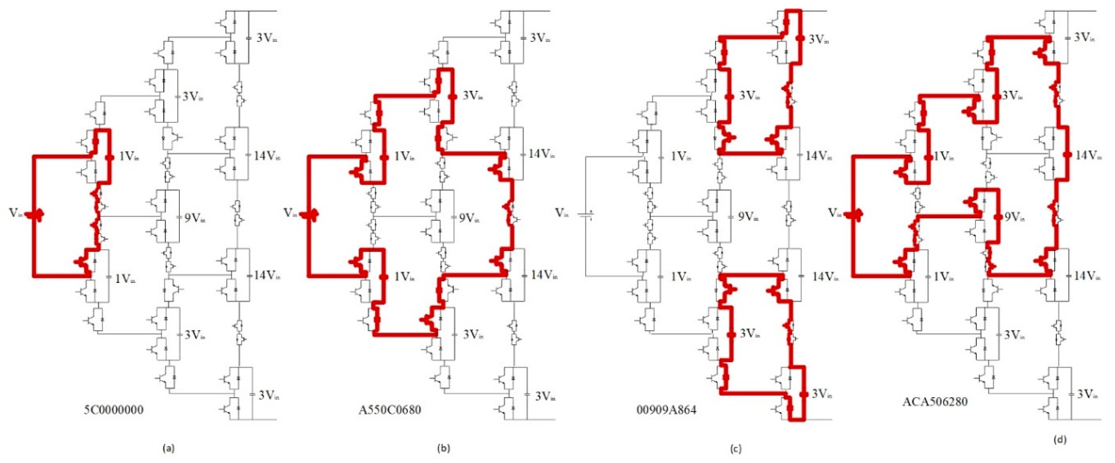
0VIN5C0000000(↑− − − − − − − −) 3A0000000(−↑− − − − − − −) A550C0680(↓↓↑− − − − − −) A530A0680(↓↓− −↑− − − −) A5A956868 (↓↓↓↑↓− − − −) 00909A864(− −↓−↓↑− −↑) ACA506280(↓−↓↓− −↑− −) 350A50628(−↓−↓↓− −↑ −)
1VINC3D0BA864(− −↓−↓↑− −↑)
2VINBBD0BA864(↓↑↓−↓↑− −↑) DDD0BA864(↑↓↓−↓↑− −↑)
3VINA5D0BA864(↓↓↓−↓↑− −↑)
4VIN5D9CBA864(↑↓↓−↓↑− −↑) 3B9CBA864(↓↑↓−↓↑− −↑) BAD39A864(↓↑↓−↓↑− −↑) DCD39A864(↑↓↓−↓↑− −↑)
5VIN BBB0BA864(↓↑↓−↓↑− −↑) DDB0BA864(↑↓↓−↓↑− −↑) BBD0DA864(↓↑↓−↓↑− −↑ DDD0DA864(↑↓↓−↓↑− −↑)
6VINA5D0D8684(↓↓↑−↓− − − −) A5B0B8684(↓↓↓−↑− − − −) 5C9098684(↑−↓−↓− − − −) 3A9098684(−↑↓−↓− − − −) A5B0BA864(↓↓↓−↓↑− −↑) A5D0DA864(↓↓↓−↓↑− −↑)
7VINBAD39A804(↓↑↓−↓↑− −↑) DCD39A804(↑↓↓−↓↑− −↑) 5D9CDA864(↑↓↓−↓↑− −↑) 3B9CDA864(↓↑↓−↓↑− −↑)
8VINDDB0DA864(↑↓↓−↓↑− −↑) BBB0DA864(↓↑↓−↓↑− −↑)
9VINA5B0DA864(↓↓↓−↓↑− −↑) A5B0B8688(↓↓↓−↑− − −↓) A5D0D8688(↓↓↑−↓− − −↓) 5C9094684(↑−↓−↓↓− − −)3A9094684(−↑↓−↓↓− − −)
10VINBAB39A808(↓↑↓−↓↑− −) DCB39A808(↑↓↓−↓↑− −↓) 5D9CD4064(↑↓↓−↓↓− −↑) 3B9CD4064(↓↑↓−↓↓− −↑)
11VINDDA0D4064(↑↓↓−↓↓− −↑) BBA0D4064(↓↑↓−↓↓− −↑) DDB05A808(↑↓↓−↓↑− −↓) BBB05A808(↓↑↓−↓↑− −↓)
12VIN5C9094688(↑−↓−↓↓− −↓) 3A9094688(−↑↓−↓↓− −↓) A5D0D4688(↓↓↑−↓↓− −↓) A5B0B4688(↓↓↓−↑↓− −↓) A5B05A808(↓↓↓−↓↑− −↓) A5A0D4064(↓↓↓−↓↓− −↑)
13VIN5D9ABA864(↑↓↓↓↓↑− −↑) 3B9ABAA864(↓↑↓↓↓↑− −↑) BAD59A864(↓↑↓↓↓↑− −↑) DCD59A864(↑↓↓↓↓↑− −↑)
14VIN359ABA864(−↓↓↓↓↑− −↑) ACD59A864(↓−↓↓↓↑− −↑)
15VINA5A956868(↓↓↓↑↓↓− −↓) 5C999A864(↑−↓↓↓↑− −↑) 3A999A864(−↑↓↓↓↑− −↑)
16VIN5D9ADA864(↑↓↓↓↓↑− −↑) BAB59A864(↓↑↓↓↓↑− −↑)
17VIN359ADA864(−↓↓↓↓↑− −↑)
18VIN5C999A808(↑−↓↓↓↑− −↓) 5C9994064(↑−↓↓↓↓− −↑) 3A999A808(−↑↓↓↓↑− −↓) 3A9994064(−↑↓↓↓↓− −↑)
19VINDD30B2464(↑↓− −↓↓↓−↑) DDD0CA8A0(↑↓↓− −↑−↓↓) BB30B2464(↓↑− −↓↓↓−↑) BBD0CA8A0(↓↑↓− −↑−↓↓)
20VINACA596284(↓−↓↓↓↓↑− −) A550D2684(↓↓↑−↓↓↓− −) 359A58628(−↓↓↓↓− −↑↓) A530B2684(↓↓− −↑↓↓− −) 5C9008620(↑−↓− − − −↓↓) 3A9008620(−↑↓− − − −↓↓)
21VIN5C9994008(↑−↓↓↓↓− −↓) 3A9994008(−↑↓↓↓↓− −↓)
22VINDD30D2464(↑↓− −↓↓↓−↑) BB30D2464(↓↑− −↓↓↓−↑) DDD0CA8A0(↑↓↓− −↑−↓↓) BBD0CA8A0(↓↑↓− −↑−↓↓)
23VINACA596288(↓−↓↓↓↓↑−↓) 359A54628(−↓↓↓↓↓−↑↓) A5D0C46A0(↓↓↑− −↓−↓↓) A550D2688(↓↓↑−↓↓↓−↓) A5B0A46A0(↓↓↓−↑↓−↓↓) A530B2688(↓↓− −↑↓↓−↓)
24VIN5D0C52408(↑↓− −↓↓↓−↓) 3B0C52408(↓↑− −↓↓↓−↓) BAA3040A0(↓↑↓− −↓−↓↓) DCA3040A0(↑↓↓− −↓−↓↓)
25VINDD3052408(↑↓− −↓↓↓−↓) BB3052408(↓↑− −↓↓↓−↓) DDA0C40A0(↑↓↓− −↓−↓↓) BBA0C40A0(↓↑↓− −↓−↓↓)
26VIN5C9094A88(↑−↓−↓↓↓−↓) 3A9094A88(−↑↓−↓↓↓−↓) 5C9094648(↑−↓−↓↓−↓↓) 3A9094648(−↑↓−↓↓−↓↓)
27VIN5D0AB2464(↑↓−↓↓↓↓−↑) BAD50A8A0(↓↑↓↓−↑−↓↓)
28VINACD50A8A0(↓−↓↓−↑−↓↓) 350AB2464(−↓−↓↓↓↓−↑)
29VIN5C0992404(↑− −↓↓↓↓− −) 3A0992404(−↑−↓↓↓↓− −) 5C99080A0(↑−↓↓− − −↓↓) 3A99080A0(−↑↓↓− − −↓↓)
30VIN5D0AD2464(↑↓−↓↓↓↓−↑) 3B0AD2464(−↑−↓↓↓↓−↑)
31VIN350AD2464(−↓−↓↓↓↓−↑) ACD50A8A0(↓−↓↓−↑−↓↓)
32VIN5C0992408(↑−−↓↓↓↓−↓) 3A0992408(−↑−↓↓↓↓−↓) 5C99040A0(↑−↓↓−↓−↓↓) 3A99040A0(−↑↓↓−↓−↓↓)
33VIN35933AA44(−↓↓− −↑↓↓−) ACCC98A64(↓− − −↓−↓↓↑) 5D0A52408(↑↓−↓↓↓↓−↓) BAA5040A0(↓↑↓↓−↓−↓↓)
34VINACA5062A0(↓−↓↓−↓↑↓↓) 350A52628(−↓−↓↓↓↓↑↓) A550C26A0(↓↓↑− −↓↓↓↓) A530A26A0(↓↓− −↑↓↓↓↓) 5C0002220(↑− − − −↓↓↓↓) 3A0002220(−↑ − − −↓↓↓↓)
35VIN5D933AA48(↑↓↓− −↑↓↓↓) BACC94A64(↓↑− −↓↓↓↓↑)
36VIN35933AA48(−↓↓− −↑↓↓↓) ACCC94A64(↓− − −↓↓↓↓↑) DD30C24A0(↑↓− − −↓↓↓↓) BB30C24A0(↓↑− − −↓↓↓↓)
37VIN5C9094A64(↑−↓−↓↓↓↓↑) 3A9094A64(−↑↓−↓↓↓↓↑)
38VINBBCC94A48(↓↑− −↓↓↓↓↓) 5D9334A48(↑↓↓− −↓↓↓↓)
39VINACCC94A48(↓− − −↓↓↓↓↓)
40VIN5C9094A48(↑−↓−↓↓↓↓↓) 3A9094A48(−↑↓−↓↓↓↓↓)
41VIN099352248(−↓↓−↓↓↓↓↓)
42VIN359352248(−↓↓−↓↓↓↓↓)
43VIN5C09024A0(↑− −↓−↓↓↓↓) 3A09024A0(−↑−↓−↓↓↓↓)
44VIN5D0AC24A0(↑↓−↓−↓↓↓↓) BA35024A0(↓↑−↓−↓↓↓↓)
45VINAC35024A0(↓− −↓−↓↓↓↓)
Table 4. Comparison of the proposed topology with conventional and advanced structures.
TopologyNumber of Active SwitchesNumber of Series DiodesNumber of DriversNumber of CapacitorsBalance Circuit
Proposed ( 2 n s t a g e · ( n s t a g e + 4 ) ) 0 ( 2 n s t a g e · ( n s t a g e + 3 ) ) + 2 ( n s t a g e + 2 ) · ( n s t a g e + 1 ) 2 1 No Need
NPC 2 ( N L 1 ) N L 1 2 ( N L 1 ) ( N L 1 ) / 2 Need
FC 2 ( N L 1 ) 0 2 ( N L 1 ) ( N L 2 ) Need
CHB 2 ( N L 1 ) 0 2 ( N L 1 ) ( N L 1 ) / 2 Need
[13] 2 ( N L + 1 ) + 4 2 N L 2 N L + 6 ( N L 1 ) / 2 No Need
[15] 3 N L + 4 0 3 N L + 4 ( N L 1 ) / 2 No Need
[16] 2 N L + 4 N L 2 N L + 4 ( N L 1 ) / 2 No Need
[17] 3 N L 1 N L 3 N L 1 ( N L 1 ) / 2 No Need
[18] N L + 5 2 N L N L + 5 ( N L 1 ) / 2 No Need
[19] 2 ( N L + 1 ) + 4 0 2 ( N L + 1 ) + 4 ( N L / 2 ) Need
Table 5. Simulation parameters.
ParameterValue
Input Voltage50 Volts
Number of Output Voltage levels91
Output Frequency50 Hz
CM1, CM220,000 μF
CM3, CM51000 μF
CM4, CM6, CM7, CM8, CM9100 μF
Resistive Load (R)100 Ω
Inductive-Resistive Load (R-L)100 Ω, 318.4 mH
Table 6. Experimental Parameters.
Input Voltage10 v
Number of Output Voltage levels91
Output Frequency50 HZ
CM1, CM220,000 μF
CM3, CM51000 μF
CM4, CM6, CM7, CM8, CM9100 μF
Load570 Ω
DiodeMUR860
IGBT12n60a4
DriverHCPL 3120
ProcessorDSP TMS320F28335

