
Advancements in Electric Vehicle PCB Inspection: Application of Multi-Scale CBAM, Partial Convolution, and NWD Loss in YOLOv5


Abstract
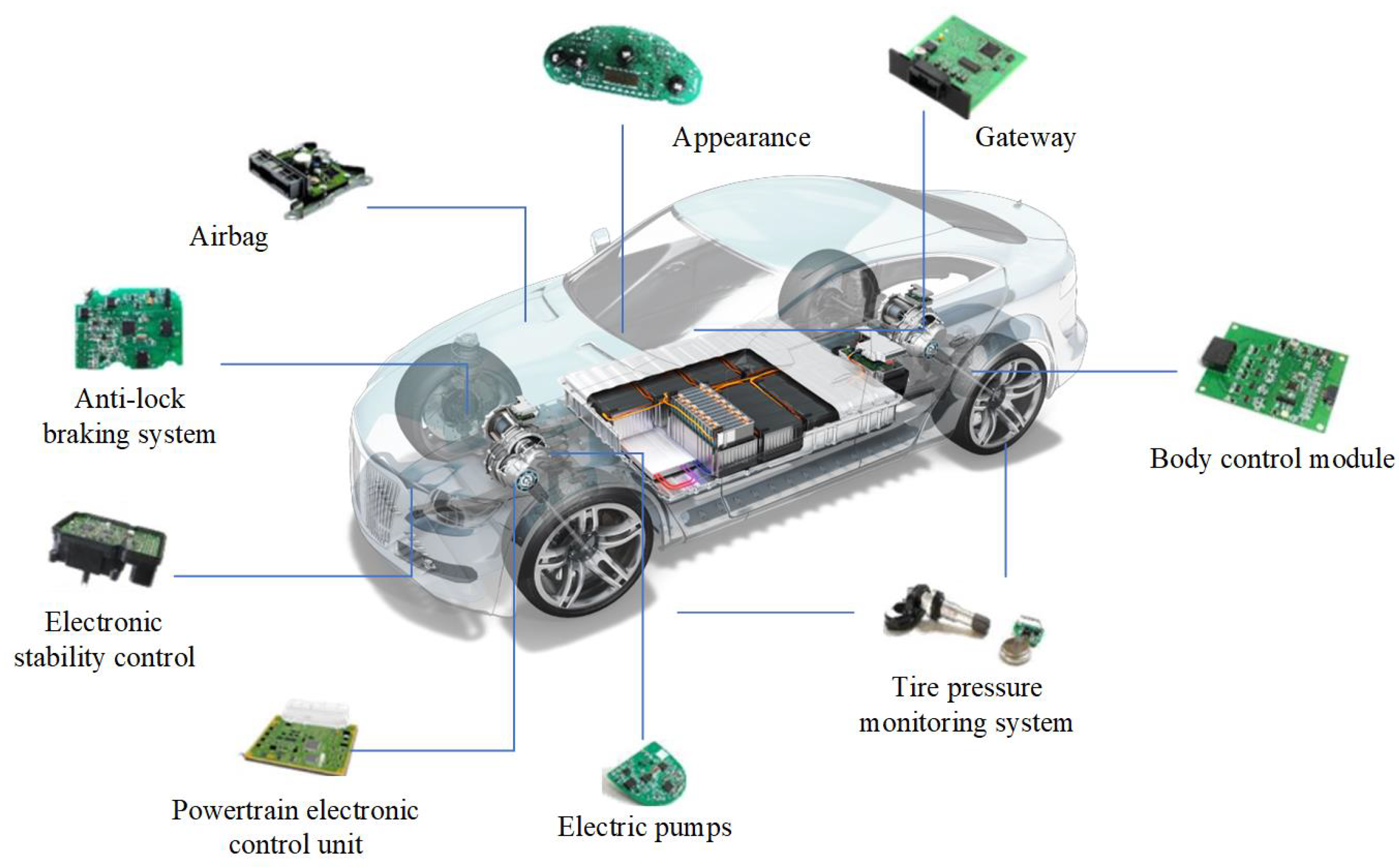
1. Introduction
2. Method Theory
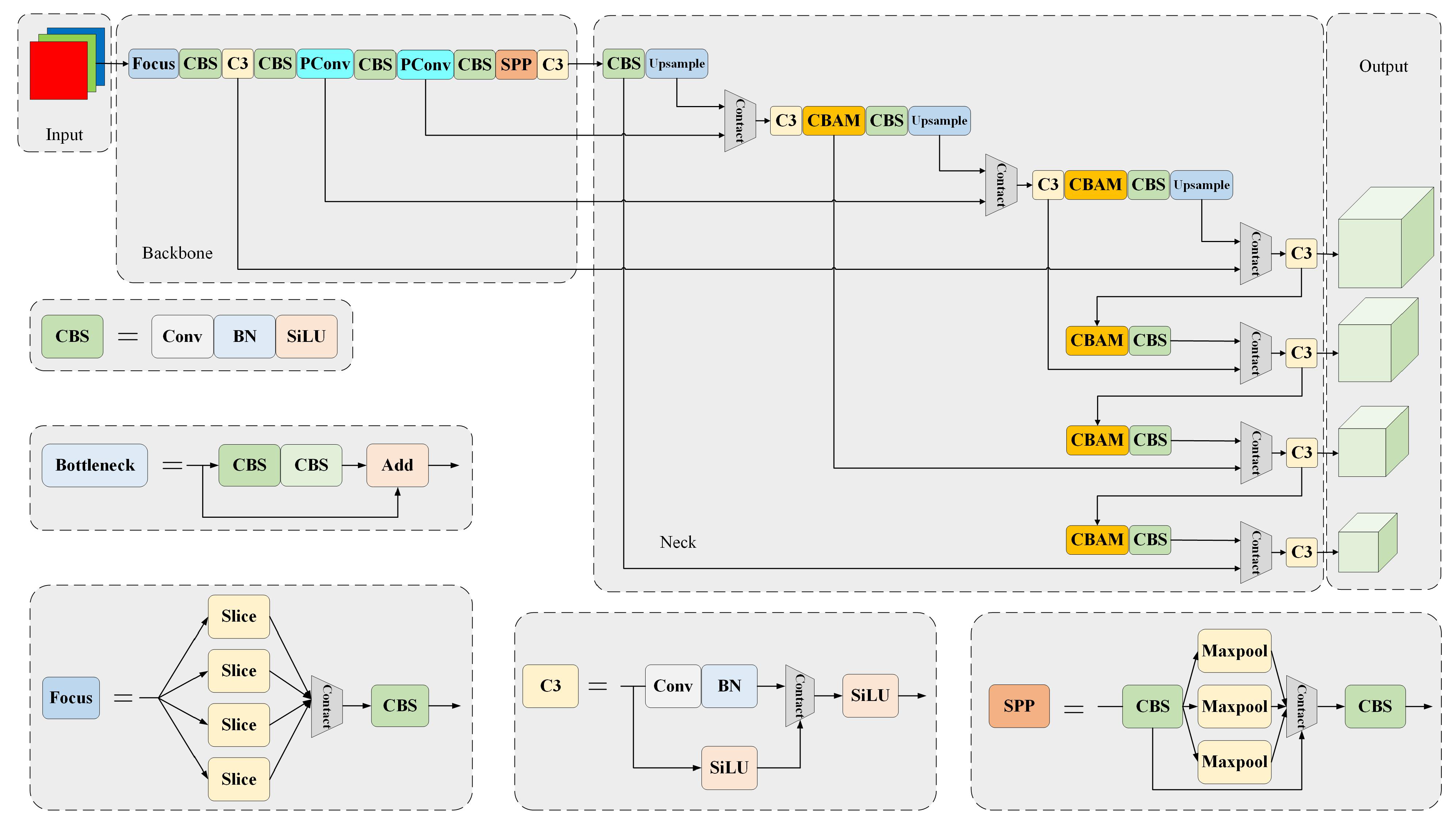
- Multi-scale fusion with CBAM attention mechanism: The integration of multi-scale fusion allows the model to incorporate feature maps from various resolutions, thereby enhancing its ability to recognize defects of different sizes. At the same time, the attention mechanism aids the model in capturing subtle features of these variations, improving the model’s generalization capabilities across diverse PCB samples;
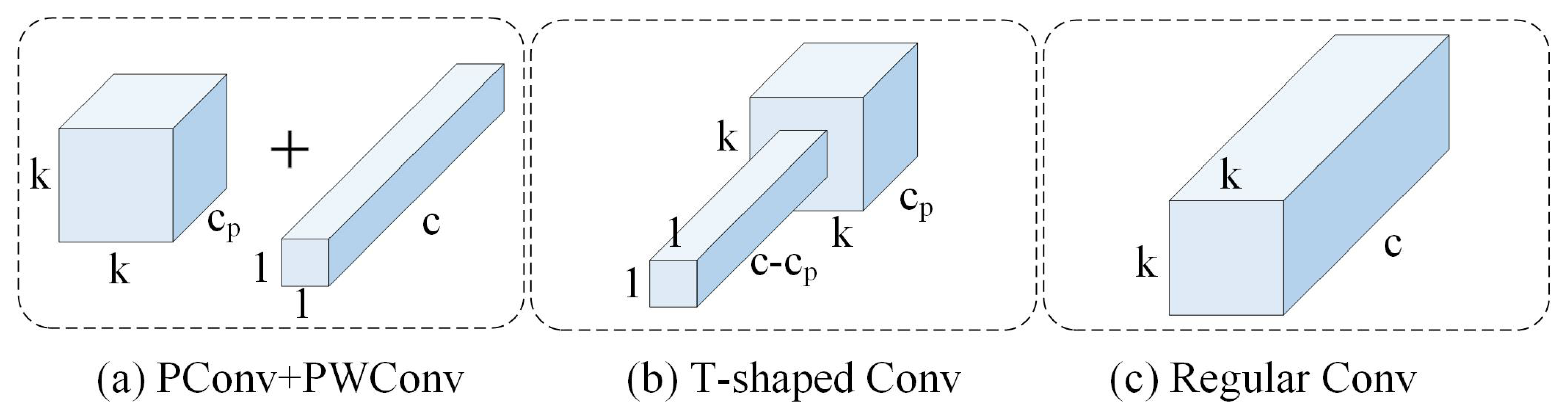
- Using partial convolution in the place of traditional convolution: Partial convolution is particularly effective in scenarios with irregular shapes or missing data, which is advantageous for detecting defects with unclear edges. Additionally, partial convolution reduces redundant computation and efficiently accesses memory, thereby enhancing the detection efficiency;
- Introduction of the NWD (normalized Wasserstein distance) loss function: The NWD loss provides smoother gradients, which helps avoid issues like gradient vanishing or exploding during the training process. Moreover, by more accurately measuring the differences between distributions, the NWD loss function aids in improving the model’s generalization ability for unseen data.
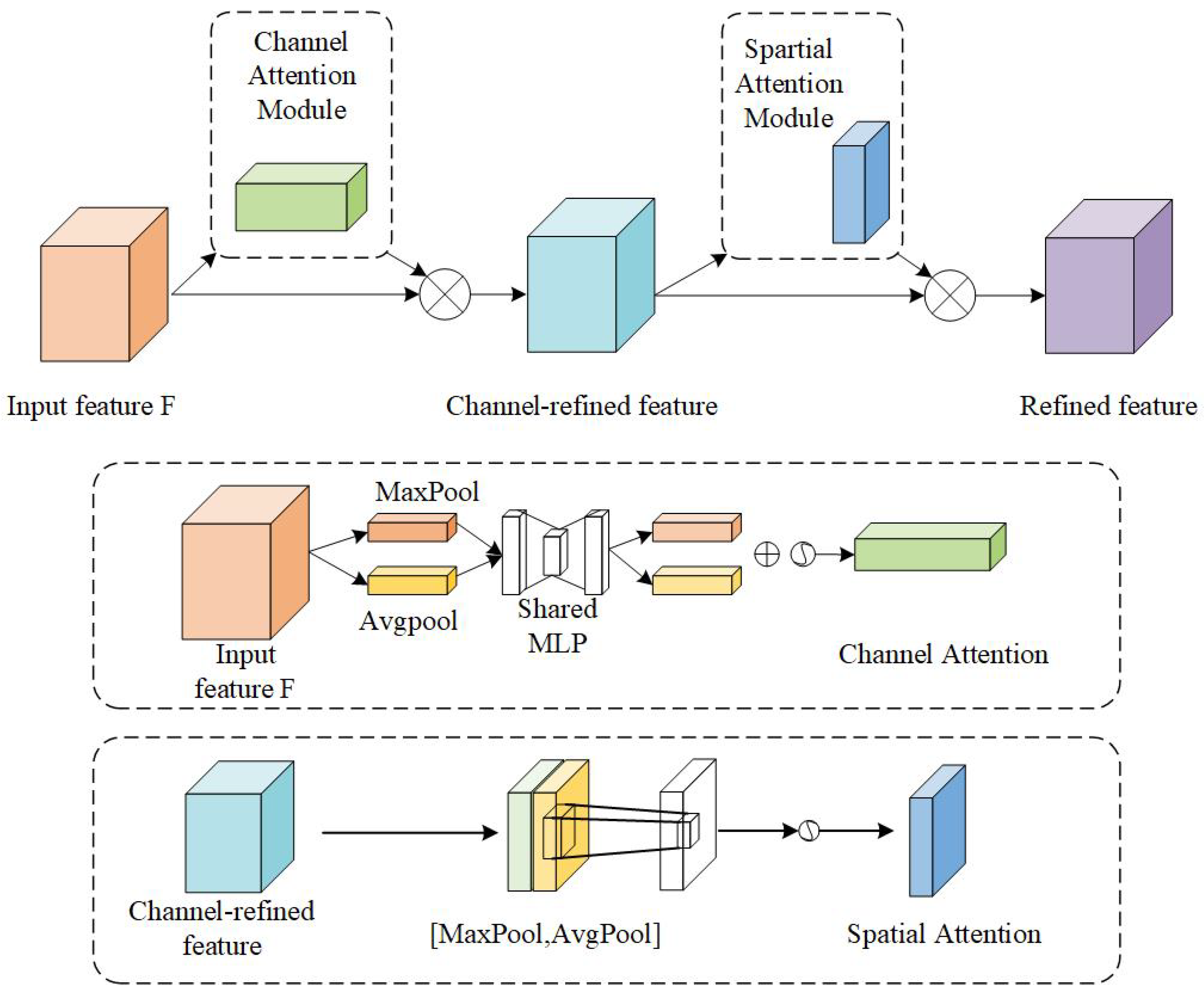
2.1. CBAM
2.2. PConv
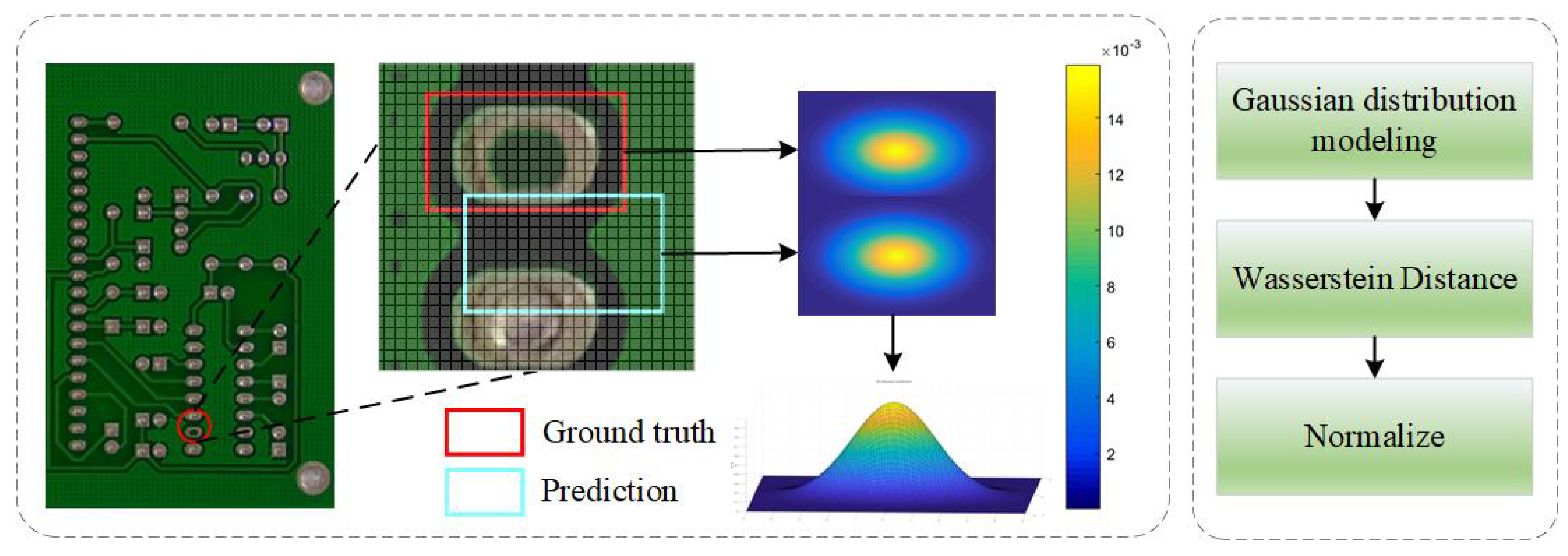
2.3. NWD Loss Function
3. Experimental Section
3.1. Data Set Processing and Training
3.2. Evaluation Metrics
3.3. Model Training
3.3.1. Model Results
3.3.2. Ablation Experiments
3.3.3. Model Comparison
4. Summary and Outlook
Author Contributions
Funding
Data Availability Statement
Conflicts of Interest
References
- Dunn, B.; Kamath, H.; Tarascon, J.M. Electrical Energy Storage for the Grid: A Battery of Choices. Science 2011, 334, 928–935. [Google Scholar] [CrossRef] [PubMed]
- Brooker, R.P.; Qin, N. Identification of potential locations of electric vehicle supply equipment. J. Power Sources 2015, 299, 76–84. [Google Scholar] [CrossRef]
- Lee, W.S.; Chang-Chien, G.P.; Wang, L.C.; Lee, W.J.; Tsai, P.J.; Wu, K.Y.; Lin, C. Source Identification of PCDD/Fs for Various Atmospheric Environments in a Highly Industrialized City. Environ. Sci. Technol. 2004, 38, 4937–4944. [Google Scholar] [CrossRef] [PubMed]
- IEEE Std 2030.1.1-2021 (Revision of IEEE Std 2030.1.1-2015)—Redline; IEEE Standard for Technical Specifications of a DC Quick and Bidirectional Charger for Use with Electric Vehicles—Redline. IEEE: Piscataway, NJ, USA, 2022; pp. 1–263.
- Li, J.; Gu, J.; Huang, Z.; Wen, J. Application Research of Improved YOLO V3 Algorithm in PCB Electronic Component Detection. Appl. Sci. 2019, 9, 3750. [Google Scholar] [CrossRef]
- Gu, X.; Ieromonachou, P.; Zhou, L. Subsidising an electric vehicle supply chain with imperfect information. Int. J. Prod. Econ. 2019, 211, 82–97. [Google Scholar] [CrossRef]
- Wu, H.; Lei, R.; Peng, Y. PCBNet: A Lightweight Convolutional Neural Network for Defect Inspection in Surface Mount Technology. IEEE Trans. Instrum. Meas. 2022, 71, 3518314. [Google Scholar] [CrossRef]
- Lu, Y.; Yang, B.; Gao, Y.; Xu, Z. An automatic sorting system for electronic components detached from waste printed circuit boards. Waste Manag. 2022, 137, 1–8. [Google Scholar] [CrossRef] [PubMed]
- Zeng, N.; Wu, P.; Wang, Z.; Li, H.; Liu, W.; Liu, X. A Small-Sized Object Detection Oriented Multi-Scale Feature Fusion Approach With Application to Defect Detection. IEEE Trans. Instrum. Meas. 2022, 71, 3507014. [Google Scholar] [CrossRef]
- Li, G.; Zhao, S.; Zhou, M.; Li, M.; Shao, R.; Zhang, Z.; Han, D. YOLO-RFF: An Industrial Defect Detection Method Based on Expanded Field of Feeling and Feature Fusion. Electronics 2022, 11, 4211. [Google Scholar] [CrossRef]
- Sezer, A.; Altan, A. Detection of solder paste defects with an optimization-based deep learning model using image processing techniques. Solder. Surf. Mt. Technol. 2021, 33, 291–298. [Google Scholar] [CrossRef]
- Kim, J.; Ko, J.; Choi, H.; Kim, H. Printed Circuit Board Defect Detection Using Deep Learning via A Skip-Connected Convolutional Autoencoder. IEEE Sens. Counc. 2021, 21, 4968. [Google Scholar] [CrossRef] [PubMed]
- Fridman, Y.; Rusanovsky, M.; Oren, G. ChangeChip: A Reference-Based Unsupervised Change Detection for PCB Defect Detection. In Proceedings of the 2021 IEEE Physical Assurance and Inspection of Electronics (PAINE), Washington, DC, USA, 30 November–2 December 2021; pp. 1–8. [Google Scholar]
- Hu, B.; Wang, J. Detection of PCB Surface Defects With Improved Faster-RCNN and Feature Pyramid Network. IEEE Accesss 2020, 8, 108335–108345. [Google Scholar] [CrossRef]
- Liao, X.; Lv, S.; Li, D.; Luo, Y.; Zhu, Z.; Jiang, C. YOLOv4-MN3 for PCB Surface Defect Detection. Appl. Sci. 2021, 11, 11701. [Google Scholar] [CrossRef]
- Xuan, W.; Jian-She, G.; Bo-Jie, H.; Zong-Shan, W.; Hong-Wei, D.; Jie, W. A Lightweight Modified YOLOX Network Using Coordinate Attention Mechanism for PCB Surface Defect Detection. IEEE Sens. J. 2022, 22, 20910–20920. [Google Scholar] [CrossRef]
- Xue, Z.; Lin, H.; Wang, F. A Small Target Forest Fire Detection Model Based on YOLOv5 Improvement. Forests 2022, 13, 1332. [Google Scholar] [CrossRef]
- Wan, G.; Fang, H.; Wang, D.; Yan, J.; Xie, B. Ceramic tile surface defect detection based on deep learning. Ceram. Int. 2022, 48, 11085–11093. [Google Scholar] [CrossRef]
- Wang, L.; Cao, Y.; Wang, S.; Song, X.; Zhang, S.; Zhang, J.; Niu, J. Investigation Into Recognition Algorithm of Helmet Violation Based on YOLOv5-CBAM-DCN. IEEE Access 2022, 10, 60622–60632. [Google Scholar] [CrossRef]
- Sun, Z.; Ibrayim, M.; Hamdulla, A. Detection of Pine Wilt Nematode from Drone Images Using UAV. Sensors 2022, 22, 4704. [Google Scholar] [CrossRef]
- Liu, G.; Dundar, A.; Shih, K.J.; Wang, T.C.; Reda, F.A.; Sapra, K.; Yu, Z.; Yang, X.; Tao, A.; Catanzaro, B. Partial Convolution for Padding, Inpainting, and Image Synthesis. IEEE Trans. Pattern Anal. Mach. Intell. 2023, 45, 6096–6110. [Google Scholar] [CrossRef]
- Chen, J.; Hong Kao, S.; He, H.; Zhuo, W.; Wen, S.; Lee, C.H.; Chan, S.H.G. Run, Don’t Walk: Chasing Higher FLOPS for Faster Neural Networks. In Proceedings of the 2023 IEEE/CVF Conference on Computer Vision and Pattern Recognition (CVPR), Vancouver, BC, Canada, 17–24 June 2023; pp. 12021–12031. [Google Scholar]
- Li, R.; Zhang, Y.; Niu, D.; Yang, G.; Zafar, N.; Zhang, C.; Zhao, X. PointVGG: Graph convolutional network with progressive aggregating features on point clouds. Neurocomputing 2021, 429, 187–198. [Google Scholar] [CrossRef]
- Pan, S.; Chen, K.; Chen, J.; Qin, Z.; Cui, Q.; Li, J. A partial convolution-based deep-learning network for seismic data regularization1. Comput. Geosci. 2020, 145, 104609. [Google Scholar] [CrossRef]
- Wang, J.; Xu, C.; Yang, W.; Yu, L. A Normalized Gaussian Wasserstein Distance for Tiny Object Detection. arXiv 2021, arXiv:2110.13389. [Google Scholar]
- Wang, Q.; Yang, L.; Zhou, B.; Luan, Z.; Zhang, J. YOLO-SS-Large: A Lightweight and High-Performance Model for Defect Detection in Substations. Sensors 2023, 23, 8080. [Google Scholar] [CrossRef] [PubMed]
- Zhang, J.; Wei, X.; Zhang, L.; Yu, L.; Chen, Y.; Tu, M. YOLO v7-ECA-PConv-NWD Detects Defective Insulators on Transmission Lines. Electronics 2023, 12, 3969. [Google Scholar] [CrossRef]
- Wang, Q.; Breckon, T. Unsupervised Domain Adaptation via Structured Prediction Based Selective Pseudo-Labeling. In Proceedings of the AAAI Conference on Artificial Intelligence, Honolulu, HI, USA, 27 January–1 February 2019. [Google Scholar]
- Bhowmik, N.; Wang, Q.; Gaus, Y.F.A.; Szarek, M.; Breckon, T. The Good, the Bad and the Ugly: Evaluating Convolutional Neural Networks for Prohibited Item Detection Using Real and Synthetically Composited X-ray Imagery. arXiv 2019, arXiv:1909.11508. [Google Scholar]
- Yang, Y.; Kang, H. An Enhanced Detection Method of PCB Defect Based on Improved YOLOv7. Electronics 2023, 12, 2120. [Google Scholar] [CrossRef]
- Du, B.; Wan, F.; Lei, G.; Xu, L.; Xu, C.; Xiong, Y. YOLO-MBBi: PCB Surface Defect Detection Method Based on Enhanced YOLOv5. Electronics 2023, 12, 2821. [Google Scholar] [CrossRef]
- Liu, J.; Cui, G.; Xiao, C. A real-time and efficient surface defect detection method based on YOLOv4. J. Real-Time Image Process. 2023, 20, 77. [Google Scholar] [CrossRef]


| Experimental Platform | Specific Model |
|---|---|
| CPU | Intel(R) Core(TM) i7-12700H |
| GPU | Nvidia GeForce RTX 3060 |
| Operating system | Windows 11 64 bit |
| Memory | 16 GB |
| Training framework | Pytorch |
| Multi-Scale CBAM | PConv | NWD | P/% | R/% | mAP/% |
|---|---|---|---|---|---|
| × | × | × | 96.07 | 93.14 | 95.68 |
| ✓ | × | × | 96.63 | 92.50 | 95.96 |
| × | ✓ | × | 97.63 | 95.97 | 97.64 |
| × | × | ✓ | 97.90 | 95.86 | 97.52 |
| ✓ | ✓ | ✓ | 96.77 | 96.33 | 98.13 |
| Model | P/% | R/% | mAP_0.5/% | mAP_0.5:0.95/% |
|---|---|---|---|---|
| SSD512 | 84.07 | 94.85 | 92.09 | 48.79 |
| YOLOv3 | 85.13 | 95.36 | 92.75 | 49.12 |
| YOLOv5s | 93.24 | 92.43 | 91.43 | 50.53 |
| YOLOv7 | 95.33 | 95.75 | 95.08 | 51.25 |
| Faster R-CNN | 90.51 | 86.48 | 89.23 | 49.87 |
| DenseNet | 87.35 | 97.46 | 94.12 | 51.39 |
| Proposed | 96.77 | 96.33 | 98.13 | 51.16 |
| Model | Missing Hole/% | Mouse Bite/% | Open Circuit/% | Short/% | Spur/% | Spurious Copper/% |
|---|---|---|---|---|---|---|
| Faster R-CNN | 90.3 | 91.6 | 90.8 | 89.6 | 88.5 | 92.4 |
| TDD-Net | 97.4 | 94.8 | 95.3 | 94.3 | 97.1 | 94.9 |
| YOLOv4 | 89.8 | 88.8 | 87.4 | 90.6 | 89.8 | 93.3 |
| YOLOv5s | 90.7 | 95.3 | 91.9 | 87.4 | 96.5 | 94.6 |
| YOLOv7 | 98.3 | 93.2 | 94.9 | 93.1 | 97.2 | 95.4 |
| YOLO-MBBi [31] | 98.5 | 95.3 | 96.0 | 91.8 | 97.6 | 95.6 |
| Proposed | 98.5 | 96.0 | 98.3 | 96.6 | 96.9 | 97.3 |
| Model | Missing Hole/% | Mouse Bite/% | Open Circuit/% | Short/% | Spur/% | Spurious Copper/% |
|---|---|---|---|---|---|---|
| Faster R-CNN | 87.0 | 84.8 | 86.7 | 90.1 | 83.3 | 86.1 |
| TDD-Net | 98.4 | 92.6 | 97.8 | 96.2 | 92.5 | 95.2 |
| YOLOv4 | 91.2 | 83.1 | 87.1 | 90.4 | 81.1 | 90.1 |
| YOLOv5s | 91.3 | 90.8 | 96.7 | 92.6 | 90.0 | 95.6 |
| YOLOv7 | 98.9 | 92.1 | 98.8 | 95.1 | 93.3 | 95.7 |
| YOLO-MBBi [31] | 98.9 | 92.5 | 97.2 | 93.4 | 90.0 | 95.7 |
| Proposed | 100 | 90.3 | 96.5 | 95.3 | 95.8 | 94.5 |
| Model | Missing Hole/% | Mouse Bite/% | Open Circuit/% | Short/% | Spur/% | Spurious Copper/% |
|---|---|---|---|---|---|---|
| Faster R-CNN | 85.5 | 88.2 | 89.5 | 90.6 | 90.2 | 91.4 |
| TDD-Net | 97.1 | 94.5 | 97.2 | 91.9 | 94.0 | 95.7 |
| YOLOv4 | 86.0 | 82.8 | 85.3 | 91.4 | 86.0 | 94.8 |
| YOLOv5s | 85.8 | 94.2 | 93.5 | 89.8 | 93.8 | 92.9 |
| YOLOv7 | 97.7 | 94.0 | 97.6 | 91.8 | 94.3 | 96.2 |
| YOLO-MBBi [31] | 97.6 | 94.5 | 97.3 | 92.1 | 94.5 | 95.7 |
| Proposed | 99.3 | 95.9 | 99.2 | 97.0 | 99.2 | 97.6 |
Disclaimer/Publisher’s Note: The statements, opinions and data contained in all publications are solely those of the individual author(s) and contributor(s) and not of MDPI and/or the editor(s). MDPI and/or the editor(s) disclaim responsibility for any injury to people or property resulting from any ideas, methods, instructions or products referred to in the content. |
© 2024 by the authors. Licensee MDPI, Basel, Switzerland. This article is an open access article distributed under the terms and conditions of the Creative Commons Attribution (CC BY) license (https://creativecommons.org/licenses/by/4.0/).
Share and Cite
Xu, H.; Wang, L.; Chen, F. Advancements in Electric Vehicle PCB Inspection: Application of Multi-Scale CBAM, Partial Convolution, and NWD Loss in YOLOv5. World Electr. Veh. J. 2024, 15, 15. https://doi.org/10.3390/wevj15010015
Xu H, Wang L, Chen F. Advancements in Electric Vehicle PCB Inspection: Application of Multi-Scale CBAM, Partial Convolution, and NWD Loss in YOLOv5. World Electric Vehicle Journal. 2024; 15(1):15. https://doi.org/10.3390/wevj15010015
Chicago/Turabian StyleXu, Hanlin, Li Wang, and Feng Chen. 2024. "Advancements in Electric Vehicle PCB Inspection: Application of Multi-Scale CBAM, Partial Convolution, and NWD Loss in YOLOv5" World Electric Vehicle Journal 15, no. 1: 15. https://doi.org/10.3390/wevj15010015
APA StyleXu, H., Wang, L., & Chen, F. (2024). Advancements in Electric Vehicle PCB Inspection: Application of Multi-Scale CBAM, Partial Convolution, and NWD Loss in YOLOv5. World Electric Vehicle Journal, 15(1), 15. https://doi.org/10.3390/wevj15010015