Article

Analysis of the THD and Common-Mode Voltage of the Three-Phase Boost-Buck EV Traction Inverter

1
School of Automotive Studies, Tongji University, Shanghai 201804, China
2
School of Mechatronic Engineering and Automation, Shanghai University, Shanghai 200444, China
*
Author to whom correspondence should be addressed.
World Electr. Veh. J. 2022, 13(7), 114; https://doi.org/10.3390/wevj13070114
Submission received: 30 May 2022 / Revised: 22 June 2022 / Accepted: 23 June 2022 / Published: 27 June 2022
(This article belongs to the Special Issue Modern Charging Techniques for Electrical Vehicles)

Abstract

:
A three-phase boost-buck inverter (BBI) comprised of three identical boost-buck DC/DC converter modules is presented for an EV traction inverter application. It allows the step-up and/or step-down of the battery pack voltage according to the operating condition of the traction motor so that the overall performance can be optimized, which is essential for EVs with relatively low and varying battery voltages such as a hybrid EV or fuel-cell EV. It also features low switching losses, low harmonic distortion in the output current, and reduced common-mode voltage and/or current. A detailed analysis and performance evaluation of the BBI compared to the conventional technology demonstrate its feasibility in EV traction applications. The functionality and performance of the boost-buck inverter are verified with simulation and experimental results.

1. Introduction

Traction inverters in Electric Vehicles (EV) have to handle wide operating ranges of the motor corresponding to the complex driving cycle characteristics. The battery voltage also varies depending on the state-of-charge of the widely adopted lithium-ion batteries. In fuel cell (FC)-type EVs, the terminal voltage of the FC stack typically varies in a wide range depending on the load condition. EV motors operate in wide speed and torque ranges, which requires the traction inverter to operate reliably in wide voltage and current ranges. In order to reduce the energy consumption and increase mileage, it is critical for the inverter to be highly efficient under different loading conditions [1,2,3,4,5,6].
The conventional two-level voltage source inverter (VSI) is widely used in motor drive applications. It has a simple structure and low parts count, which translates into a lower cost and higher reliability. However, the high-power requirement of the EV motor drive still requires paralleling multiple semiconductor power devices either at the chip level or at the power module level [7,8]. The main constraint of this topology is that it only has buck-type functionality, i.e., the amplitude of the ac line-to-line voltage is always lower that the dc input (battery pack) voltage. In the high-speed range of the EV motor, due to the limited output voltage amplitude, field-weakening control is usually adopted to increase the motor speed. However, field-weakening control has the disadvantages of reduced driving torque, higher torque ripple, complicated control, and possible demagnetization of the permanent magnets [9,10,11].
A two-stage topology, as shown in Figure 1a, consists of a bidirectional boost/buck converter and a VSI, denoted as B-VSI hereafter, has been proposed to enable voltage step-up functionality [1,2,3]. The dc link voltage can be controlled by the boost converter according to the operating condition of the motor. The design of the battery pack and the motor can then be decoupled so that the system performance can be optimized [12,13]. The operating range of the inverter and the motor is extended, and the motor control in the high-speed range can be simplified. For the control of the inverter, a conventional space vector PWM (SVPWM) is typically used due to its low total harmonic distortion (THD) of the three-phase output current. However, as the B-VSI is essentially a two-stage topology, more power losses are generated in the switching devices, resulting in a lower efficiency of the inverter.
The THD of the Inverter output current is relevant as it directly affects the torque ripple, noise, and eddy current losses in the motor [14,15,16,17,18,19,20,21,22]. The THD can be reduced by simply increasing the switching frequency. However, due to efficiency requirements and the constraints on the cost and size of the cooling system, the switching frequency of the power switches in the traction inverter is typically limited to a few kilohertz (kHz). Wide-band-gap (WBG) semiconductor power devices such as SiC MOSFETs enable a higher switching frequency due to its much faster switching speed (high dv/dt) and lower switching losses [23]. However, the application of WBG devices exacerbates the challenges associated with a high dv/dt and common-mode (CM) voltage and/or current. CM current or leakage current will be induced by the CM voltage due to the distributed stay capacitances between the winding and the ground [24,25,26]. The leakage current flows through the motor bearings and may cause damage, which is a major reliability issue [27,28,29].
A three-phase dc/ac inverter based on modular boost-buck dc/dc converters, denoted as BBI, has been studied in the literature [30]. The BBI has voltage buck and boost functionality and high efficiency. Its operating principle and device loss characteristics have been analyzed, and its efficiency has been evaluated with simulation results. However, detailed analysis of the THD and CM voltage/current characteristics of the BBI has not been found in the literature. This article serves to fill this gap and presents extensive analysis with simulation and experimental validation, including a performance comparison between the BBI and the B-VSI. An interleaving method is also designed so that the ripple in the input current can be reduced.
The operation principle of the BBI is first described in Section 2 to facilitate further analyses. Detailed analysis of the CM voltage and current, THD of the output current, and the design of an interleaving method are presented in Section 3. The analyses are verified by extensive simulation results in Section 4, with the performance comparison between the BBI and B-VSI. Experimental results based on a scaled-down hardware prototype are shown in Section 5, which validates the performance of the BBI. Finally, the conclusions are given in Section 6.

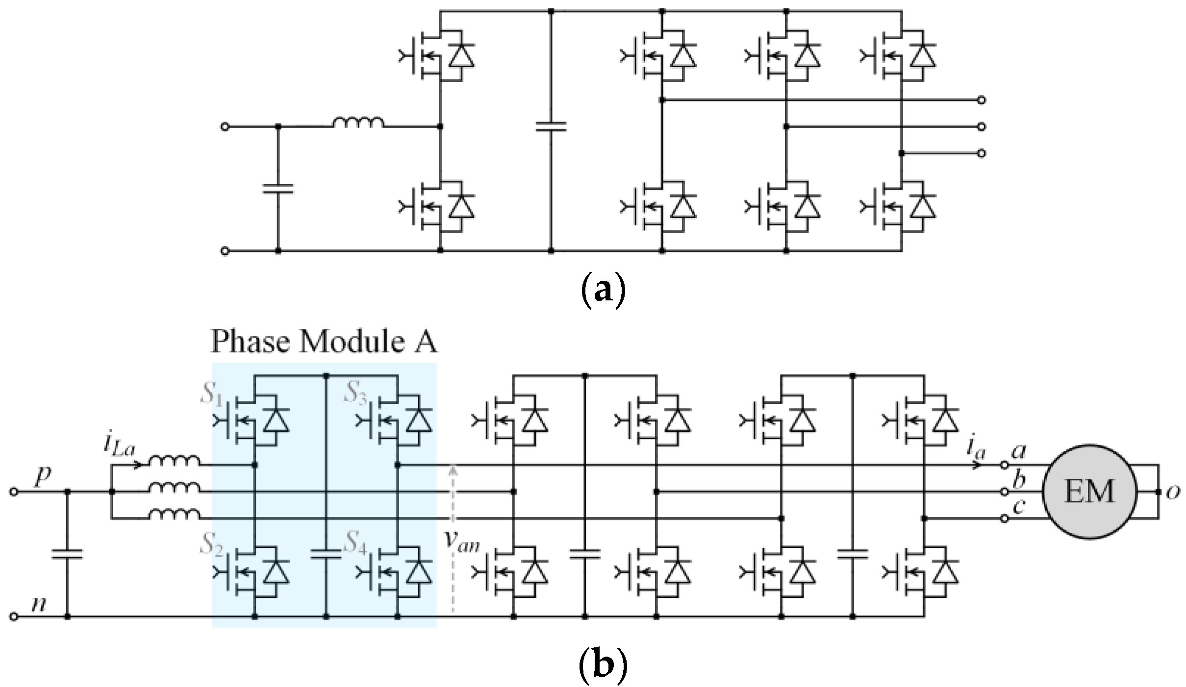
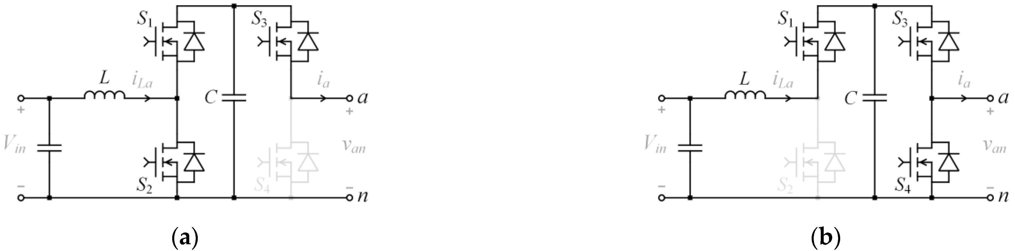
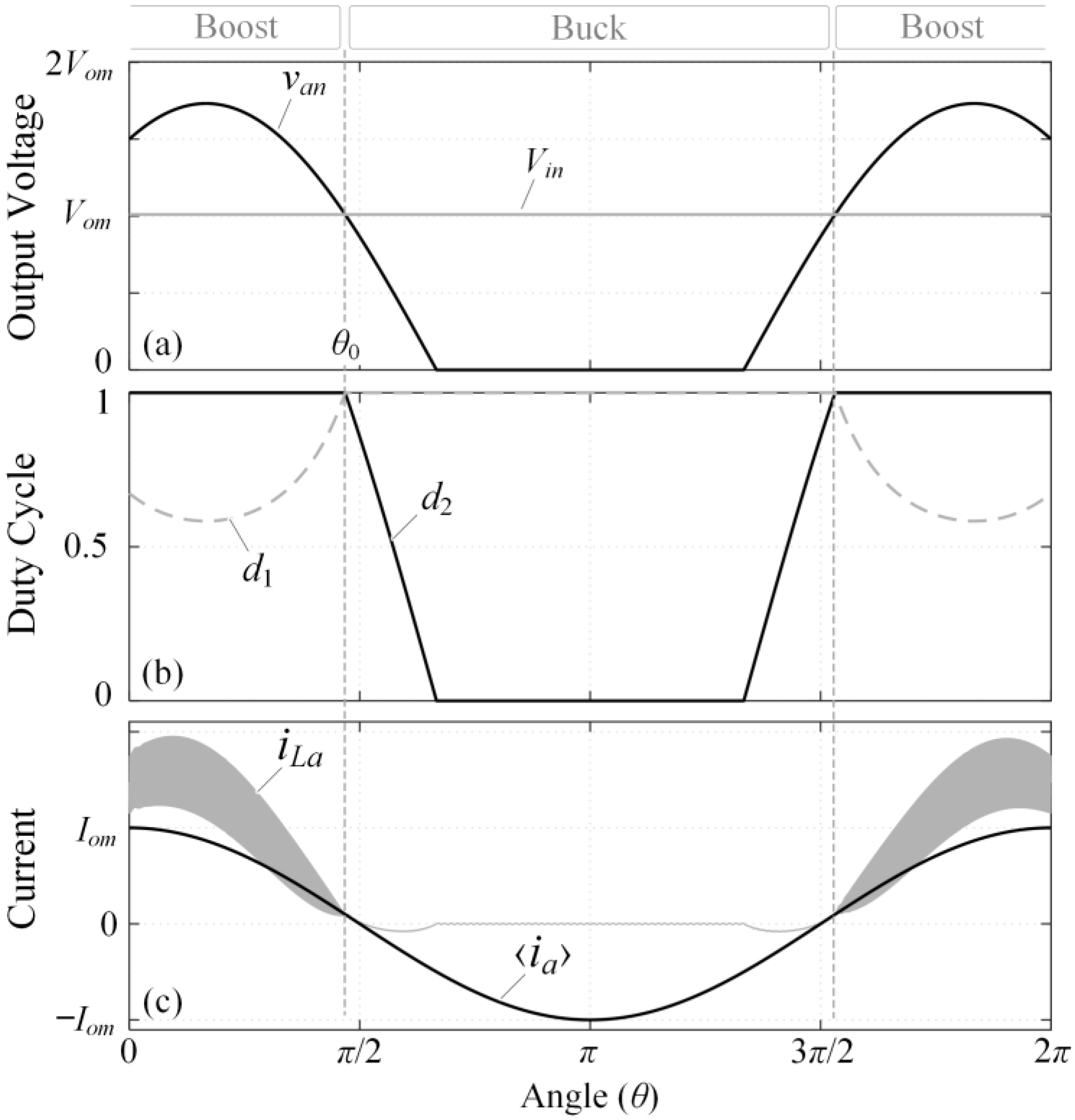
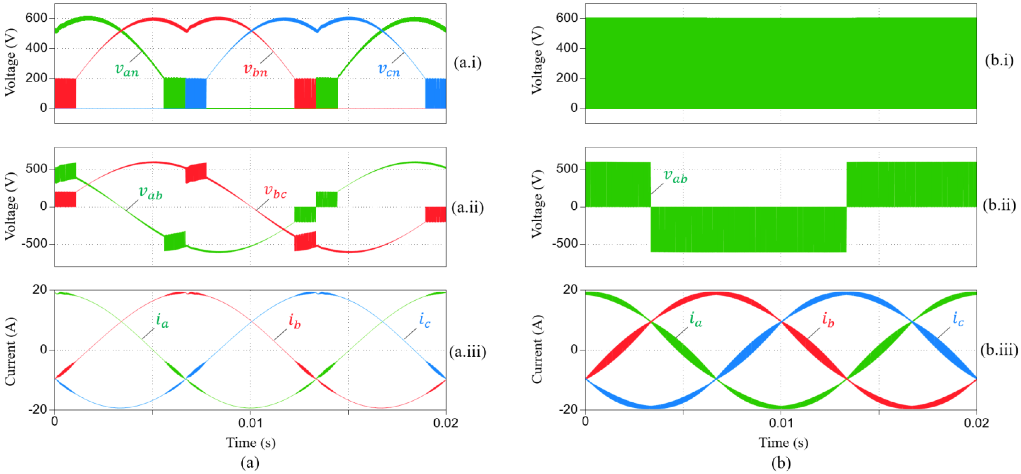
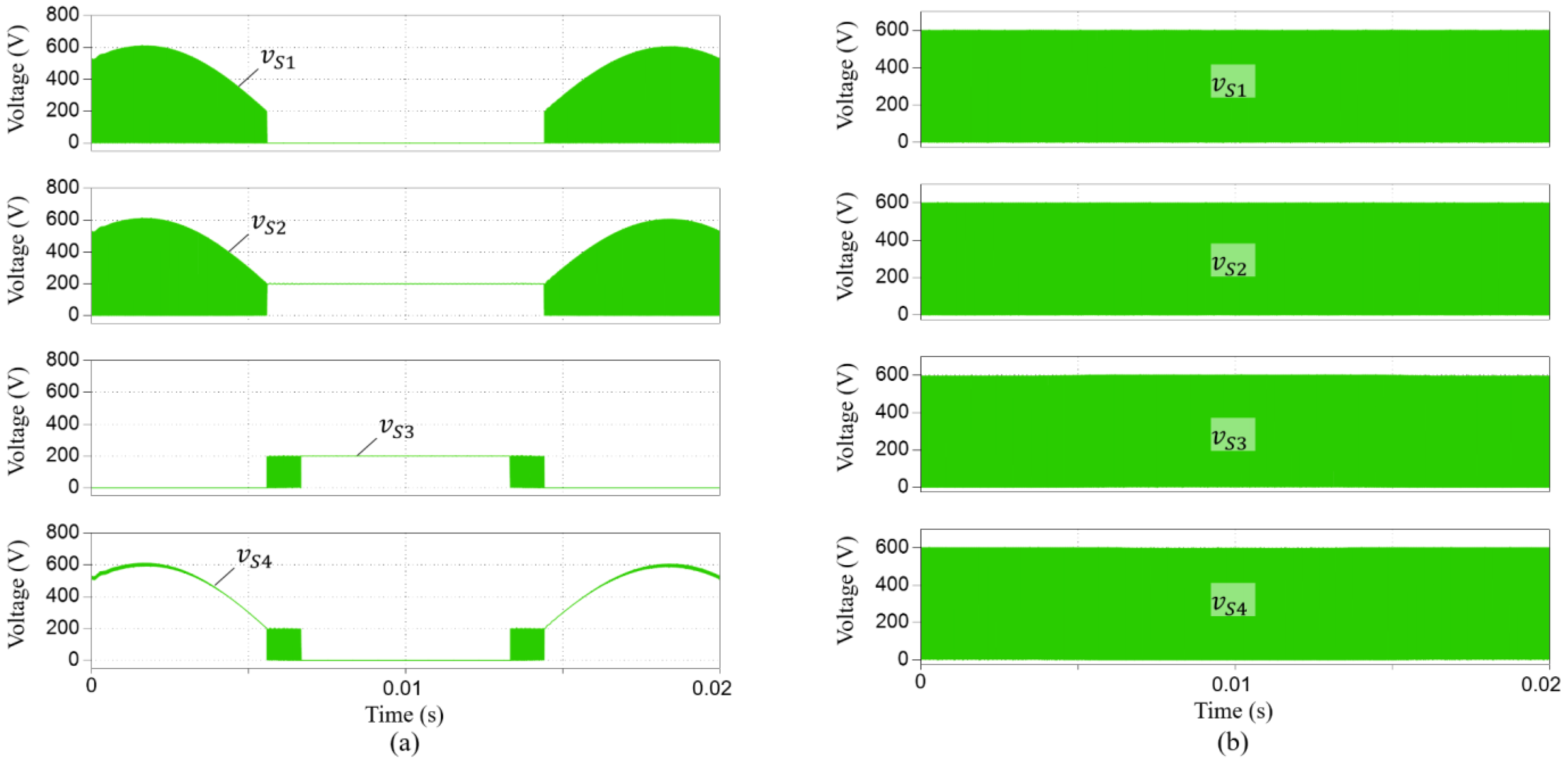
2. Operating Principle

The basic operating principle of the BBI has been described in the literature [30]. It is briefly summarized here to facilitate further analyses and discussions. The BBI topology is shown in Figure 1b. Each phase module of the inverter is a boost-buck converter consisting of two switch legs. The three phase modules are the same, and phase A is explained in detail. The switch leg S1–S2, together with the input inductor L, forms a boost converter. The switch leg S3–S4 forms a buck converter.
The operation modes of phase module A in the BBI are illustrated in Figure 2. When the reference for the phase voltage v a n is lower than the input voltage V i n , the phase modules operate as a buck converter. S1 is always turned-on and S2 is always turned-off, i.e., the boost switch leg has no switching actions. The buck switch leg is controlled in pulse width modulation (PWM) mode with duty cycle d2 for S3.
When the reference for the phase voltage v a n is higher than the input V i n , the phase modules operate as a boost converter. S3 is always turned-on and S4 is always turned-off, i.e., the buck switch leg has no switching actions. The boost switch leg is controlled in pulse width modulation (PWM) mode with duty cycle d1 for S1. In this mode, the output voltage is filtered by the dc link capacitor of the phase module.
The phase-modules are dc/dc converters that generate positive output voltages consisting of a sinusoidal component and a dc bias:
v a n = V o m cos ( ω 1 t ) + v b i a s
v b n = V o m cos ( ω 1 t 2 π 3 ) + v b i a s
v c n = V o m cos ( ω 1 t + 2 π 3 ) + v b i a s
where V o m and ω 1 are the amplitude and angular frequency of the fundamental output voltage of the inverter, respectively. It is assumed that the load has a unity power factor. The overall modulation index is expressed as
M = 2 V o m V i n
which describes the combined effect of the voltage gain of the boost stage and the modulation depth of the buck (inverter) stage. Due to symmetry of the three phases, only the analysis of phase A is described here.
The discontinuous pulse width modulation (DPWM) strategy is implemented by a bias voltage expressed as
v b i a s ( t ) = min [ v a o ( t ) , v b o ( t ) , v c o ( t ) ]
The operating waveforms of the BBI with the DPWM strategy are shown in Figure 3. Among the three buck switch legs of the three phases, the phase with the most negative reference voltage is clamped to the negative dc bus for one third of the fundamental period. Therefore, the number of switching actions and the associated switching losses are significantly reduced compared to continuous PWM methods such as the conventional SVPWM.
As the waveforms are symmetrical about θ = ω 1 t = π , the expressions are derived only for the interval θ ( 0 ,   π ] . The operation of the phase module switches between the buck mode and the boost mode, as shown in Figure 3. By equating the reference voltage and the input voltage, the boundary phase angle between the two modes can be solved and is expressed as
θ o = acos ( 2 3 M ) + π 6
Based on the characteristics of the buck and boost converter, the control duty cycles for the two switch legs can be expressed as
d 1 ( θ ) = { 2 3 M cos ( θ π / 6 ) , θ ( 0 , θ o ] 1 , θ ( θ o , π ]
d 2 ( θ ) = { 1 , 3 M cos ( θ π / 6 ) 2 , 0 , θ ( 0 , θ o ] θ ( θ o , 2 π / 3 ] θ ( 2 π / 3 , π ]

3. CM Voltage, THD, and Interleaving Method

The CM voltage and/or current, THD of the output current, and characteristics of the input current are important factors for the design of a traction inverter. Characteristics of the relevant waveforms are analyzed, and analytical expressions are derived in the following, which can be used for the design and control of the inverter.

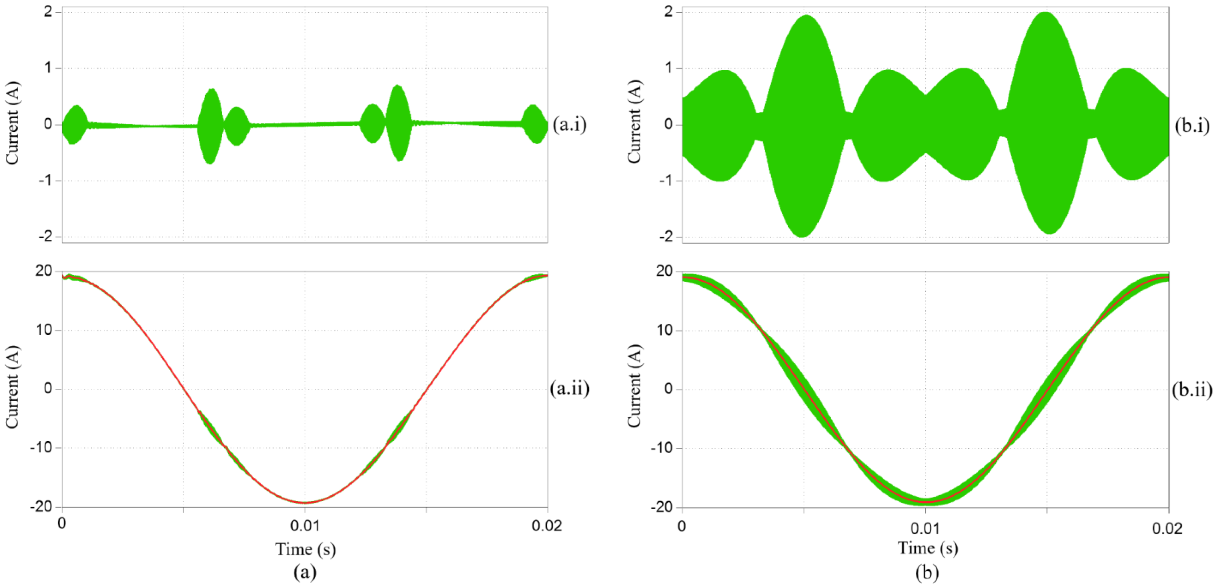
3.1. CM Voltage and Current

In motor drive applications, leakage current is induced by the CM voltage due to the high dv/dt of the switching actions and the parasitic elements in the system. The parasitic elements in the electric machines are mainly capacitive due to the large surface area of the windings and the frame, and the small distance between them. The influence of the CM voltage mainly depends on dv/dt and the magnitude of the CM voltage.
Figure 4 illustrates the characteristic waveforms of the output voltages of the three phases (van, vbn, and vcn, referenced to the negative dc rail), as well as the CM voltage vCM that is equal to the load neutral voltage von, i.e.,
v CM = v o n = ( v a n + v b n + v c n ) / 3
The waveforms of the output voltages are smooth during the boost mode of the phase modules. The corresponding CM voltage waveform is also smooth when at least two phase modules are in boost mode, which means it does not excite dv/dt-related high-frequency leakage current.
The CM voltage only presents a pulsed pattern when any of the phase modules is in buck mode. For the BBI, the magnitude of the voltage level shift V C M P of the CM voltage pulses is directly related to the lower input voltage, i.e.,
V C M P , B B I = V i n / 3
For the B-VSI, it is directly related to the boosted dc-link voltage, i.e.,
V C M P , B V S I = V d c l i n k / 3
Moreover, as the high-frequency pulses occur only in buck mode of the BBI, the average switching frequency corresponding to the high-frequency CM voltage and/or current can be expressed as
f s w , C M = 2 ( 2 π 3 θ 0 ) 2 π 3 f s w
For the B-VSI, as the three phases are constantly switching when the conventional space vector modulation is used, the average switching frequency is the same as f s w . The amplitude of the leakage current pulses is approximately proportional to V C M P , and the number of leakage current pulses over a fundamental cycle is proportional to f s w , C M . The ratio of the RMS leakage current of the BBI to that of the B-VSI, at the same load voltage and power level, can be approximated as
I C M , B B I I C M , B V S I V i n f s w , C M V d c l i n k f s w
When the commanded output voltage is relatively low ( M < 2 / 3 ), the boost stage is bypassed, and V d c l i n k = V i n so that
I C M , B B I I C M , B V S I f s w , C M f s w
When the commanded output voltage is relatively high ( M 2 / 3 ), the highest utilization of the dc link voltage is usually adopted, i.e., V d c l i n k = 3 V o m , neglecting nonideal effects such as device voltage drop, dead-band time, and design margin, etc. Equation (13) can then be expressed as
I C M , B B I I C M , B V S I V i n f s w , C M 3 V o m f s w = 2 3 M f s w , C M f s w
Therefore, it is concluded that the high-frequency leakage current generated by the BBI is always smaller than that with the B-VSI. The reduction is more significant when the output voltage, i.e., the overall modulation index M, is high.

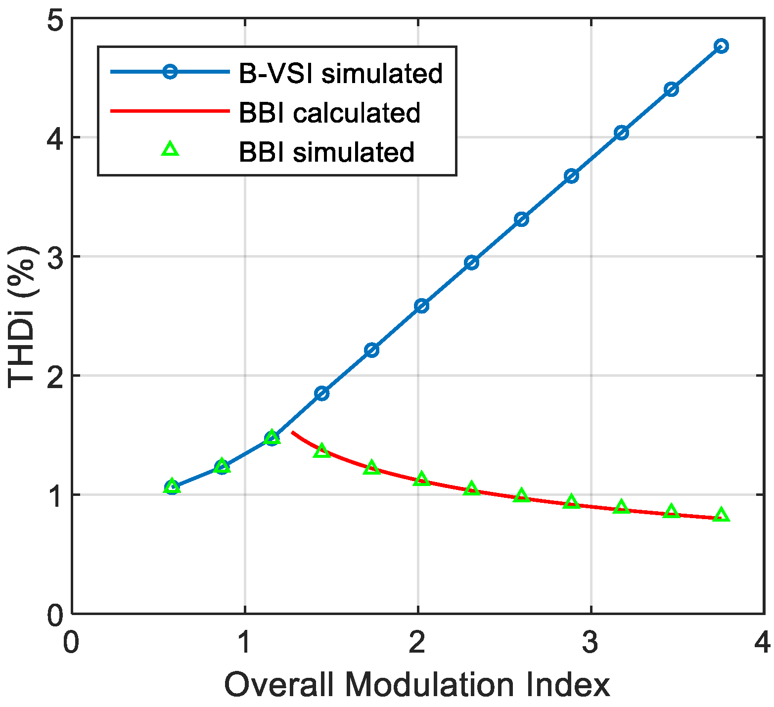
3.2. THD of the Output Current

Figure 5 illustrates the characteristic waveforms of phase A of the BBI, specifically, the phase module output voltage van, the load neutral voltage von with respect to the negative dc rail, the load phase voltage vao = vanvon, and the load phase current ia. Note that these waveforms follow the same pulse pattern during the buck mode.
During the boost mode, the load ripple current is negligible thanks to the inherent filtering effect of the dc-link capacitors. During the buck mode—for instance, θ [ θ 0 , 2 π 3 ] —the characteristic of the load ripple current is the same as that of the inductor current in a buck converter. As the magnitude of the pulsating component of the CM voltage is V i n / 3 , the magnitude of the pulsating voltage across the load inductance L M is, therefore, equal to 2 V i n / 3 . The peak-to-peak ripple in the load current can be expressed as
Δ i ( θ ) = Δ I n d 2 ( θ ) ( 1 d 2 ( θ ) ) ,   θ [ θ 0 , 2 π 3 ]
Δ I n = 2 V i n 3 L M f s w
Due to symmetry, the RMS ripple current over a fundamental cycle can be calculated as
Δ I r m s = 1 π 0 π Δ i r m s 2 ( θ ) d θ
where Δ i r m s 2 ( θ ) is the local RMS of the ripple current and, during the phase interval of θ [ θ 0 , 2 π 3 ] , it can be expressed as
Δ i r m s 2 ( θ ) = Δ i 2 ( θ ) 12 ,   θ [ θ 0 , 2 π 3 ]
Due to symmetry of the three-phase waveforms and the characteristic of the CM voltage, the magnitude of the load inductance voltage over the phase intervals θ [ 0 , 2 π 3 θ 0 ] and θ [ 2 π 3 , 4 π 3 θ 0 ] is equal to half of that during θ [ θ 0 , 2 π 3 ] . Therefore, the RMS ripple current can be expressed as
Δ I r m s = 1 π θ 0 2 π 3 Δ i r m s 2 ( θ ) [ 2 ( 1 2 ) 2 + 1 ] d θ
Substituting Equations (16), (17), and (19) into (20), we have
Δ I r m s = Δ I n 8 π θ 0 2 π 3 [ d 2 ( θ ) ( 1 d 2 ( θ ) ) ] 2 d θ
The exact closed-form expression for the RMS ripple current is unfeasible due to the form of transcendental equations in the solution of the integration in (21). However, it can be numerically calculated to guide the selection of the switch devices. Nonetheless, the duty ratio d 2 can be approximated by a linear relationship with θ , i.e.,
d 2 ( θ ) θ θ 0 2 π 3 θ 0 ,   θ [ θ 0 , 2 π 3 ]
An approximate closed-form expression of Δ I r m s can be obtained by substituting Equation (22) into (21), and with some simplification, i.e.,
Δ I r m s Δ I n 8 π 2 π 3 θ 0 30
Substituting Equations (6) and (17) into (23), an expanded expression can be obtained as
Δ I r m s V i n 6 15 π L M f s w π 2 acos ( 2 3 M )
The THD of the load current can then be calculated as
T H D i = Δ I r m s I r m s , 1
where I r m s , 1 is the fundamental RMS current. It can be concluded from Equation (24) that the THDi of the BBI will decrease as the overall modulation index M increases. This is because a higher M means a higher output voltage, which, in turn, means a wider duration of the boost operation mode of the BBI, and the inherent filtering effect becomes more significant.
It is noted that the derived expressions apply in the modulation index range of M > 4 / 3 , in which the phase-module switches between two modes only once during a half cycle. In the modulation index range of M ( 0 ,   2 / 3 ] , the boost switch leg is always clamped, and the BBI works the same way as the conventional three-phase two-level inverter, of which the THDi expression has been derived in the literature. In the modulation index range of M ( 2 / 3 ,   4 / 3 ] , the phase-module switches between the two modes more than once during a half cycle. However, the derived expressions can still be applied as an approximation, as the modulation index is within a narrow band close to 4/3.

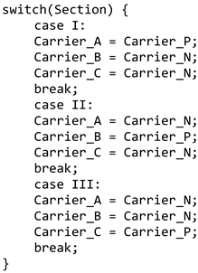
3.3. Phase Swapping Interleaving Method

The fundamental cycle can be divided into three sections, i.e., Section I: θ ( 0 ,   2 π / 3 ] ; Section II: θ ( 2 π / 3 ,   4 π / 3 ] ; Section III: θ ( 4 π / 3 ,   2 π ] . During each of these sections, only two out of the three phase modules are actively operating, while the third one is in clamping mode. Specifically, in Section I, phases A and B are operating and phase C is clamped. In Section II, phases B and C are operating and phase A is clamped. In Section III, phases C and A are operating and phase B is clamped. Based on this pattern, a phase swapping interleaving method for the boost switch-legs is designed so that the input inductor ripple current of the active phase modules is out of phase and the ripple of the total input current can be reduced.
Let Carrier_P and Carrier_N denote two triangular carrier signals of the switching frequency and opposite phase, respectively. Let Carrier_A, Carrier_B, and Carrier_C denote the triangular carrier signals for the boost switch-legs of phases A, B and C, respectively. The phase swapping-interleaving method is implemented by the following pseudo-code.
Wevj 13 00114 i001
Carrier_A, Carrier_B, and Carrier_C are then used together with the corresponding control signals to generate the control pulses for the boost switch-legs.

4. Simulation Evaluation

The performance of the BBI is simulated in PLECS and compared against the B-VSI. The two topologies are based on the circuit configuration shown in Figure 1b. The B-VSI is implemented by connecting the positive rails of the three modules so that the three boost legs are operating in parallel. The circuit parameters of the simulated inverter are the same as the scaled-down 10 kW hardware prototype and is shown in Table 1. The BBI is controlled with DPWM while the B-VSI is controlled with conventional SVPWM. The load motor is represented by series-connected resistors and inductors, which do not influence the evaluation of the inverter.
Figure 6 shows the characteristic voltage and current waveforms of the two topologies under the same operating condition. The corresponding overall modulation index is M = 3.46. The output voltages of the phase modules of the BBI demonstrate its two operating modes during a fundamental cycle. For instance, van is a pulse-width-modulated voltage when the commanded value is lower than the input voltage (buck mode), and it is a filtered smooth waveform when the commanded value is higher than the input voltage (boost mode). The resulting line-to-line voltage is a partially filtered waveform with drastically lower high-frequency harmonics than that with the B-VSI. The total harmonic distortion of the output current (THDi) obtained by the BBI is only 0.85%, 5.2 times lower than the THDi value of 4.40% with the B-VSI.
Figure 7 shows a direct comparison of the ripple component in the current waveforms of the two topologies. With the inherent filter characteristic, the current waveform with the BBI is smooth during most of the fundamental cycle and the peak ripple current is only 0.6 A (3.1% of the fundamental component). In comparison, high-frequency ripple current is present throughout the fundamental cycle with the B-VSI with a peak value of 2.0 A (10.2% of the fundamental component).
Figure 8 shows the comparison of the THD of the output current of the two topologies at different overall modulation indexes M. When M  2 / 3 , i.e., the peak value of the output line-to-line voltage Vllm is not greater than the input voltage Vin, the boost switch-legs are bypassed. The BBI is the same as the B-VSI, and both of them work as the regular three-phase two-level inverter. Their THDi levels are the same. When M > 2 / 3 , i.e., the peak value of the output line-to-line voltage Vllm is greater than the input voltage Vin, the boost switch-legs are actively operating. For the B-VSI, the dc-link voltage is boosted from the input voltage, and the inverter stage is always operating at the maximum modulation index of SVPWM. The THDi level increases linearly with the overall modulation index. For the BBI, a higher M means longer durations of the boost operation mode and shorter durations of the buck mode, hence longer durations of the filtered smooth current waveform, i.e., lower THDi. The simulated THDi of the BBI matches very well with the analytically derived results based on Equation (21).
Figure 9 shows the output CM voltage and the resulting CM current of the BBI and B-VSI. The CM impedance is represented by a 2 nF capacitor to mimic the parasitic capacitance between the winding and the frame of a motor. Due to the inherent filtering effect of the BBI topology, the high-frequency component of the CM voltage is significantly reduced.
Figure 10 shows the zoomed-in details of the CM voltage and CM current waveforms of the BBI and B-VSI topologies. With the BBI topology, not only is the number of CM voltage level jumps during a switching period 3 times less, but the magnitude of the CM voltage level jumps is also significantly lower. Hence, the resulting CM current is significantly lower with the BBI topology. The CM current with the BBI topology is 72 mA RMS, while it is 656 mA RMS (8.7 times higher) with the B-VSI topology. It should be noted that the simulated CM current result only serves to evaluate the relative performance of the two topologies. As the CM current depends on other parasitic parameters of the inverter system, which is not accurately modeled in the simulation, actual values of the CM current in the hardware test could be different in the experimental tests. However, the CM current with the BBI will be much lower than that with the B-VSI.
Figure 11 shows the ripple of the sum of the three input inductor currents without and with the phase swapping interleaving method. With interleaving, the peak-to-peak ripple is reduced from 24.1 A to 13.2 A, and the ripple RMS is reduced from 5.6 A to 2.6 A. The significant reduction in the ripple current means much less filtering effort at the input side.
Figure 12 shows the waveforms of the voltages across the main switch devices of the two topologies. The switch devices of the B-VSI are switched consistently at the constant dc-link voltage, 600 V in this case. On the contrary, the voltage stresses of the switch devices of the BBI are much lower. For instance, the switched voltage of the boost leg varies between the input voltage (200 V) and the maximum dc-link voltage (600 V). The top switch of the buck leg is switched at the much lower input voltage (200 V), while the bottom switch voltage stress varies between the input voltage and the maximum dc-link voltage. The voltage stress characteristics of the BBI is advantageous in terms of switching losses and the lifetime of the semiconductor devices.

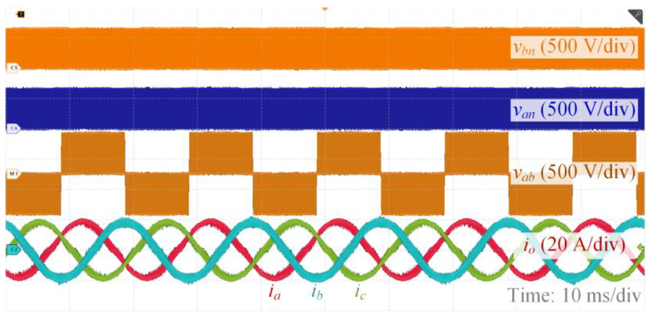
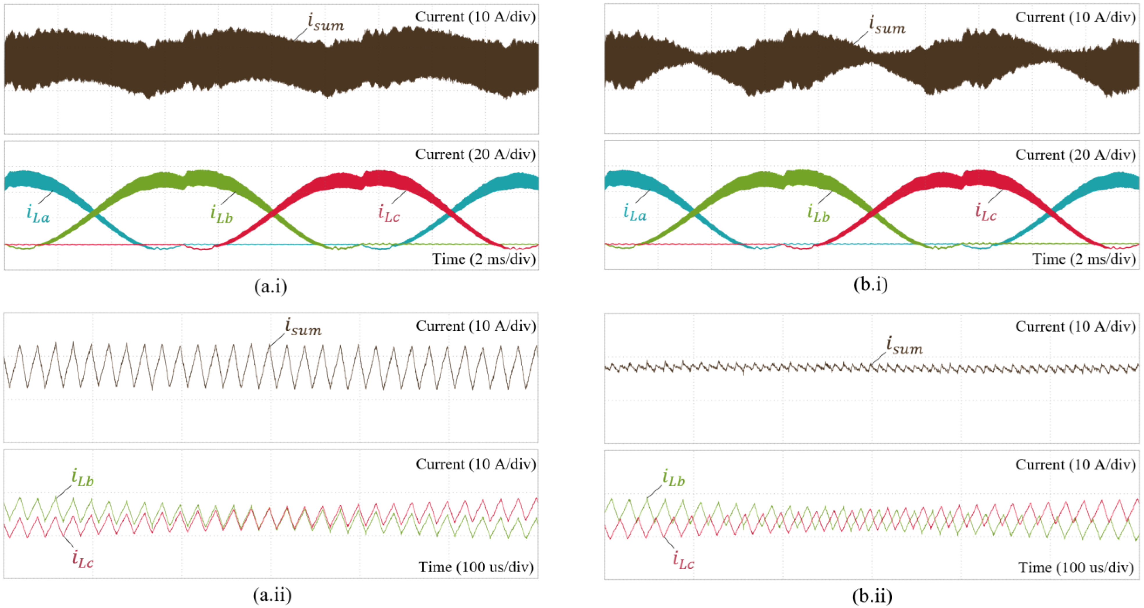
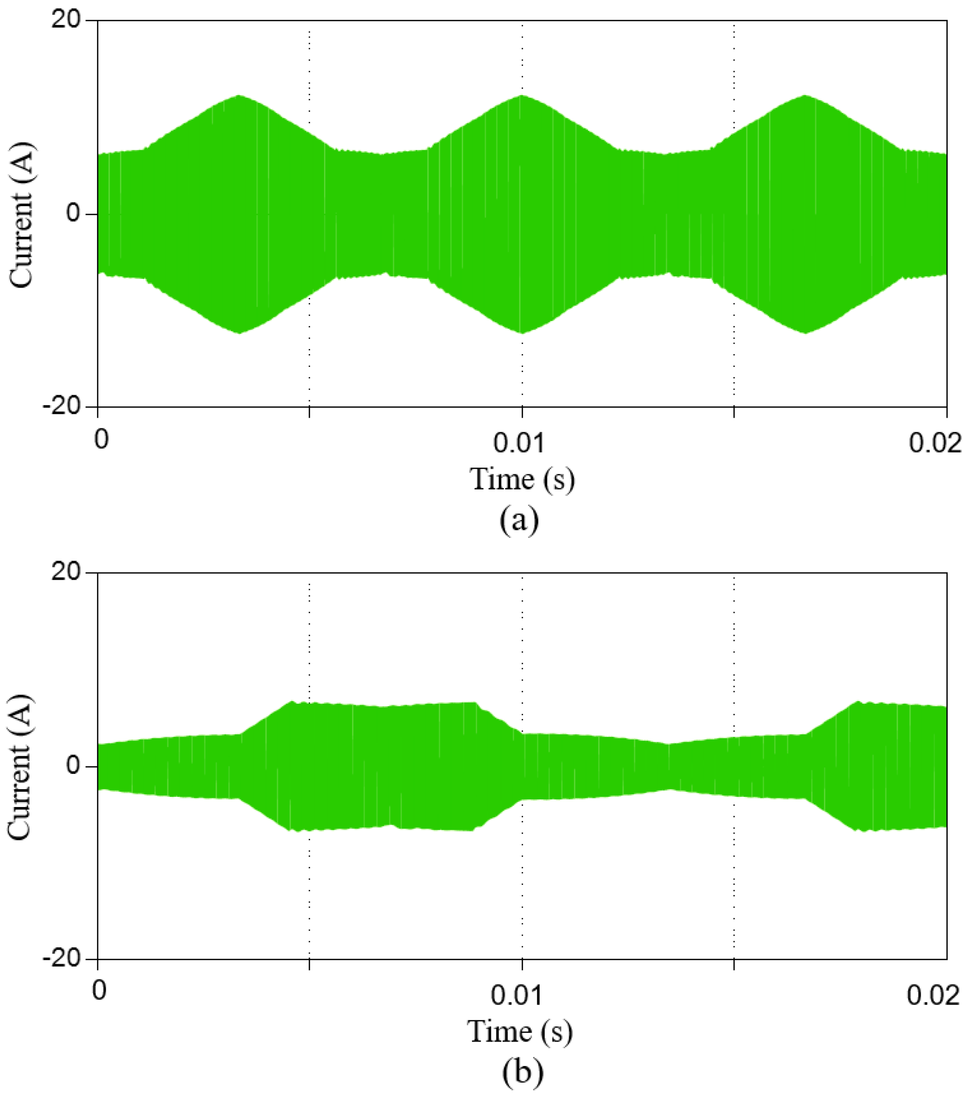
5. Experimental Results

A scaled-down hardware prototype is designed based on SiC MOSFETs, with a nominal power of 10 kW. SiC devices have been adopted in commercial EV traction inverters. SiC MOSFETs with parameters of 1200 V/40 mΩ are used in the prototype to represent the state-of-the-art technology. The performance of the BBI is validated with the prototype, and it is compared with the B-VSI topology with the same parameters and operating conditions. The parameters of the hardware prototype are shown in Table 1.
Thanks to the modular structure of the BBI, the hardware design can be simplified. The same boost-buck converter module design is reused for the three phase modules. The same hardware can be easily reconfigured as a B-VSI with three paralleled switch legs as the boost stage. The load is configured as a three-phase series-connected resistor-inductor branch to mimic a motor. This does not affect the efficiency and THD performance evaluation of the inverter.
Figure 13 shows the waveforms of the output phase voltage, phase-to-phase voltage, and output currents of the BBI. The waveform of the output phase voltages, referenced to the negative dc bus, conforms with the analysis in Section 2. When the reference voltage is higher than the input voltage, the phase module generates a smooth voltage waveform filtered by the dc bus capacitor. When the reference voltage is lower than the input voltage, the phase module generates a pulse-width-modulated voltage waveform with a magnitude equal to the input voltage. The phase-to-phase voltage is smooth during most of the fundamental cycle and only presents a ripple with a magnitude equal to the input voltage when any of the phase modules operates in buck mode.
Figure 14 shows the waveforms of the output phase voltage, phase-to-phase voltage, and output currents of the B-VSI employing SVPWM. The switch legs are constantly switching during the fundamental cycle. The phase-to-phase voltage is rich in high-frequency harmonics.
The harmonic content of the output current is then evaluated. The current waveform data measured by high-bandwidth current probes are computed in MATLAB to obtain the THDi value. The sampling frequency is 10 MHz and the maximum frequency for THDi calculation is 1 MHz. The THDi value with the BBI topology is 1.74%. It is slightly higher than the analytically calculated value due to nonideal factors in the hardware such as dead band time in the gate drive signals and device voltage drop. The THDi value with the BBI topology is 12.52%. It is much higher than the analytically calculated value mostly due to the high-frequency harmonics induced by the switching transients. As predicted by the theoretical analysis, the THDi with the BBI is much lower than that with the B-VSI. The low THDi with the BBI is mainly due to the inherent filtering effect of the dc-link capacitors even with drastically reduced switching actions.
As the switches of the B-VSI are constantly switched at a higher voltage and with high frequency, the efficiency of the B-VSI is relatively low. It is measured to be 96.8% at 10 kW. The total losses are calculated to be 322 W. For the BBI, the switch legs are clamped for 1/3 of a fundamental cycle where they generate no switching losses. When they are switching, they switch at the lower capacitor voltage of the phase modules. Therefore, the BBI has a higher efficiency. It is measured to be 97.7% at 10 kW, 0.9% higher than that of the B-VSI. The total loss is calculated to be 230 W, 28% lower than that of the B-VSI.
Figure 15 shows the measured data of the CM voltage and current of the two topologies. The experimental result matches with the analysis and simulation result. The RMS of the CM current with the BBI is 86 mA while it is 776 mA (9 times higher) with the B-VSI. This is also due to the inherent filtering effect, lower switched voltage, and much lower number of switching actions of the BBI.
The comparison of performance of the BBI and B-VSI is shown in Table 2. It is validated that the BBI topology has a higher efficiency, drastically lower THDi, and lower CM current.
Figure 16 shows the effect of the phase swapping interleaving method for the BBI. The interleaved phases are phases A and B during θ ( 0 , 2 π 3 ] , phases B and C during θ ( 2 π 3 , 4 π 3 ] , and phases C and A during θ ( 4 π 3 , 2 π ] . It is seen from the zoomed-in waveforms that the ripple currents of the interleaved phases have similar peak-to-peak values and opposite phases, so the ripple of the sum of the three input inductor currents is significantly reduced. The RMS ripple of the input current is reduced from 3.3 A to 2.4 A.

6. Conclusions

A comprehensive analysis of the CM voltage and current, and the THD of the output current is presented for the modular three-phase BBI. Analytical expressions are derived for the THD and the reduction ratio of the CM current compared to the conventional topology. A phase swapping interleaving method is designed to reduce the ripple of the input current.
The theoretical analyses are verified by extensive simulation and experimental results. It is validated that the BBI, compared to the conventional B-VSI, has a higher efficiency, much lower THDi, lower CM current, and lower voltage stress on the switch devices. The reduction in THDi and CM current compared to the conventional topology is more significant in the high-modulation-index range. The analysis and comparative evaluation prove that the BBI is a promising topology for the EV traction inverter.
The BBI has a higher component count compared to the conventional topology. However, the input stages are paralleled, and the full power is spread in the three phase modules. For the B-VSI, although there is only one switch leg for the booster stage, it usually also adopts semiconductor paralleling either at the chip level or at the device level. With a modular structure of the BBI, the same design can be used for the three phase modules so that the engineering effort can also be reduced.

Author Contributions

Conceptualization, D.W; methodology, Y.H. and Y.Z.; validation, Y.H.; formal analysis, Y.H.; writing—original draft preparation, Y.H.; writing—review and editing, D.W.; visualization, Y.H.; supervision, Y.Z. All authors have read and agreed to the published version of the manuscript.

Funding

This research received no external funding.

Institutional Review Board Statement

Not applicable.

Informed Consent Statement

Not applicable.

Data Availability Statement

The data presented in this study are available upon request from the corresponding authors.

Conflicts of Interest

The authors declare no conflict of interest.

References

  1. Lai, J.-S.; Nelson, D. Energy management power converters in hybrid electric and fuel cell vehicles. Proc. IEEE 2007, 95, 766–777. [Google Scholar] [CrossRef]
  2. Estima, J.; Cardoso, A.M. Efficiency analysis of drive train topologies applied to electric/hybrid vehicles. IEEE Trans. Veh. Technol. 2012, 61, 1021–1031. [Google Scholar] [CrossRef]
  3. Burress, T.; Campbell, S. Benchmarking EV and HEV power electronics and electric machines. In Proceedings of the 2013 IEEE Transportation Electrification Conference and Expo (ITEC), Detroit, MI, USA, 16–19 June 2013; pp. 1–6. [Google Scholar]
  4. Anwar, M.; Alam, M.K.; Gleason, S.E.; Setting, J. Traction Power Inverter Design for EV and HEV Applications at General Motors: A Review. In Proceedings of the 2019 IEEE Energy Conversion Congress and Exposition (ECCE), Baltimore, MD, USA, 29 September–3 October 2019; pp. 6346–6351. [Google Scholar]
  5. Chen, L.; Ge, B. High Power Traction Inverter Design and Comparison for Electric Vehicles. In Proceedings of the 2018 IEEE Transportation Electrification Conference and Expo (ITEC), Long Beach, CA, USA, 13–15 June 2018; pp. 583–588. [Google Scholar]
  6. Goli, C.S.; Essakiappan, S.; Sahu, P.; Manjrekar, M.; Shah, N. Review of Recent Trends in Design of Traction Inverters for Electric Vehicle Applications. In Proceedings of the 2021 IEEE 12th International Symposium on Power Electronics for Distributed Generation Systems (PEDG), Virtual, 28 June–1 July 2021; pp. 1–6. [Google Scholar]
  7. Shen, Z.J.; Omura, I. Power Semiconductor Devices for Hybrid, Electric, and Fuel Cell Vehicles. Proc. IEEE 2007, 95, 778–789. [Google Scholar] [CrossRef]
  8. Graovac, D.; Christmann, A.; Münzer, M. Power semiconductor solutions for hybrid-electric and electric vehicles. In Proceedings of the 2012 15th International Power Electronics and Motion Control Conference (EPE/PEMC), Novi Sad, Serbia, 4–6 September 2012; pp. LS4d.3-1–LS4d.3-8. [Google Scholar]
  9. Song, C.-H.; Song, I.-S.; Shin, H.-S.; Lee, C.-H.; Kim, K.-C. A Design of IPMSM for High-Power Electric Vehicles with Wide-Field-Weakening Control Region. IEEE Trans. Magn. 2022, 58, 1–5. [Google Scholar] [CrossRef]
  10. Chen, S.; Ding, S.; Shen, S.; Dai, Y.; Yang, Z.; Zhang, J. Influence of Field Weakening Control on Electromagnetic Force and Electromagnetic Vibration of SPMSMs. In Proceedings of the 2021 IEEE 12th Energy Conversion Congress & Exposition—Asia (ECCE-Asia), Singapore, 24–27 May 2021; pp. 221–225. [Google Scholar]
  11. Wang, B.; Zhang, J.; Yu, Y.; Zhang, X.; Xu, D. Unified Complex Vector Field-Weakening Control for Induction Motor High-Speed Drives. IEEE Trans. Power Electron. 2020, 36, 7000–7011. [Google Scholar] [CrossRef]
  12. Muta, K.; Yamazaki, M.; Tokieda, J. Development of New-Generation Hybrid System THS II—Drastic Improvement of Power Performance and Fuel Economy. In Proceedings of the SAE 2004 World Congress & Exhibition, Detroit, MI, USA, 8–11 March 2004. [Google Scholar]
  13. Burress, T.A.; Campbell, S.L.; Coomer, C.; Ayers, C.W.; A Wereszczak, A.; Cunningham, J.P.; Lin, H.T. Evaluation of the 2010 Toyota Prius Hybrid Synergy Drive System; Oak Ridge National Lab: Oak Ridge, TN, USA, 2011. [Google Scholar]
  14. Gebregergis, A.; Chowdhury, M.; Islam, M.; Sebastian, T. Modeling of permanent-magnet synchronous machine including torque ripple effects. IEEE Trans. Ind. Appl. 2015, 51, 232–239. [Google Scholar] [CrossRef]
  15. Mattavelli, P.; Tubiana, L.; Zigliotto, M. Torque-ripple reduction in pm synchronous motor drives using repetitive current control. IEEE Trans. Power Electron. 2005, 20, 1423–1431. [Google Scholar] [CrossRef]
  16. Feng, G.; Lai, C.; Kar, N.C. Practical Testing Solutions to Optimal Stator Harmonic Current Design for PMSM Torque Ripple Minimization Using Speed Harmonics. IEEE Trans. Power Electron. 2017, 33, 5181–5191. [Google Scholar] [CrossRef]
  17. Casadei, D.; Serra, G.; Tani, A.; Zarri, L. Theoretical and experimental analysis for the RMS current ripple minimization in induction motor drives controlled by SVM technique. IEEE Trans. Ind. Electron. 2004, 51, 1056–1065. [Google Scholar] [CrossRef]
  18. Kumar, A.C.B.; Narayanan, G. Variable-Switching Frequency PWM Technique for Induction Motor Drive to Spread Acoustic Noise Spectrum with Reduced Current Ripple. IEEE Trans. Ind. Appl. 2016, 52, 3927–3938. [Google Scholar] [CrossRef]
  19. Chen, C.; Wang, Y. Analysis of the impact of current ripple on the eddy current loss of axial-flux permanent magnet motor. In Proceedings of the 2014 IEEE Conference and Expo Transportation Electrification Asia-Pacific (ITEC Asia-Pacific), Beijing, China, 31 August–3 September 2014; pp. 1–5. [Google Scholar]
  20. Jeong, T.C.; Kim, W.H.; Kim, M.J.; Lee, K.D.; Lee, J.J.; Han, J.H.; Sung, T.-H.; Kim, H.-J.; Lee, J. Current Harmonics Loss Analysis of 150-kW Traction Interior Permanent Magnet Synchronous Motor through Co-Analysis of d-q Axis Current Control and Finite Element Method. IEEE Trans. Magn. 2013, 49, 2343–2346. [Google Scholar] [CrossRef]
  21. Yoshida, Y.; Nakamura, K.; Ichinokura, O. Calculation of eddy current loss in permanent magnet motor caused by carrier harmonics based on reluctance network analysis. In Proceedings of the 2013 15th European Conference on Power Electronics and Applications (EPE), Lille, France, 2–6 September 2013; pp. 1–6. [Google Scholar]
  22. Yamazaki, K.; Abe, A. Loss Investigation of Interior Permanent-Magnet Motors Considering Carrier Harmonics and Magnet Eddy Currents. IEEE Trans. Ind. Appl. 2009, 45, 659–665. [Google Scholar] [CrossRef]
  23. Van Do, T.; Trovao, J.P.F.; Li, K.; Boulon, L. Wide-Bandgap Power Semiconductors for Electric Vehicle Systems: Challenges and Trends. IEEE Veh. Technol. Mag. 2021, 16, 89–98. [Google Scholar] [CrossRef]
  24. Adabi, J.; Zare, F.; Ledwich, G.; Ghosh, A. Leakage current and common mode voltage issues in modern AC drive systems. In Proceedings of the 2007 Australasian Universities Power Engineering Conference, Perth, WA, Australia, 9–12 December 2007; pp. 1–6. [Google Scholar]
  25. Ogasawara, S.; Akagi, H. Modeling and damping of high-frequency leakage currents in PWM inverter-fed AC motor drive systems. IEEE Trans. Ind. Appl. 1996, 32, 1105–1114. [Google Scholar] [CrossRef] [Green Version]
  26. Murai, Y.; Kubota, T.; Kawase, Y. Leakage current reduction for a high-frequency carrier inverter feeding an induction motor. IEEE Trans. Ind. Appl. 1992, 28, 858–863. [Google Scholar] [CrossRef]
  27. Muetze, A.; Binder, A. Calculation of circulating bearing currents in machines of inverter-based drive systems. IEEE Trans. Ind. Electron. 2007, 54, 932–938. [Google Scholar] [CrossRef]
  28. Sundaresan, A.; Chandorkar, M. Traction Motor Bearing Failures Due to Bearing Currents in Electric Locomotives. In Proceedings of the 2019 IEEE Transportation Electrification Conference and Expo (ITEC), Novi, MI, USA, 19–21 June 2019; pp. 1–6. [Google Scholar]
  29. Kriese, M.; Wittek, E.; Gattermann, S.; Tischmacher, H.; Poll, G.; Ponick, B. Influence of bearing currents on the bearing lifetime for converter driven machines. In Proceedings of the 2012 XXth International Conference on Electrical Machines, Marseille, France, 2–5 September 2012; pp. 1735–1739. [Google Scholar] [CrossRef]
  30. Han, Y.; Wu, Z.; Wu, D. Analysis and Design of a Modular Three-Phase Boost-Buck EV Traction Inverter. In Proceedings of the 34th International Electric Vehicle Symposium and Exhibition (EVS34), Nanjing, China, 25–28 June 2021. [Google Scholar]
Figure 1. Circuit topology of (a) B-VSI: voltage source inverter with a preceding booster stage and (b) BBI: boost-buck inverter.
Wevj 13 00114 g001
Figure 2. The two modes of a phase module of the BBI: (a) boost mode and (b) buck mode.
Wevj 13 00114 g002
Figure 3. The characteristic waveforms of phase module A of the boost-buck inverter. (a) The input voltage Vin, reference output voltage van, (b) duty cycle d1 for the boost switch leg, duty cycle d2 for the buck switch leg, (c) input current iLa, and average output current ia are shown.
Wevj 13 00114 g003
Figure 4. The characteristic waveforms of three-phase output voltages and the CM voltage.
Wevj 13 00114 g004
Figure 5. The characteristic waveforms of (a) the module output voltage van, load neutral voltage von, (b) the phase voltage vao, and (c) current ia of the load.
Wevj 13 00114 g005
Figure 6. Simulated output voltage and current waveforms of the (a) BBI and (b) B-VSI. (a.i,b.i) Phase voltages, (a.ii,b.ii) phase-to-phase voltages, and (a.iii,b.iii) output currents.
Wevj 13 00114 g006
Figure 7. Simulated ripple characteristics of the output current of the (a) BBI and (b) B-VSI. (a.i,b.i) Ripple component of the output current and (a.ii,b.ii) instantaneous (green) and averaged (red) waveform of the output current.
Wevj 13 00114 g007
Figure 8. THD of the output current of the two topologies at different overall modulation indexes.
Wevj 13 00114 g008
Figure 9. Simulated output CM voltage and current of the (a) BBI and (b) B-VSI. (a.i,b.i) Instantaneous (green) and averaged (red) waveform of the CM voltage and (a.ii,b.ii) CM current.
Wevj 13 00114 g009
Figure 10. Zoomed-in detail of the CM voltage and current waveforms. (a) BBI and (b) B-VSI. (a.i,b.i) CM voltage and (a.ii,b.ii) CM current.
Wevj 13 00114 g010
Figure 11. Simulated waveforms of the ripple of the three summed input inductor currents (a) without and (b) with the phase swapping interleaving method.
Wevj 13 00114 g011
Figure 12. Voltage across the switch devices in a phase module. (a) BBI and (b) B-VSI.
Wevj 13 00114 g012
Figure 13. Experimental waveforms of the output phase voltages (van and vbn), phase-to-phase voltage vab, and three-phase currents (ia, ib, and ic) of the BBI.
Wevj 13 00114 g013
Figure 14. Experimental waveforms of the output phase voltages (van and vbn), phase-to-phase voltage vab, and three-phase currents (ia, ib, and ic) of the B-VSI.
Wevj 13 00114 g014
Figure 15. Measured waveforms of the CM voltage and current of (a) BBI and (b) B-VSI. (a.i,b.i) Waveform over a fundamental cycle. (a.ii,b.ii) Zoomed-in detail of the waveforms.
Wevj 13 00114 g015
Figure 16. Measured waveforms of the input inductor currents (iLa, iLb, iLc, isum = iLa + iLb + iLc) of the BBI. (a) Without interleaving. (b) With interleaving. (a.i,b.i) Waveforms over a fundamental cycle. (a.ii,b.ii) Zoomed-in detail of the waveforms.
Wevj 13 00114 g016
Table 1. Parameters of the prototype inverter.
ParameterValue
Nominal power (kW)10
Input DC voltage (V)200
Output voltage, L-L RMS (V)400
Input filter inductance (uH)240
DC bus Capacitance (uF)12
Switching frequency (kHz)50
Load inductance (mH)0.5
Table 2. Performance Comparison of the Two Topologies at Rated Condition.
TopologyEfficiencyTHDiCM Current RMS
BBI97.7%1.74%86 mA
B-VSI96.8%12.52%776 mA
Publisher’s Note: MDPI stays neutral with regard to jurisdictional claims in published maps and institutional affiliations.

