Article

An Inductor-Based and Capacitor-Free Bipolar Pulse Converter with Overvoltage Protection

Department of Illuminating Engineering and Light Sources, Institute for Electric Light Sources, School of Information Science and Engineering, Fudan University, 220 Handan Road, Shanghai 200433, China
*
Author to whom correspondence should be addressed.
World Electr. Veh. J. 2022, 13(5), 91; https://doi.org/10.3390/wevj13050091
Submission received: 25 March 2022 / Revised: 14 May 2022 / Accepted: 16 May 2022 / Published: 18 May 2022
(This article belongs to the Special Issue Modern Charging Techniques for Electrical Vehicles)

Abstract

:
The inductor-based and capacitor-free bipolar pulse converter can be applied to electric vehicle charging and realize an efficient and reliable charging-control strategy. Inductor-based converters can avoid the converter failure caused by the failure of energy storage capacitors and improve the reliability. An overvoltage protection scheme based on active clamping topology is used to protect this converter when the load impedance is too large. This overvoltage protection can take effect in an extremely short time (~50 ns) with little energy wasted. Furthermore, mathematical analyses of the proposed topology are presented and simulations based on LTspice are made, showing the feasibility and reliability of this circuit. Moreover, calculation of the power loss on MOSFETs is presented. A 201 W prototype converter with an efficiency of 83% is presented, and experimental results show that the converter can work reliably. This manuscript also proves the feasibility and application prospect of using this current-source-based converter for EV charging.

1. Introduction

The bipolar pulse converter has been widely applied in biotechnology, industrial applications, automotive applications, etc. [1,2]. In surgical practice, the bipolar pulse converter is one of the most commonly used electrosurgical generators (ESGs) [3]. When the high-frequency (~500 kHz) bipolar pulse is applied to a patient, joule heating can be induced in the target tissues and cells, which can be used to cut or weld tissues. As a result, surgery becomes much easier and more efficient with ESGs [4]. Furthermore, in the electric vehicle charging technology, the converting process of a typical on-board EV charger is: (1) AC (electrical grid) to DC (DC bus); (2) DC (DC bus) to AC (isolating transformers); (3) AC (isolating transformers) to DC (batteries) [5]. However, in the last step of this process, when the batteries are charging by a DC voltage, some gas and impurities will be attached to the plates and the electrolyte will be polarized, which can extend the charging time and shorten the life of batteries [6]. Therefore, an additional converter is applied to modulate the DC voltage and realizes some better charging modes. Among these modes, Reflex charging mode is an effective way to shorten the charging time and extend the battery life [7,8,9]. This mode uses a bipolar pulse converter as the charging supply: the positive pulse can charge the battery quickly while the negative pulse of a large current can clear the gas and impurities on the plates and make the electrolyte depolarize. Compared to monopolar pulse charging mode, Reflex charging mode results in a lower temperature rise, thus has a higher reliability [10]. In this way, an efficient and reliable charging-control strategy can be designed based on Reflex charging mode.
Refs. [11,12] have proposed bipolar pulse converters to realize Reflex charging mode. These Reflex chargers can charge the battery with a high efficiency and extend the battery life. Ref. [13] have proposed a Reflex charger based on soft switching, which can decrease the switching loss and improve the charging efficiency further. These bipolar pulse converters are voltage-source-based and cannot avoid the use of electrolytic capacitors as energy storage elements. However, especially in biotechnology and automotive applications, reliability is one of the most important concerns and long lifetime is also required [14]. For example, the typical lifetime target of power electronic converters in automotive application is 15 years [15]. Ref. [16] points out that power electronic converters are one of the decisive factors for reliability and lifetime in renewables. Meanwhile, electrolytic capacitor is often the weakest component in a power electronic system, which accounts for 60% of the failures while inductive elements only account for 6% [17]. Refs. [18,19,20] point out that the MTBF (mean time between failure) of converters is usually determined by the MTBF of electrolytic capacitors. During the operation of converters, factors, such as the temperature rise, can make electrolyte volatilize or denature, thus making capacitors fail [21]. That is to say, the lifetime of electrolytic capacitor limits the reliability and lifetime of the whole system. Therefore, using an inductor-based converter is attractive for the high reliability required applications. Refs. [22,23] have proposed an inductor-based bipolar pulse converter and the control scheme as an ESG. The authors have developed a control scheme, peak current mode control (CPM), which regulates a fixed-frequency power converter by comparing a measured inductor current to a reference current. Ref. [24] have implemented this converter based on GaN devices and show better performance. Refs. [22,23] have proved this current-source-based converter can achieve output modes of constant power, constant current, and constant voltage. Therefore, this converter has a possibility of application in most AC/DC scenarios, including EV charging. Moreover, the resonant circuit is one of the core technologies of wireless power transfer (WPT) systems [25]. Ref [26] has proposed an automatic resonance tracking scheme based on this converter, which proves that this current-source-based converter is expected to be used for wireless charging.
However, the feasibility of using this converter in EV charging has not been studied. Moreover, Refs. [22,23] have only considered normal applications while ignoring high voltage protection. For EV charging, the battery impedance is affected by several battery conditions (state-of-charge, temperature, current rate, and previous history) [27]. All of these conditions can make the battery impedance too large. In this circuit, an overvoltage output will occur when the load impedance is too large. As a result, overvoltage protection is necessary for this current-source-based converter. Although the current-source-based source can achieve high MTBF under normal application, the lack of overvoltage protection prohibits the application. Furthermore, Refs. [22,23] have not considered the power efficiency. In this manuscript, we have given comprehensive analyses.
This manuscript analyzes the feasibility of using this circuit to realize Reflex charging mode and further extends the circuit operation range from normal operation to the overvoltage protection. With a comprehensive analysis, the manuscript derives the equation of the output voltage and explains why the overvoltage phenomena happen with large load impedance. Furthermore, the manuscript proposes the overvoltage operation mode and extends the operation mode. Moreover, this manuscript gives the calculation of the power loss on MOSFET.
The structure of this manuscript is as below. In Section 2, the circuit topology, control strategy, and overvoltage protection scheme are presented. In Section 3, simulations of the converter and overvoltage protection are presented, showing the feasibility and reliability of this circuit. In Section 4, the results of a prototype converter are presented, showing the production of the desired output characteristic. Moreover, a calculation of the power loss on MOSFETs is presented. Finally, in Section 5, the results of this paper are summarized.

2. Converter Circuit Topology and Overvoltage Protection

This section is to present the circuit topology and overvoltage protection scheme. Section 2.1 presents the circuit topology and analyzes the working process of the converter. Section 2.2 presents the overvoltage protection scheme and analyzes the working mechanism.

2.1. The Circuit Topology and Working Process

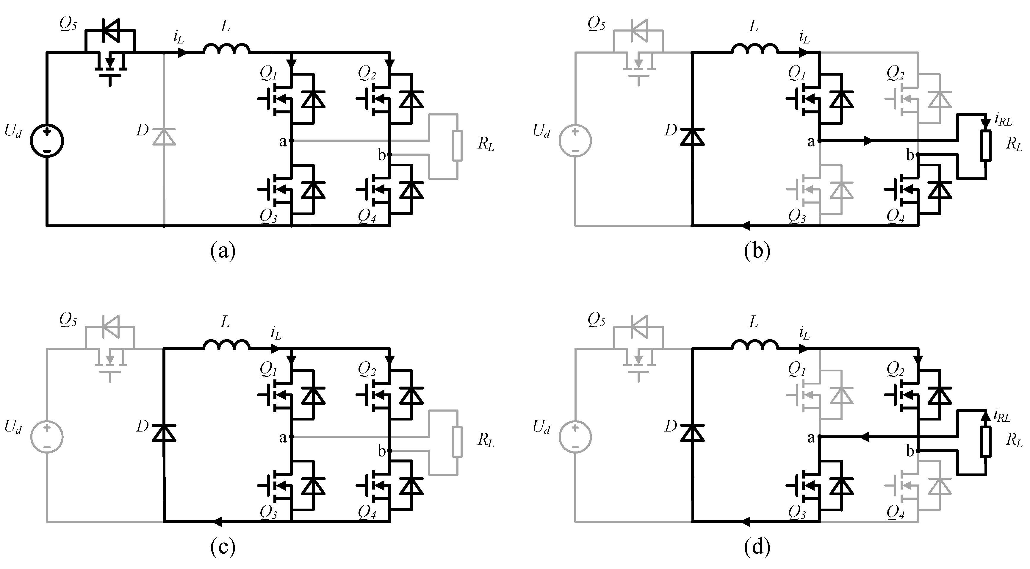
Figure 1 shows the proposed topology of the circuit, which contains a dc voltage supply Ud, a power inductor L, a freewheeling diode D and five semiconductor switches Q1~Q5. The output load is equivalent to a resistor RL.
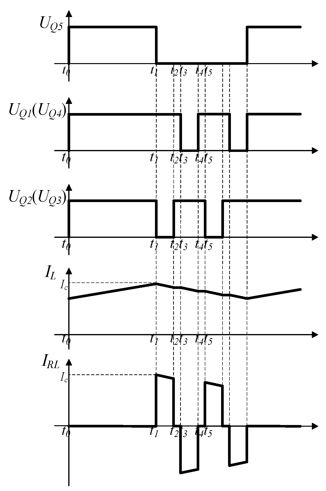
The balanced working process of this converter can be divided into two main stages: charging stage, in which the inductor L charged by source Ud, and discharging stage, in which the inductor L discharges to the load RL and generates bipolar pulses. The sequence diagram of the proposed converter and current passing through L and RL are shown in Figure 2. In order to simplify the diagram, only two pairs of bipolar pulses are shown in this figure. UQ1~UQ5 are the driving signals of switches Q1~Q5, respectively. Switch is ON when the driving signal is high. IL and IRL are the current passing through L and RL, respectively.
In order to analyze the converter operation and simplify the theoretical analysis, several assumptions are made as follows:
(1)
The switches are ideal MOSFETs except for the constant on-resistance.
(2)
The freewheeling diode is ideal except for the constant threshold voltage.
(3)
The power inductor is ideal except for the constant ESR.
The converter operation can be explained as follows:
(1)
Charging stage: (t0t1)
In this stage, all the MOSFETs are ON and the freewheeling diode D is OFF. The charging circuit of L is shown in Figure 3a. The freewheeling diode D is reverse biased. The potential of node a and node b are equal, so there is no current passing through RL.
Since all the MOSFETs are ON, the equivalent resistance of Q1~Q4 is RDS(on), where RDS(on) is the on-resistance of the MOSFETs. Therefore, the equivalent circuit resistance is R t o t a l = 2 R D S ( o n ) + R L ( E S R ) , where RL(ESR) is the ESR of L. The differential equation that describes the inductor current can be expressed as:
L d i L ( t ) d t + i L ( t ) R t o t a l = U d .
By solving this differential equation, the inductor current is:
i L ( t ) = I m ( 1 e 1 τ ) ,
where τ = L / R t o t a l is the time constant and I m = U d / R t o t a l is the static current.
As the inverse function, the charging time can be expressed as:
t ( i L ) = τ ln ( 1 i L I m ) .
Therefore, the duration of charging stage can be calculated as:
t c h a r g e = t ( i L t ) t ( i L 0 ) = τ ln I m i L t I m i L 0 ,
where iL0 is the initial current and iLt is the final current of the charging stage.
In order to make the peak current of L fixed when L begins to discharge, the charging time of L is controlled by the scheme CPM [23]. In this scheme, the inductor current iL(t) is compared with a reference current Ic. As the inductor current increases during the charging stage, switch Q5 will be turned off when iL(t) = Ic. In this way, the charging stage is over and the converter switches into discharging stage.
(2)
Discharging stage: (t1t5)
In this stage, switch Q5 is OFF and the freewheeling diode D is ON. Q1~Q4 form a full bridge. Power inductor L generates bipolar pulses on RL through the full bridge and D. In this case, the equivalent circuit resistance is R t o t a l = 2 R D S ( o n ) + R L ( E S R ) + R D + R L , where R D = V t h / i L is the equivalent on-state resistance of D and Vth is the threshold voltage. When R L 2 R D S ( o n ) + R L ( E S R ) + R D , Rtotal can be approximated to RL. The inductor current iL(t) is:
i L ( t ) = I c e R t o t a l L t ,
where deadtime is not included in t. In view of the fact that discharging time is short enough, this formula can be simplified to a linear process as:
i L ( t ) = I c ( 1 R t o t a l L t ) .
In discharging stage, the decrease in inductor current can be expressed as:
Δ i L = I c R t o t a l L t d i s c h a r g e ,
where tdischarge is the time of L discharging to RL.
As can be seen from this formula, when L is large enough or tdischarge is short enough, Δ i L I c . Therefore, this converter can be considered as a constant current source approximately.
The working process in discharging stage can be explained as follows:
(a)
Positive pulse: (t1t2)
The discharging circuit of L is shown in Figure 3b. At t1, Q2 and Q3 are turned off while Q1 and Q4 keep ON. The inductor current passes through RL from node a to node b, generating a positive pulse on RL. The load current iRL(t) is:
i R L ( t ) = i L ( t ) .
(b)
Deadtime: (t2t3) and (t4t5)
Because of the turn-on and turn-off delay of semiconductor switches, the bridge arms may be cut off at the same time and make the inductor open, which will produce a high voltage pulse and damage the components. Therefore, deadtime is set as a buffer state between positive and negative pulse. Different from capacitor-based converter, switches of the full bridge are all ON during deadtime in this inductor-based converter. The freewheeling current path for the inductor is shown in Figure 3c. The potential of node a and node b are equal, so there is no current passing through RL. Therefore, the consumption of energy stored by inductor can be ignored and inductor current remains constant approximately during deadtime.
(c)
Negative pulse: (t3t4)
The discharging circuit of L is shown in Figure 3d. At t1, Q1 and Q4 are turned off while Q2 and Q3 keep ON. The inductor current passes through RL from node b to node a, generating a negative pulse on RL. The load current iRL(t) is:
i R L ( t ) = i L ( t ) .
According to the working process and control strategy, the duty cycle d of this converter is unfixed. When the load impedance RL changes in the process of converter working, the duty cycle will change to obtain a constant inductor peak current. That is to say, the value of the duty cycle is adaptive in different working conditions, which is determined for each cycle individually [28,29].

2.2. Overvoltage Protection Scheme

For a constant voltage source, if the load impedance is too small, the circuit will be over current and damage the components as a result. However, because of the inductor-based topology, this converter will not be overcurrent in general. On the contrary, if the load impedance is too large when the inductor is discharging, there will be a high voltage across the load, which may make the semiconductor switches break down. For example, as is shown in Figure 3b, the voltage across the load is:
u R L ( t ) = i R L ( t ) R L = I c R L e R t o t a l L t .
Switch Q1 and Q4 are ON, so the voltage across their drain and source equals to Conduction Voltage Drop UDS(on), which is very small. However, switch Q2 and Q3 are OFF. Therefore, they are in parallel with a turn-on switch and the load. The drain-source voltages are:
u Q 2 ( t ) = u R L ( t ) + u Q 1 ( t ) = I c R L e R t o t a l L t + U D S ( o n ) ,
u Q 3 ( t ) = u R L ( t ) + u Q 4 ( t ) = I c R L e R t o t a l L t + U D S ( o n ) .
As can be seen from this formula, if RL is too large, there will be a high voltage across the turn-off switches. When uQ2(t) = uQ3(t) > UDSS(BR), Q2 and Q3 are very likely to be broken down, where UDSS(BR) is the drain-source breakdown voltage of the switch.
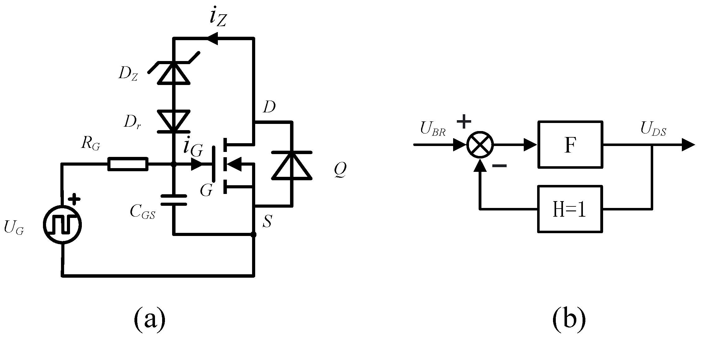
Therefore, in order to protect the circuit in case the load impedance is too large, an active clamped topology based on Transient Voltage Suppressors (TVS) is proposed [30]. The topology of this overvoltage protection scheme is shown in Figure 4a. The MOSFET Q in Figure 4a is the protected semiconductor switch and G, D, S are the gate, drain, source of Q, respectively. Source UG provides driving signals for Q. RG is the gate equivalent resistor and CGS is the equivalent stray capacitor between gate and source. A TVS DZ and a reverse series diode Dr are connected between drain and gate. Dr is used to prevent the case that the driving signal output by UG is coupled to drain and source.
As discussed before, Q may be broken down because of the overvoltage across drain and source when Q is OFF. However, because of the protection scheme, the drain-source voltage can be clamped to a save voltage when an overvoltage occurs. The working mechanism is as follows. When Q is OFF and the potential difference between drain and gate meets the condition:
U D G = U D S U G S U B R ,
where UDS is the drain-source voltage and UBR is the breakdown voltage of DZ, DZ will be broken down. As Q is OFF and the output of UG is low at this moment, UDG equals to UDS approximately. Therefore, a current iZ will flow into gate, which can increase the gate potential and provide a driving signal for Q. Additionally, then Q will turn on and draw some of the inductor current. Hence, the load current iRL(t) will decrease, which results in the decrease in uRL(t). According to Formulas (8) and (9), the drain-source voltage will decrease as well.
This process can be considered as negative feedback. The control loop model is shown in Figure 4b [30]. In this control model, the breakdown voltage UBR is the reference value and the drain-source voltage UDS is the controlled object. Module F is the forward transfer function, which can be considered as the effect of gate-source voltage UGS on iRL(t) and UDS. In this way, UDS will be rapidly stabilized and equal to UBR approximately, which realizes the active clamping process and overvoltage protection.
As can be seen, using the active clamped topology is an excellent way to realize overvoltage protection. First of all, because of the rapid response of TVS, the protection can take effect in a very short time. Second, TVS only provides a trigger signal to turn on the MOSFET, so the current passing through TVS is relatively small and only lasts for a short time, guaranteeing that the TVS will not be damaged because of overcurrent or overheat. Third, the voltage clamping is realized by drawing some of the inductor current into other pathways, which will return to the inductor finally. Therefore, the energy stored in the inductor will not be wasted.

3. Results Simulation of the Converter and Overvoltage Protection

This section is to verify the feasibility of the proposed topology in Figure 1 and Figure 4a. Section 3.1 presents the simulation of the converter and analyzes the output waveforms. Section 3.2 presents the simulation of the overvoltage protection. The simulations are made based on LTspice.

3.1. Simulation of the Converter

The related parameters in this simulation are listed in Table 1. We have performed the simulation using the actual physical model of all the circuit components.
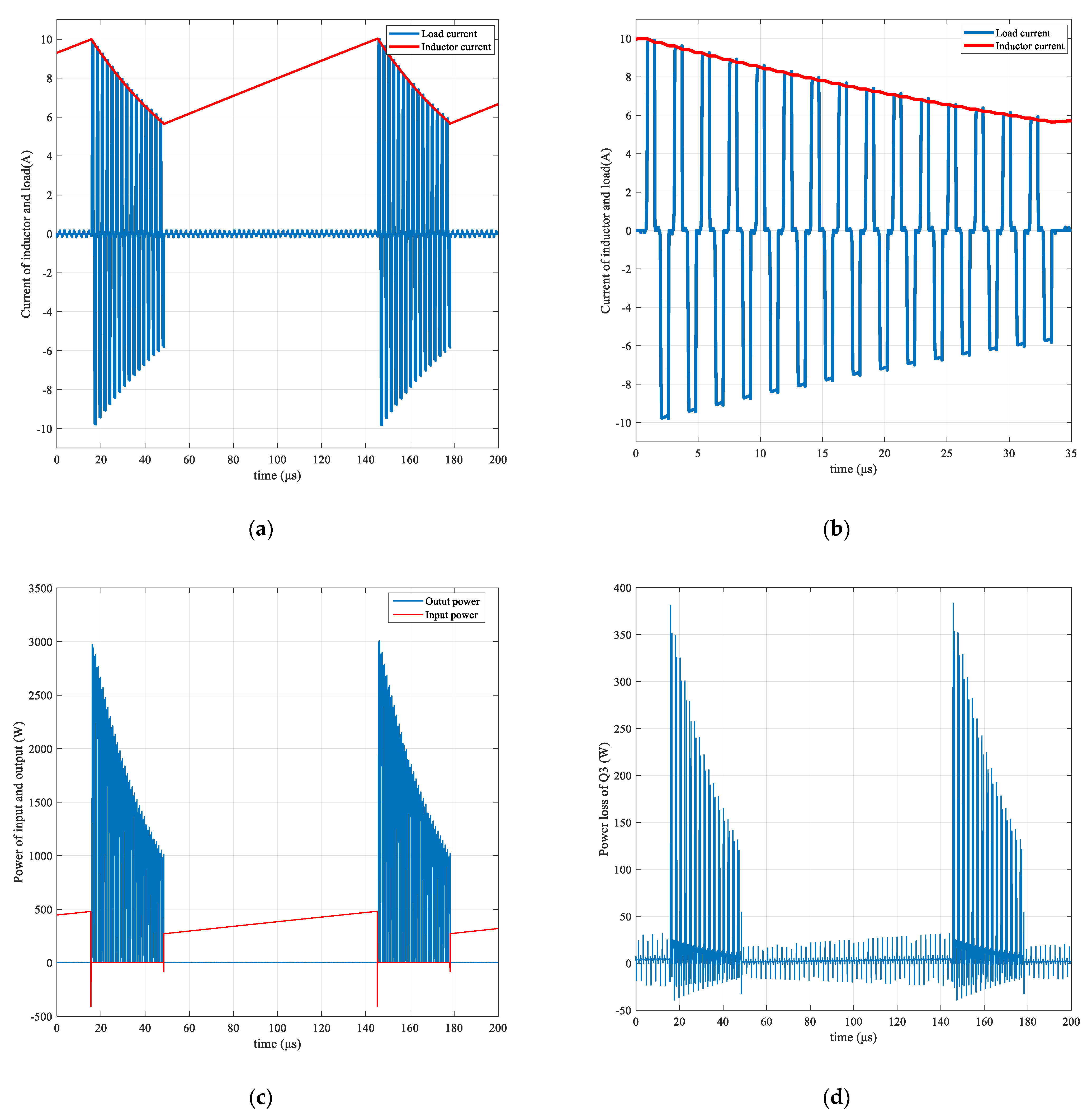
With the proposed circuit topology and control scheme, the simulation results are shown in Figure 5. As can be seen, in the charging stage, the inductor current iL increases linearly from 5.8 A to 10.0 A until iL = Ic and the load current iRL is zero. The duration of the charging stage in this simulation is about 96.8 μs. The on-resistance RDS(on) of the MOSFETs can be obtained from the physical model, which is 190 mΩ. Therefore, according to Formula (4), the charging time can be calculated as about 94.2 μs, which agrees well with the simulation results. In the discharging stage, iL almost decreases linearly and bipolar pulses are generated on the load. The amplitude of iRL equals to iL. The simulation results can prove that the theoretical analyses in Section 2 are accurate and reliable.
As is shown in Figure 5c, this converter can output a DC power to the resistor load. By averaging the instantaneous power in a single cycle in Figure 5c, the average input power is about 253 W and the average output power is about 221 W, with a power efficiency of about 87%. Similarly, the average power loss of MOSFET Q3 is about 6.08 W. However, for an EV charger, it can hardly output power to the battery indeed, because the power flows from the battery to the inductor in the negative pulse. In this case, define the output power in the negative pulse as a negative value. Then, the average output power is only about 5.37 W, which can hardly output power to the battery indeed. In order to provide a considerable power flow to the battery, the width of the positive pulse must be much longer than that of the negative pulse. In this way, a simulation of Reflex charging mode based on this converter is realized and shown in Appendix A.
According to the converter operation and the simulation results, this converter is not a DC/DC converter and will not produce any ripples in principle. Moreover, since the working process of this converter is based on the charging and discharging of the power inductor, the ripples of the input DC source will not be coupled to the output. Last but not least, this converter is controlled by peak current mode (CPM), so the ripple of the input DC source will not affect the output peak current either. As a verification, we have added a simulation in Appendix B, in which the input DC source has ripples.

3.2. Simulation of the Overvoltage Protection

The related parameters in this simulation are listed in Table 2. We have performed the simulation using the actual physical model of all the circuit components.
With the proposed circuit topology and control scheme, the simulation results are shown in Figure 6. When a current of 10 A passes through the load, the voltage across the load will be 600 V, which can break down the TVS and the overvoltage protection will take effect according to Section 2.2. As can be seen in Figure 6d, when the discharging stage starts, the TVS is broken down and a very small current iZ pass through TVS and provides a trigger signal to turn on Q3. Then, in Figure 6c Q3 draws a current of about 4.0 A, which will return to the inductor. As a result, there will be only a current of about 6.0 A passing through the load, clamping the load voltage to 360 V. The response time of this overvoltage protection is only about 44 ns and there is no overvoltage spike on the load. With the decrease in iL, it cannot produce an overvoltage across the load anymore, as is shown in Figure 6b. In this condition, the TVS will not be broken down and all of the inductor current will flow into the load. These results agree well with the theoretical analyses in Section 2.2. However, the clamping voltage is higher than UBR. This is because the TVS is not an ideal device and the voltage across TVS will not remain constant but increase slightly with the increase in breakdown current. As a result, when the negative feedback process in Figure 4b reaches a steady state, the clamping voltage will be a little higher than UBR.

4. Experiments and Results

This section is to verify the previous analysis and circuit operation. The inductor-based bipolar pulse converter in Figure 1 with the overvoltage protection in Figure 4a is assembled and experimental tests are conducted. Section 4.1 presents the output of the converter under normal conditions. Section 4.2 presents the output when overvoltage protection takes effect. Section 4.3 establishes a power loss model of the switches and calculates their power loss under this working condition.

4.1. Output under Normal Conditions

The prototype of the converter is shown in Figure 7. Electrical parameters of the converter and test conditions are listed in Table 3.
The output current of the converter is measured by a current probe (Pearson Current Monitor Model 4100, 1 V/A, rise time 10 ns). The current probe is connected to a digital oscilloscope (Rohde and Schwarz, bandwidth 1 GHz, sample rate 5 GSa/s).
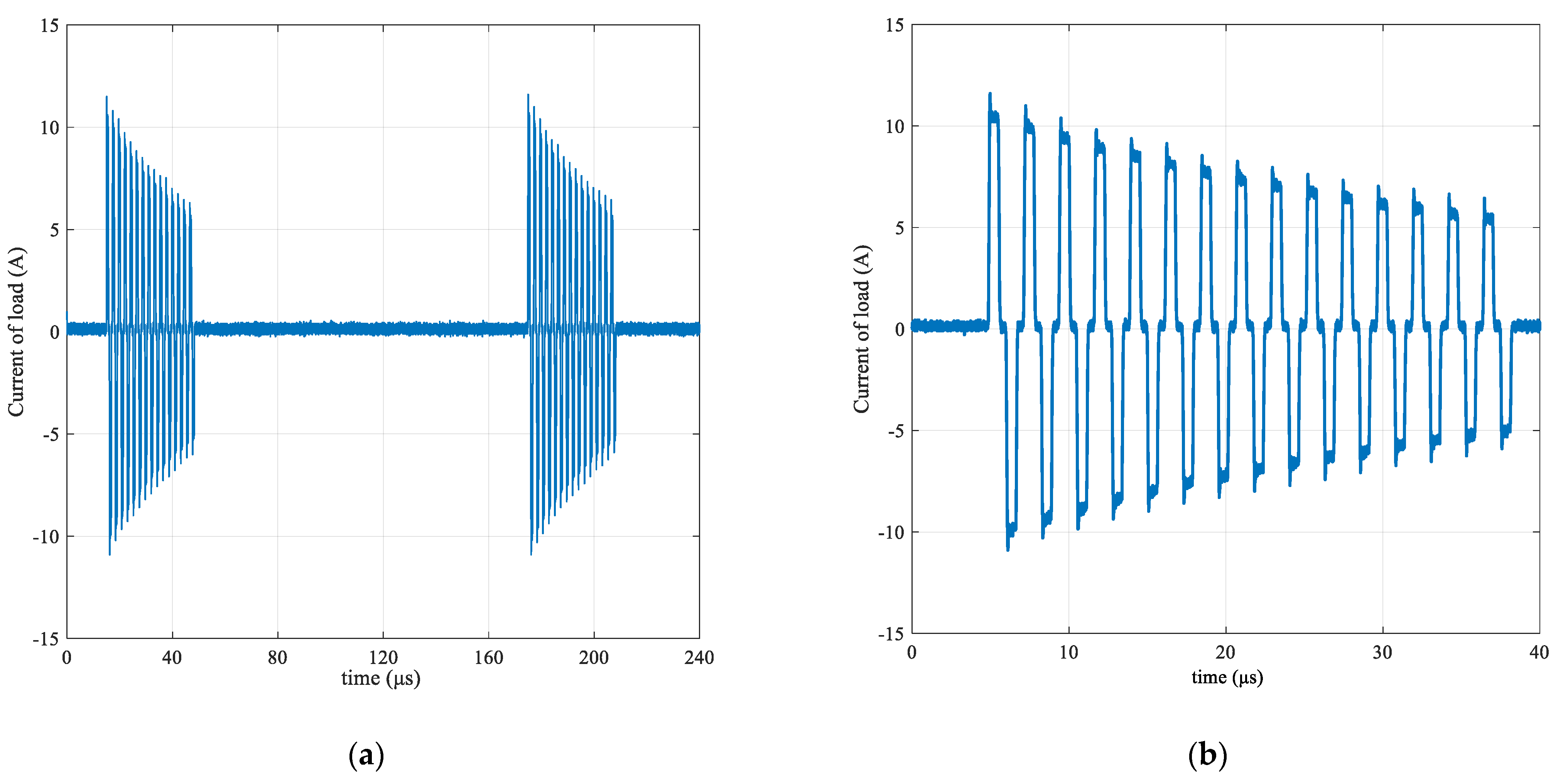
Figure 8 shows waveforms from the converter, delivering 10 A into a resistor of 30 Ω. As can be seen, in the charging stage, there is no current passing through the resistor. Additionally, in the discharging stage, the resistor obtains bipolar pulses with a peak current of 10 A, ignoring the spikes. By calculating the root mean square (RMS) of the current in Figure 8a, the average input power is about 242 W and the output power is about 201 W, with a power efficiency of about 83%. These results fit well with the simulation in Section 3.1.

4.2. Output When Overvoltage Protection Takes Effect

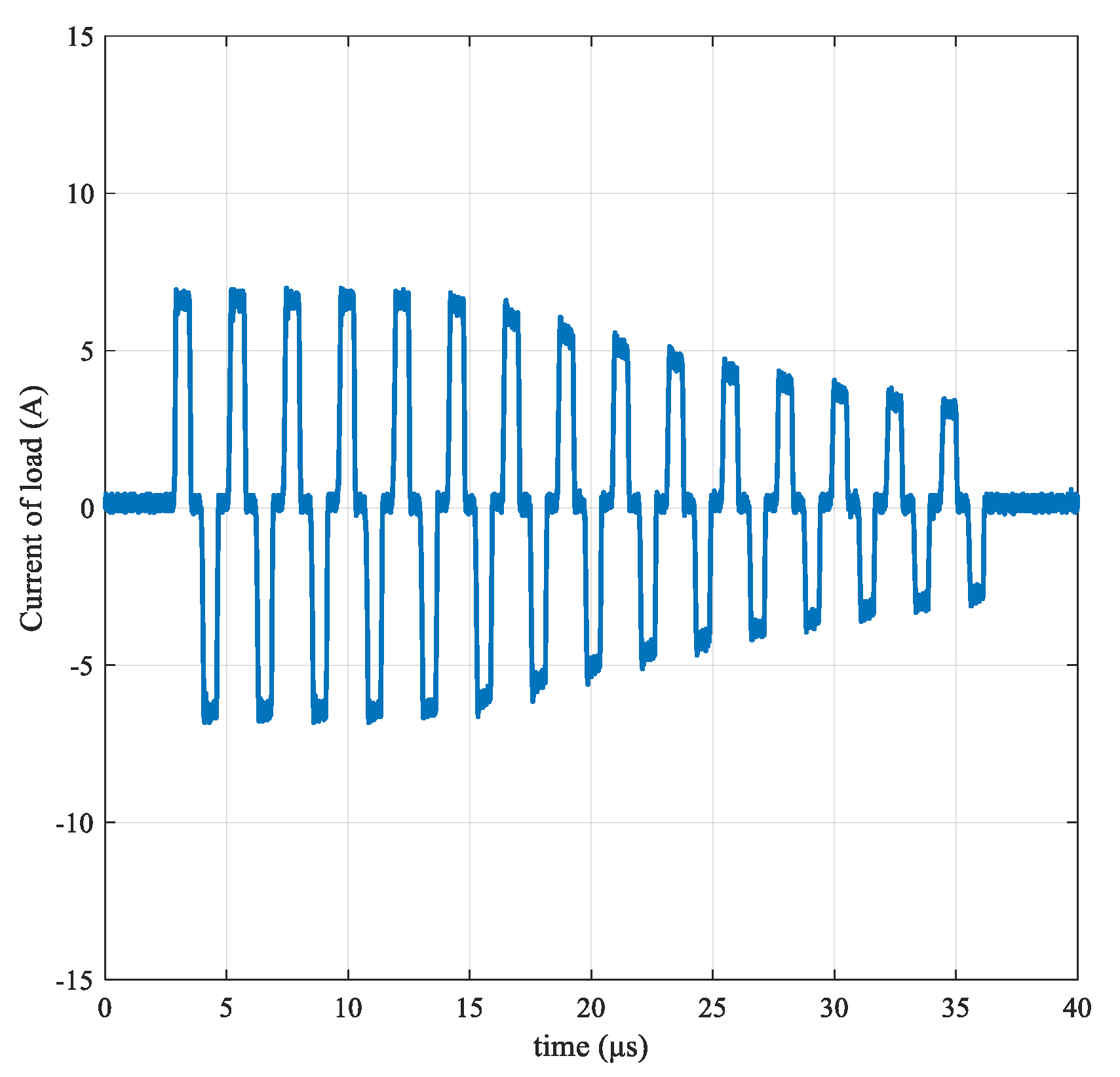
In order to test the overvoltage protection of the converter, a larger resistor of 60 Ω is used as the load. A current of 10 A will produce a voltage of 600 V across the resistor, which is higher than the breakdown voltage of the TVS. The waveforms from the converter in the condition of overvoltage protection are shown in Figure 9. In the first few pulses, there is a current of about 6.5 A passing through the load and the output voltage is clamped to about 390 V. The protection takes effect very quickly and there is no voltage spike on the load. With the decrease in inductor current, the output voltage is lower than the breakdown voltage of TVS UBR and overvoltage protection does not take effect anymore. The waveforms fit well with the theoretical analyses in Section 2.2 and the simulation in Section 3.2. However, the clamping voltage is about 390 V, which is even higher than that in the simulation. This is because the parasitic parameters of the practical circuit result in a longer feedback time.

4.3. Model and Calculation of the Power Loss on MOSFETs

Since the converter is working at a high frequency, the semiconductor switches Q1~Q4 are very likely to be overheated, which can damage them and limit the properties of the converter. The switching frequency of Q5 is much lower, so its power loss is much smaller. In order to improve the reliability of the converter, this section will establish a power loss model of the switches Q1~Q4 and calculate their power loss.

4.3.1. Switching Loss

Supposing that all of the switches are working normally, the working pattern of Q1~Q4 is the same in this converter. Take Q3 as an example. In one cycle, Q3 has two different working patterns. In the charging stage, Q3 keeps ON. Additionally, in the discharging stage, Q3 works at a high frequency. Therefore, the switching loss is mainly consumed in the discharging stage.
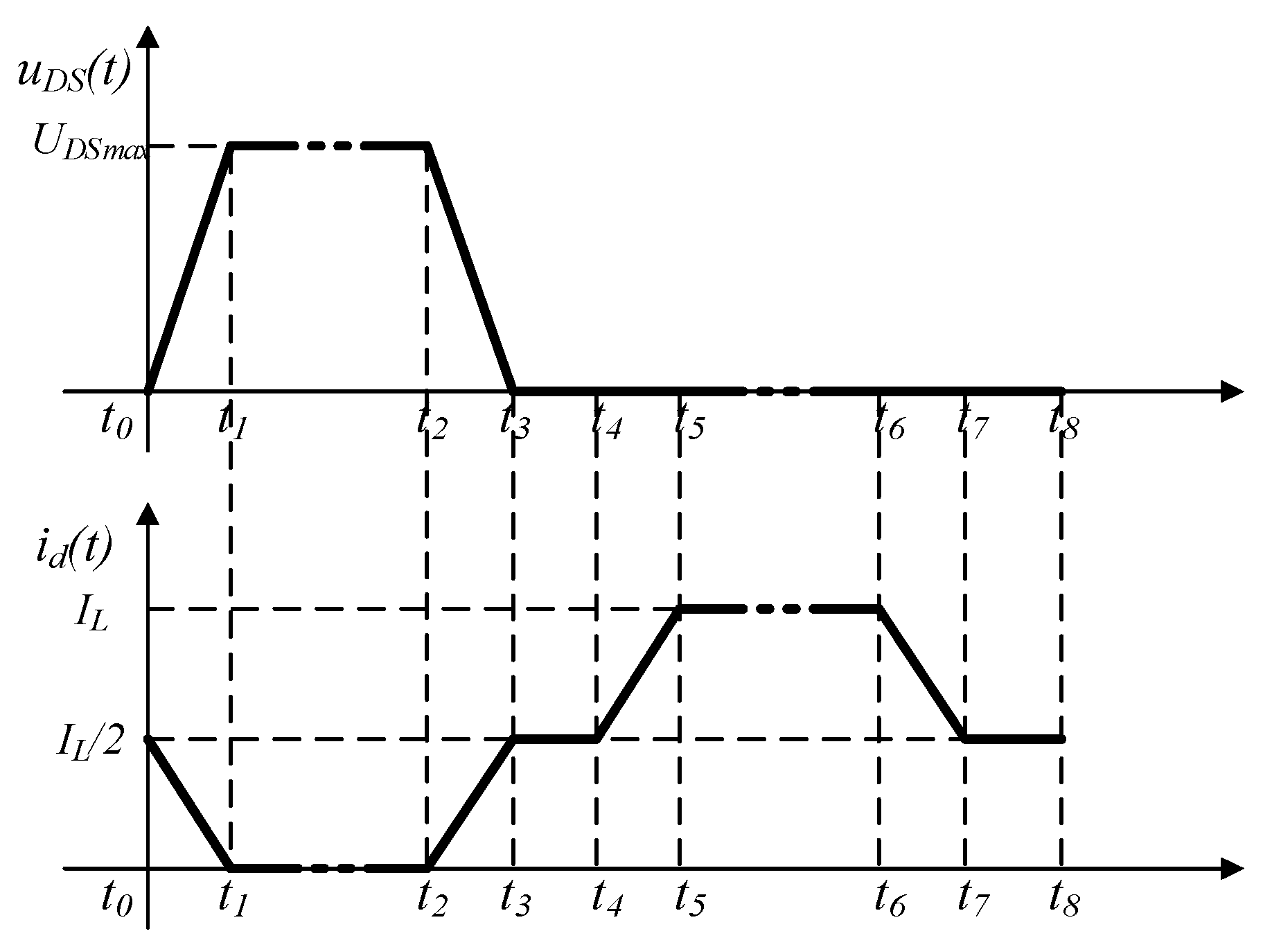
According to Ref. [31], during the turn-on transient and turn-off transient, there is a crossover period, in which the current Id and drain-source voltage UDS of Q3 are both nonzero. Switching loss is caused as a result. In order to simplify the calculation, suppose that Id and UDS vary linearly during the turn-on transient and turn-off transient. The waveform of Id and UDS in a bipolar pulse cycle is shown in Figure 10, including a positive pulse, a negative pulse and two deadtime periods.
In Figure 10, the peak drain-source voltage is
U D S m a x = I L R L ,
where IL is the inductor current.
In the deadtime period, Q1~Q4 are all ON. Therefore, it can be regarded that the inductor current will flow into the two bridge arms evenly. Consequently, Id in the deadtime period is
I d = 1 2 I L .
In a bipolar pulse cycle, the energy of switching loss can be calculated as
E s w = 0 t t u r n o n u D S ( t ) i d ( t ) d t + 0 t t u r n o f f u D S ( t ) i d ( t ) d t = 1 6 U D S m a x I d t c r o s s ,
where tcross = tturnon + tturnoff, tturnon, and tturnoff are the time of turn-on and turn-off process, respectively.
Suppose that there are n bipolar pulses in the discharging stage. Considering the decrease in inductor current in the discharging stage, the energy of switching loss in the discharging stage is less than nEsw. According to Formula (6), the inductor current can be considered as varying linearly, so the decrease in inductor current between two adjacent bipolar pulses can be calculated as
Δ I L = I c I L 0 n ,
where IL0 is the inductor current when the charging stage starts.
Combining Formula (14)–(17), the total energy of switching loss in discharging stage can be calculated as
E s w ( t o t a l ) = i = 0 n 1 1 12 ( I c i Δ I L ) 2 R L t c r o s s .

4.3.2. Conduction Loss

According to the working pattern, in the charging stage, Q3 is always ON. Additionally, in the discharging stage, Q3 is ON in the deadtime and negative pulse. Conduction loss is caused in these cases:
(1)
Charging stage
According to Formula (1), the inductor current in the charging stage can be expressed as:
i L ( t ) = I L 0 + d i L ( t ) d t t = I L 0 + U d L e t / τ t I L 0 + U d L t .
Since Q1~Q4 are all ON in the charging stage, it can be regarded that the inductor current will flow into the two bridge arms evenly. The current of Q3 is:
i d ( t ) = 1 2 i L ( t ) .
Combining Formulas (19) and (20), the energy of conduction loss in charging stage can be calculated as:
E c o n ( c h a r g e ) = 0 t c h a r g e i d 2 ( t ) R D S ( o n ) d t ,
where tcharge is the charging duration and tcharge can be calculated according to Formula (4). RDS(on) is the drain-source on-resistance of the MOSFET. According to Ref. [32], the on-resistance of the diode is mainly affected by the junction temperature, the variable of RDS(on) is ignorable when the heat dissipation is good.
(2)
Discharging stage
A bipolar pulse cycle includes two deadtime periods and Id in deadtime is expressed as Formula (15). Taking the decrease in inductor current in the discharging stage into consideration, the total energy of conduction loss in the deadtime can be calculated as:
E c o n ( d e a d t i m e ) = i = 0 n 1 2 ( I c i Δ I L 2 ) 2 R D S ( o n ) t d e a d ,
where tdead is the deadtime.
When the converter outputs negative pulses, Q1, Q4 are OFF and Q2, Q3 are ON. Therefore, the current of Q3 equals to inductor current. In this case, the energy of conduction loss can be calculated as:
E c o n ( p u l s e ) = i = 0 n 1 ( I c i Δ I L ) 2 R D S ( o n ) t p u l s e .
In conclusion, the average power loss of Q1~Q4 can be calculated as:
P l o s s = E s w ( t o t a l ) + E c o n ( d e a d t i m e ) + E c o n ( p u l s e ) T ,
where T = tcharge + n(2tpulse + 2tdead) is the time of a charging and discharging cycle.
Under the working condition in Section 4.1, the time of charging stage, turn-on process and turn-off process can be measured approximately according to Figure 8. Additionally, the drain-source on-resistance of the MOSFET can be found in the datasheet of SPP21N50C3. As a result, the power loss of each MOSFET (Q1~Q4) can be estimated according to the above formulas. The related electrical parameters and calculation results are listed in Table 4.
The result of power loss is slightly higher than that of the simulation in Section 3.1. Except for the error caused by measurement and the approximations of the theoretical analysis, the non-ideal driving signals and driving circuit in the practical converter result in a longer turn-on and turn-off time, thus a higher power loss.
According to the calculation results, the energy of conduction loss nearly accounts for half of the energy loss on MOSFETs, which is quite different from capacitor-based converters. As can be seen in the analysis of the conduction loss in this converter, in order to make the inductor current continuous, the MOSFETs are almost always ON when the converter is working, which causes a relatively high conduction loss. In contrast, in a capacitor-based converter with similar functions, the MOSFETs are ON only when they generates pulses [33]. Consequently, the inductor-based converter has high power loss and lower efficiency.

5. Conclusions

This research proposes an inductor-based and capacitor-free bipolar pulses converter with overvoltage protection. The proposed topology uses only power inductors as the energy storage elements instead of capacitors, and thus has better reliability and higher MTBF. The output peak current can be adjusted by changing the reference current with the control model CPM. A 201 W prototype converter with an efficiency of 83% is presented and discharge tests on resistors are performed in order to verify the feasibility and reliability of this proposed converter. The results show that this converter can generate bipolar pulses stably and proves the feasibility and application prospect of using this current-source-based converter for EV charging. When the load impedance is too large and causes overvoltage, the overvoltage protection module can rapidly take effect (~50 ns) and suppress the overvoltage spikes with preserving most of the inductor energy. This protection topology is expected to be used for open circuit protection of inductor or current source. This manuscript also proves that the inductor-based converter has higher power loss than that in a capacitor-based converter, decreasing the power efficiency. Moreover, since the energy storage density of capacitors is much higher than inductors, this inductor-based converter needs a larger size than a capacitor-based converter [34]. Therefore, taking all the concerns into consideration, the inductor-based converter would be attractive in applications with high-reliability and long-lifetime requirements while not sensitive to power loss and power density.

Author Contributions

Conceptualization, J.X., X.Y. and K.L.; data curation, J.X.; investigation, J.X. and X.Y.; methodology, J.X., X.Y. and H.Z.; supervision, H.Z., J.Q. and K.L.; validation, H.Z.; writing—original draft, J.X.; writing—review & editing, H.Z., J.Q. and K.L. All authors have read and agreed to the published version of the manuscript.

Funding

National Natural Science Foundation of China: 51877046; Pioneering Project of Academy for Engineering and Technology of Fudan University: gyy2018-002.

Conflicts of Interest

The authors declare no conflict of interest.

Appendix A

This section is to prove this converter can provide a considerable power flow to the battery. In this section, a simulation of Reflex charging mode based on this converter is realized. The width of the positive pulse is much longer than that of the negative pulse in this simulation. The simulation is made based on LTspice.
The related parameters in this simulation are listed in Table A1. In this simulation, we have performed the simulation using the actual physical model of all the circuit components.
Table A1. Related parameters in the simulation of the Reflex charging mode converter.
ParameterValue
Power inductorL = 1 mH, ESR = 50 mΩ
Input dc voltageUd = 48 V
Load impedanceRL = 30 Ω
Reference currentIc = 10 A
Positive pulse widthtp_pulse = 5000 ns
Negative pulse widthtn_pulse = 400 ns
deadtimetdead = 300 ns
Number of bipolar pulses in discharge stagen = 5
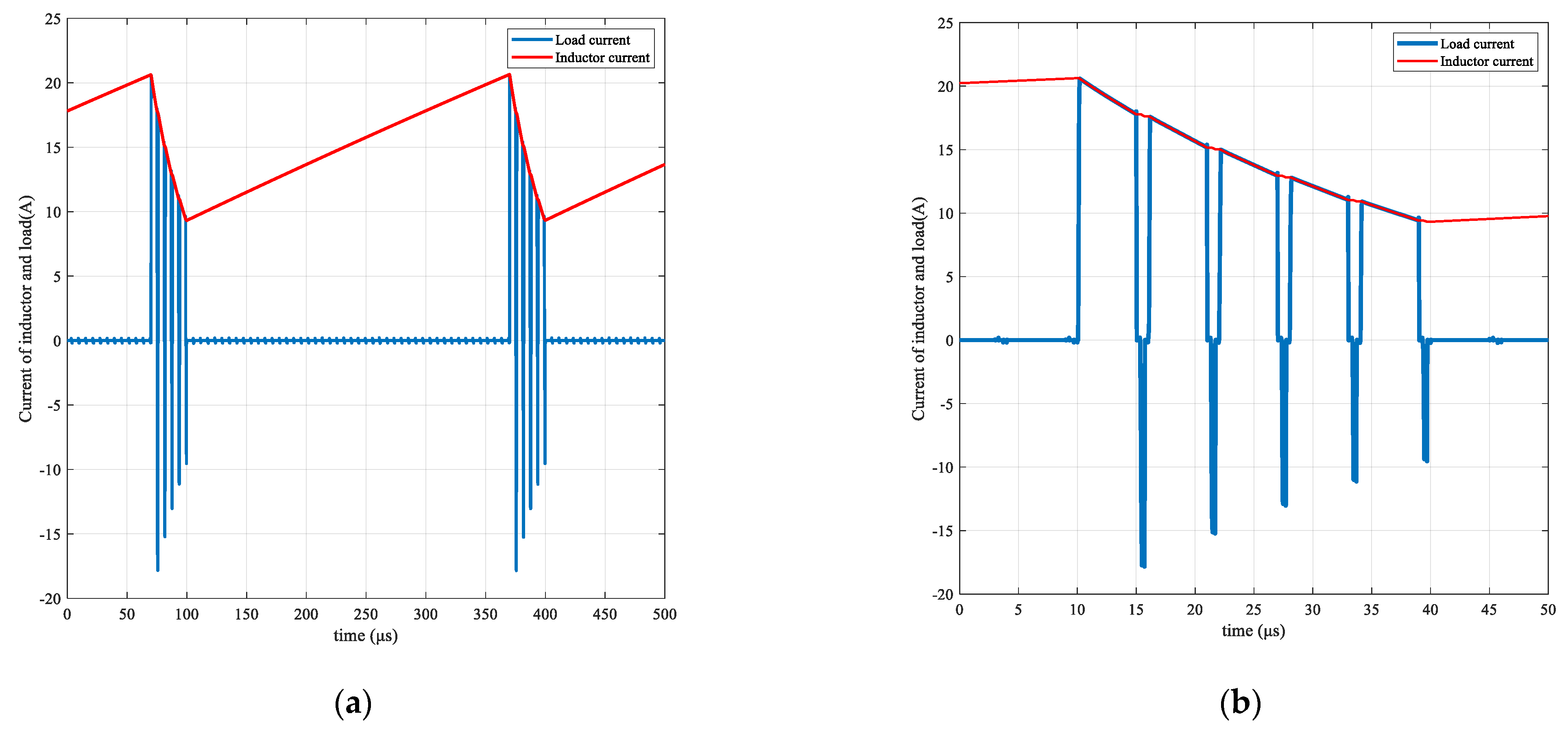
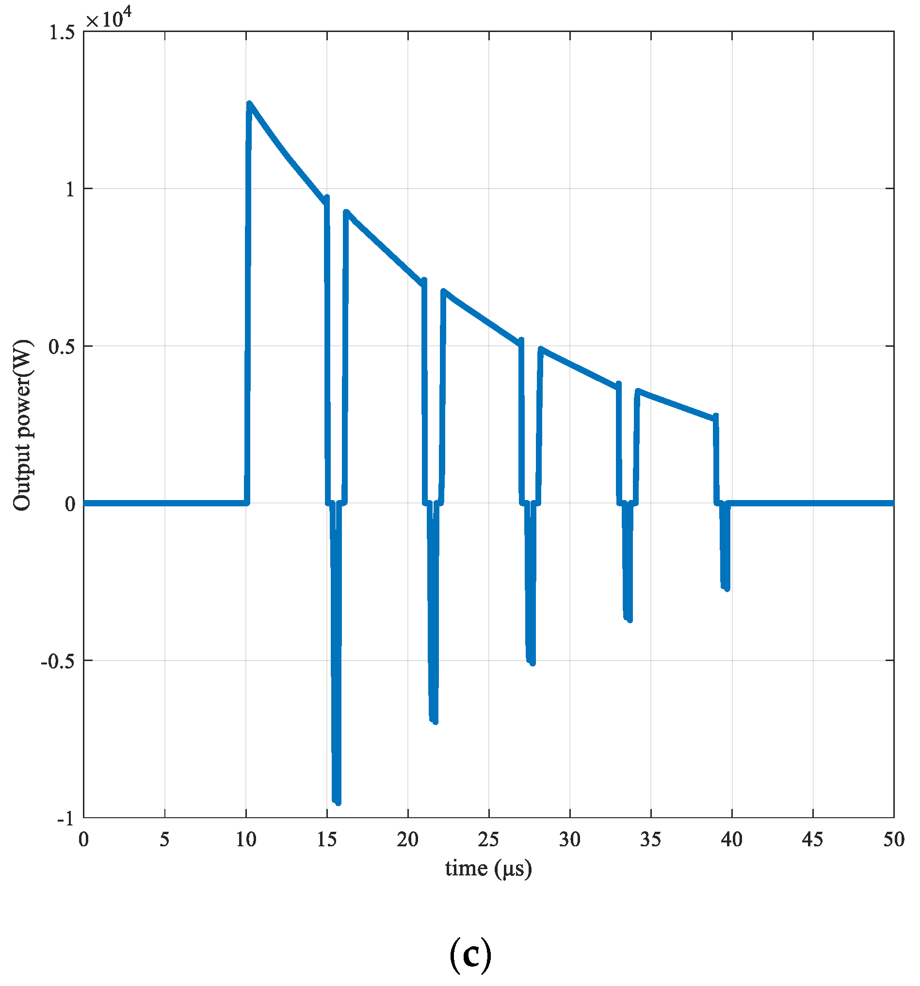
With the proposed circuit topology and control scheme, the simulation results are shown in Figure A1. As can be seen, the width of the positive pulse is much longer than that of the negative pulse. As defined in Section 3.1, the output power in the negative pulse is a negative value, which is shown in Figure A1c. In this case, the average output power is about 501 W, which can provide a considerable power flow to the battery.
Figure A1. Simulation results of the Reflex charging mode converter: (a) train of pulses; (b) zoomed-view of the pulses train; (c) output power on the load.
Wevj 13 00091 g0a1aWevj 13 00091 g0a1b

Appendix B

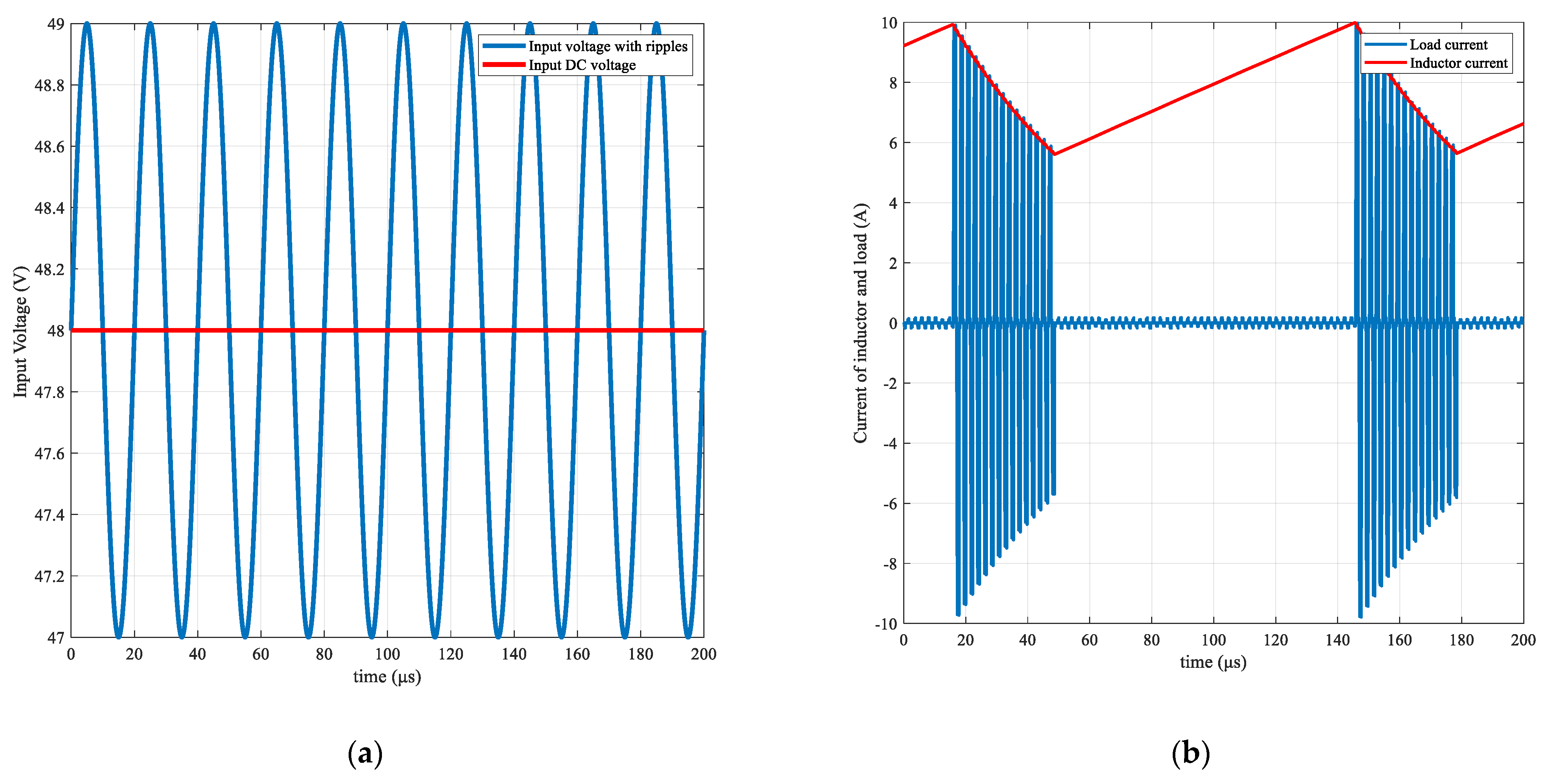
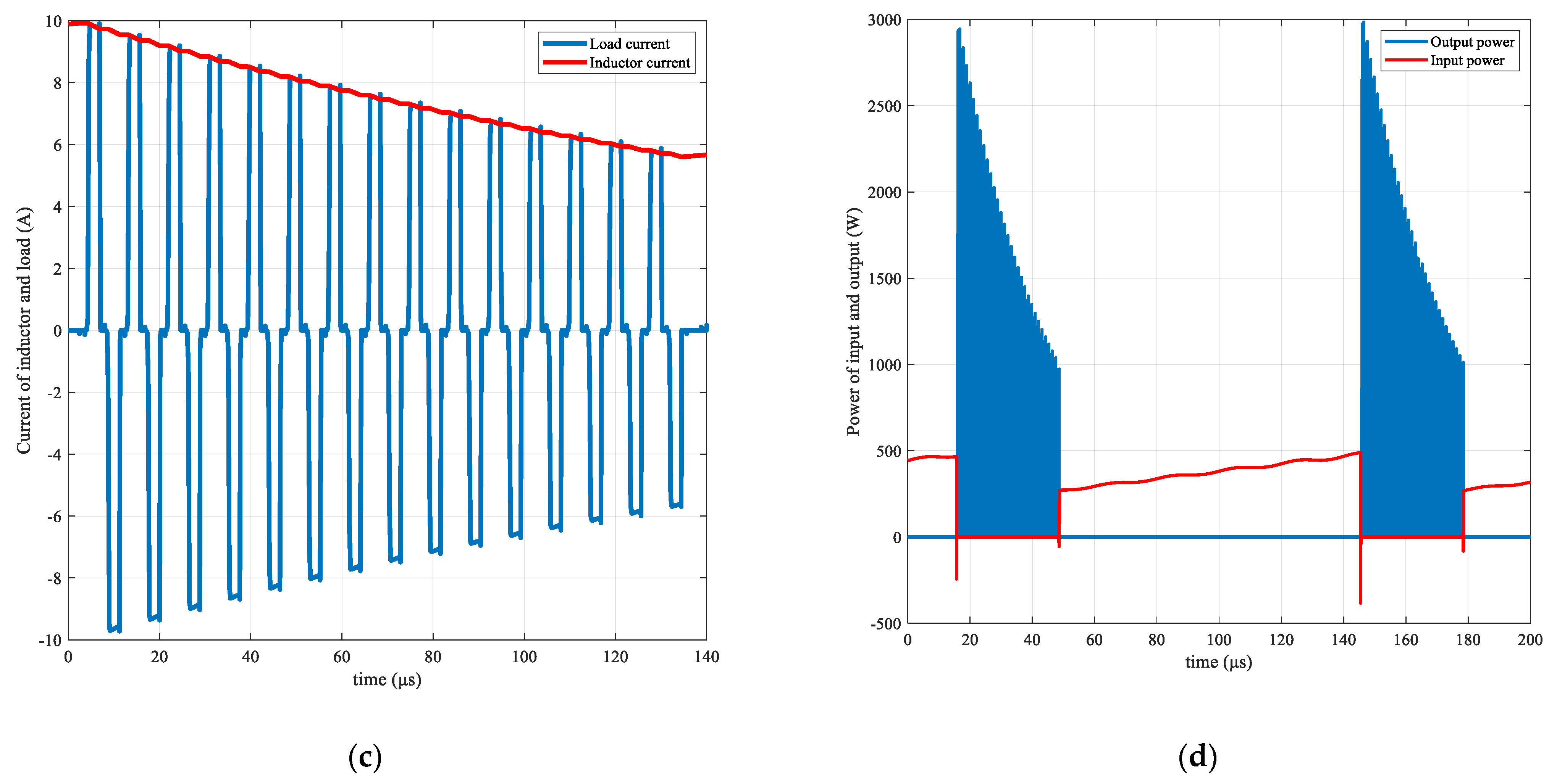
This section is to prove that the ripples of the input DC source will not be coupled to the output, and that the ripple of the input DC source will not affect the output peak current either. The simulation results are shown in Figure A2.
Figure A2. Simulation results of the converter: (a) input voltage with ripples; (b) train of pulses; (c) zoomed-view of the pulses train; (d) input power of the DC source and output power on the load.
Wevj 13 00091 g0a2aWevj 13 00091 g0a2b
As is shown in Figure A2a, we have added a sinusoid voltage (1 V, 50 kHz) as a ripple signal to the 48 V input DC source. As a result, the input voltage is ud(t) = Ud + sin2πft, where Ud = 48 V and f = 50 kHz. The output pulses are shown in Figure A2b,c, which is the same as that in the simulation in Section 3.1. The input and output power are shown in Figure A2d. As can be seen, the input power in the charging stage is not linear anymore because of the ripples. However, the inductor current is unaffected and the ripples of the input DC source are not coupled to the output.

References

  1. Akiyama, H.; Sakugawa, T.; Namihira, T.; Takaki, K.; Minamitani, Y.; Shimomura, N. Industrial Applications of Pulsed Power Technology. IEEE Trans. Dielectr. Electr. Insul. 2007, 14, 1051–1064. [Google Scholar] [CrossRef] [Green Version]
  2. Mankowski, J.; Kristiansen, M. A review of short pulse generator technology. IEEE Trans. Plasma Ence 2002, 28, 102–108. [Google Scholar] [CrossRef]
  3. Curtiss, L.E. High frequency currents in endoscopy: A review of principles and precautions. Gastrointest. Endosc. 1973, 20, 9–12. [Google Scholar] [CrossRef]
  4. Morris, M.L.; Tucker, R.D.; Baron, T.H.; Song, L.M.W.K. Electrosurgery in gastrointestinal endoscopy: Principles to practice. Am. J. Gastroenterol. 2009, 104, 1563–1574. [Google Scholar] [CrossRef] [PubMed]
  5. Sujitha, N.; Krithiga, S. RES based EV battery charging system: A review. Renew. Sustain. Energy Rev. 2017, 75, 978–988. [Google Scholar] [CrossRef]
  6. Huet, F. A review of impedance measurements for determination of the state-of-charge or state-of-health of secondary batteries. J. Power Sources 2012, 70, 59–69. [Google Scholar] [CrossRef]
  7. Guo, Y.; Zhang, C. Study on the fast charging method of lead-acid battery with negative pulse discharge. In Proceedings of the 4th International Conference on Power Electronics Systems and Applications, Hongkong, China, 8–10 June 2011. [Google Scholar]
  8. Marcos, J.; Dios, J.; Cao, A.M.; Doval, J.; Poza, F. Fast lead-acid battery charge strategy. In Proceedings of the Twenty-First Annual IEEE Applied Power Electronics Conference and Exposition, 2006, Beijing, China, 15–19 May 2006. [Google Scholar]
  9. Hua, C.C.; Lin, M.Y. A study of charging control of lead-acid battery for electric vehicles. In Proceedings of the 2000 IEEE International Symposium on Industrial Electronics, Cholula, Mexico, 4–8 December 2000. [Google Scholar]
  10. Pagar, O.; Darekar, M.; Gawde, S.; Bhartiy, J.; Deshmukh, B. Comparative Evaluation of Fast Charging Systems for the Advanced Electric Vehicles with Pulse Charging & Reflex Charging. In Proceedings of the International Conference on IoT Based Control Networks & Intelligent Systems—ICICNIS 2021, Kottayam, India, 28–29 June 2021. [Google Scholar]
  11. Lai, C.-M.; Teh, J.; Cheng, Y.-H.; Li, Y.-H. A reflex-charging based bidirectional DC charger for light electric vehicle and DC-microgrids. In Proceedings of the TENCON 2017–2017 IEEE Region 10 Conference, Penang, Malaysia, 5–8 November 2017; pp. 280–284. [Google Scholar]
  12. Vignan, M.; Hemarani, P. Implementation of Variable Duty Ratio Reflex Charging of Li-ion Batteries. In Proceedings of the 2021 IEEE International Power and Renewable Energy Conference (IPRECON), Kollam, India, 24–26 September 2021; pp. 1–5. [Google Scholar]
  13. Ahmadi, F.; Adib, E.; Azari, M. Soft Switching Bidirectional Converter for Reflex Charger With Minimum Switches. IEEE Trans. Ind. Electron. 2020, 67, 8355–8362. [Google Scholar] [CrossRef]
  14. Kumar, G.K.; Elangovan, D. Review on fault-diagnosis and fault-tolerance for DC–DC converters. IET Power Electron. 2020, 13, 1–13. [Google Scholar] [CrossRef]
  15. Wang, H.; Liserre, M.; Blaabjerg, F.; Peter, D.; Jacobsen, J.B.; Kvisgaard, T.; Landkildehus, J. Transitioning to Physics-of-Failure as a Reliability Driver in Power Electronics. IEEE J. Emerg. Sel. Top. Power Electron. 2014, 2, 97–114. [Google Scholar] [CrossRef]
  16. Yang, Y.; Wang, H.; Sangwongwanich, A.; Blaabjerg, F. Design for Reliability of Power Electronic Systems. In Power Electronic Handbook, 4th ed.; Butterworth-Heinemann: Oxford, UK, 2018; pp. 1423–1440. [Google Scholar]
  17. Pang, H.M.; Bryan, P. A life prediction scheme for electrolytic capacitors in power converters without current sensor. In Proceedings of the Applied Power Electronics Conference & Exposition, Palm Springs, CA, USA, 21–25 February 2010. [Google Scholar]
  18. Hao, M.; Wang, L. Fault diagnosis and failure prediction of aluminum electrolytic capacitors in power electronic converters. In Proceedings of the Conference of IEEE Industrial Electronics Society, Raleigh, NC, USA, 6–10 November 2005. [Google Scholar]
  19. Kulkarni, C.; Biswas, G.; Koutsoukos, X.; Goebel, K.; Ce Laya, J. Physics of Failure Models for Capacitor Degradation in DC-DC Converters. In Proceedings of the The Maintenance and Reliability Conference, San Antonio, TX, USA, 25–28 May 2010. [Google Scholar]
  20. Adler, P.; Mallwitz, R. Time-based Reliability Analysis of Electrolytic Capacitors for Automotive Applications Using Multi-Domain Simulation. In Proceedings of the 2021 22nd International Conference on Thermal, Mechanical and Multi-Physics Simulation and Experiments in Microelectronics and Microsystems (EuroSimE), St. Julian, Malta, 19–21 April 2021; pp. 1–6. [Google Scholar]
  21. Gasperi, M.L. Life prediction model for aluminum electrolytic capacitors. In Proceedings of the IAS Meeting, San Diego, CA, USA, 6–10 October 1996. [Google Scholar]
  22. Friedrichs, D.A.; Erickson, R.W.; Gilbert, J. A new system architecture improves output power regulation in electrosurgical generators. Annu. Int. Conf. IEEE Eng. Med. Biol. Soc. 2011, 2011, 6870–6873. [Google Scholar] [CrossRef] [PubMed]
  23. Friedrichs, D.A.; Erickson, R.W.; Gilbert, J. A new dual current-mode controller improves power regulation in electrosurgical generators. IEEE Trans. Biomed. Circuits Syst. 2012, 6, 39–44. [Google Scholar] [CrossRef] [PubMed]
  24. Sarnago, H.; Lucia, O.; Burdío, J. High performance boost inverter featuring GaN-based devices for electro surgical units. In Proceedings of the Applied Power Electronics Conference & Exposition, Tampa, FL, USA, 26–30 March 2017. [Google Scholar]
  25. Jiang, C.; Chau, K.T.; Liu, C.; Lee, C.H.T. An Overview of Resonant Circuits for Wireless Power Transfer. Energies 2017, 10, 894. [Google Scholar] [CrossRef]
  26. Liu, X.; Colli-Menchi, A.; Gilbert, J.; Friedrichs, D.A.; Malang, K.; Sanchez-Sinencio, E. An Automatic Resonance Tracking Scheme With Maximum Power Transfer for Piezoelectric Transducers. IEEE Trans. Ind. Electron. 2015, 62, 7136–7145. [Google Scholar] [CrossRef]
  27. Wang, X.; Wei, X.; Zhu, J.; Dai, H.; Zheng, Y.; Xu, X.; Chen, Q. A review of modeling, acquisition, and application of lithium-ion battery impedance for onboard battery management. ETransportation 2021, 7, 100093. [Google Scholar] [CrossRef]
  28. Middlebrook, R.D. Modeling Current-Programmed Buck and Boost Regulators. IEEE Trans. Power Electron. 1989, 4, 36–52. [Google Scholar] [CrossRef] [Green Version]
  29. Tan, F.D.; Middlebrook, R.D. A Unified Model for Current-Programmed Converters. IEEE Trans. Power Electron. 1995, 10, 397–408. [Google Scholar] [CrossRef] [Green Version]
  30. Zhang, C.; Liang-Deng, H.U. Research of Active Clamping Circuit for Medium-high Voltage High Power IGBT Driver. Power Electron. 2017, 51, 5. [Google Scholar]
  31. Xiong, Y.; Sun, S.; Jia, H.; Shea, P.; Shen, Z.J. New Physical Insights on Power MOSFET Switching Losses. IEEE Trans. Power Electron. 2009, 24, 525–531. [Google Scholar] [CrossRef]
  32. Acquaviva, A.; Rodionov, A.; Kersten, A.; Thiringer, T.; Liu, Y. Analytical conduction loss calculation of a mosfet three-phase inverter accounting for the reverse conduction and the blanking time. IEEE Trans. Ind. Electron. 2020, 68, 6682–6691. [Google Scholar] [CrossRef]
  33. Yao, C.; Dong, S.; Zhao, Y.; Zhou, Y.; Mi, Y.; Li, C. High-frequency composite pulse generator based on full-bridge inverter and soft switching for biological applications. IEEE Trans. Dielectr. Electr. Insul. 2016, 23, 2730–2737. [Google Scholar] [CrossRef]
  34. Seeman, M.D.; Ng, V.W.; Le, H.-P.; John, M.; Alon, E.; Sanders, S.R. A comparative analysis of Switched-Capacitor and inductor-based DC-DC conversion technologies. In Proceedings of the 2010 IEEE 12th Workshop on Control and Modeling for Power Electronics (COMPEL), Boulder, CO, USA, 28–30 June 2010; pp. 1–7. [Google Scholar]
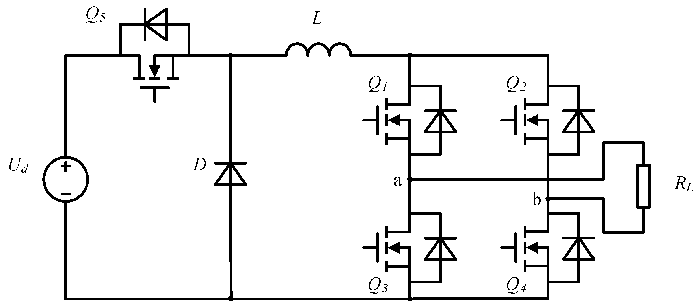
Figure 1. Topology of the converter.
Wevj 13 00091 g001
Figure 2. Sequence diagram of the proposed converter.
Wevj 13 00091 g002
Figure 3. Simplified circuit of the converter in different stages: (a) charging stage; (b) positive pulse; (c) deadtime; (d) negative pulse.
Wevj 13 00091 g003
Figure 4. The overvoltage protection scheme: (a) topology of the overvoltage protection circuit; (b) the control loop model.
Wevj 13 00091 g004
Figure 5. Simulation results of the converter: (a) train of pulses; (b) zoomed-view of the pulses train; (c) input power of the DC source and output power on the load; (d) power loss of MOSFET Q3.
Wevj 13 00091 g005
Figure 6. Simulation results of the overvoltage protection: (a) current of inductor; (b) current of load; (c) current of MOSFET; (d) current of TVS.
Wevj 13 00091 g006
Figure 7. Photograph of the prototype converter.
Wevj 13 00091 g007
Figure 8. Experimental results of the converter under normal conditions: (a) train of pulses; (b) zoomed-view of the pulses train.
Wevj 13 00091 g008
Figure 9. Experimental results of the converter when overvoltage protection takes effect.
Wevj 13 00091 g009
Figure 10. The current and drain-source voltage of the MOSFET Q3 in a bipolar pulse cycle.
Wevj 13 00091 g010
Table 1. Related parameters in the simulation of the converter.
ParameterValue
Power inductorL = 1 mH, ESR = 50 mΩ
Input dc voltageUd = 48 V
Load impedanceRL = 30 Ω
Reference currentIc = 10 A
Pulse widthtpulse = 800 ns
deadtimetdead = 300 ns
Number of bipolar pulses in discharge stagen = 15
Table 2. Related parameters in the simulation of the overvoltage protection.
ParameterValue
Power inductorL = 1 mH, ESR = 50 mΩ
Input dc voltageUd = 48 V
Load impedanceRL = 60 Ω
Reference currentIc = 10 A
Pulse widthtpulse = 800 ns
deadtimetdead = 300 ns
Breakdown voltage of TVSUBR = 350 V
Number of bipolar pulses in discharge stagen = 15
Table 3. Values of the components in the circuit.
ParameterValue
Power inductorL = 1 mH, ESR = 50 mΩ
Input dc voltageUd = 48 V
Reference currentIc = 10 A
Pulse widthtpulse = 800 ns
deadtimetdead = 300 ns
Number of bipolar pulses in discharge stagen = 15
MOSFET Q1~Q5SPP21N50C3
Drivers for Q1~Q4IR2110STRPBF
Driver for Q5TLP250H(F)
TVS DZ1.5KE350A
Breakdown voltage of TVS DZUBR = 350 V
Controller (FPGA)EP1C3T100C8N
Table 4. Related electrical parameters and calculation results of the power loss.
ParameterValue
Pulse widthtpulse = 800 ns
Time of turn-on processtturnon = 136 ns
Time of turn-off processtturnoff = 112 ns
Time of charging stagetcharge = 123 μs
Inductor current when the charging stage startsIL0 = 5.10 A
Energy of switching lossEsw(total) = 545.27 μJ
Energy of conduction lossEcon(total) = 503.47 μJ
Average power loss of Q1~Q4 Ploss = 6.72 W
Publisher’s Note: MDPI stays neutral with regard to jurisdictional claims in published maps and institutional affiliations.