Article

The Impact of a Number of Samples on Unsupervised Feature Extraction, Based on Deep Learning for Detection Defects in Printed Circuit Boards

1
School of Electrical and Electronic Engineering, Nanyang Technological University, Singapore 639798, Singapore
2
School of Computer Science and Engineering, Nanyang Technological University, Singapore 639798, Singapore
3
Fraunhofer Research Center, Nanyang Technological University, Singapore 639798, Singapore
*
Author to whom correspondence should be addressed.
Future Internet 2022, 14(1), 8; https://doi.org/10.3390/fi14010008
Submission received: 29 November 2021 / Revised: 20 December 2021 / Accepted: 21 December 2021 / Published: 23 December 2021

Abstract

:
Deep learning provides new ways for defect detection in automatic optical inspections (AOI). However, the existing deep learning methods require thousands of images of defects to be used for training the algorithms. It limits the usability of these approaches in manufacturing, due to lack of images of defects before the actual manufacturing starts. In contrast, we propose to train a defect detection unsupervised deep learning model, using a much smaller number of images without defects. We propose an unsupervised deep learning model, based on transfer learning, that extracts typical semantic patterns from defect-free samples (one-class training). The model is built upon a pre-trained VGG16 model. It is further trained on custom datasets with different sizes of possible defects (printed circuit boards and soldered joints) using only small number of normal samples. We have found that the defect detection can be performed very well on a smooth background; however, in cases where the defect manifests as a change of texture, the detection can be less accurate. The proposed study uses deep learning self-supervised approach to identify if the sample under analysis contains any deviations (with types not defined in advance) from normal design. The method would improve the robustness of the AOI process to detect defects.

1. Introduction

The automatic optical inspection (AOI) of printed circuit boards (PCBs) has always been an important area in any manufacturing process of electronic items, and a variety of methods have been developed by research communities. Detailed surveys [1,2,3], published in 1996, 2014, and 2017, respectively, refer to numerous methods for the automatic inspection of PCBs. They range from X-ray, laminographic, thermal and ultrasound imaging [1], and image analysis and computer vision [1,3], to machine learning and neural networks [2].
Historically, manual inspection is the oldest approach to optical inspection [4]. It is, however, being replaced by computer vision-based methods, with a goal to be more flexible and exclude human subjectivity. New emerging approaches in AOI include machine learning (ML)-based methods [2,5,6], which have been proved to be far more successful than algorithmic approaches in many other areas of image processing, such as face recognition. ML approach has the advantage that it does not require manual fine tuning of parameters. Comprehensive surveys on PCB defect detection techniques are provided in [2,6] covering both traditional image processing and ML techniques. In [5], optical inspection techniques for various elements in semiconductor industry, such as LCD, LED, and wafer, are described.
Historically, AOI for PCB started with the following ideas: (a) reference approach (that compares a template with an input image), (b) reference free approach, that extracts distinctive features without any template image used, and (c) hybrid methods as combination of (a) and (b) [7]. Machine learning methods (e.g., [8,9]) were later added to the group (c) [3]. In [8], robust features were extracted to learn the defect pattern and calculate random forest; feature densities are computed by using weighted kernel density estimation, which in turn localizes the defect. In [9], a non-pattern feature-point matching AOI method was proposed for the inspection of wafer, TFT-LCD and PCB images.
We would like to highlight that the purpose of most of the existing ML methods is classification and/or identification in dataset with high inter-class variability, but in the case of PCBs, all input images have rather small variability of image contents. They are almost identical and essentially belong to the same class, so the problem is to find small variations caused by manufacturing defects.
Define, measure, analyze, improve, and control (DMAIC) [10] is a strategy of Six Sigma, which is used in many industries, e.g., health care, market research, service industry, manufacturing, etc. Implementation of DMAIC aims to ensure minimal defects in the industrial process (less than 4 defects per million). Under these conditions, to get even few defective cases is rather hard due to the rarity of defect samples. The task of collecting a large number of comprehensive samples of defects of all possible categories to be used for training of supervised learning model is rather unrealistic. For successful supervised learning, the number of samples of different classes should not only be large but also balanced. We may not know in advance about all possible classes of defects, and the identified classes might not have a lot of manifestations to be enough for training. To cope with such a problem, artificially fabricated samples are often used [6], in which case, the realism and relevancy of the artificial data becomes a serious issue, since the distribution and properties of such data could vary from real world samples. Usually, the defects are grouped into fixed classes, according to the domain area experience, as well as based on hand-made features. If the complete set of defects is not possible to describe, due to the unpredictability of variety of possible defects, an unsupervised learning approach might be employed.
In this article, we develop a method of AOI using ML/DL (deep learning) methods. The proposed method of identification and localization of defects could be used for screening for unobserved before and hence not classified in advance types of defects.
The paper consists of the following parts: Section 2 contains review of relevant machine learning-based AOI studies in defect detection. Section 3 contain problem posing. Section 4 describes datasets and the architecture used for defect detection and localization. Section 5 provides findings of the experiment for different number of samples. Discussion and analysis of the results are provided in Section 6. Finally, conclusion is given in Section 7.

2. Review

The literature review for this work was done considering different viewpoints, including AOI techniques for PCBs and non-PCB items, CV vs. ML techniques, and various types and application of ML methods. The survey was, however, focused on the potential use of such methods in the inspection of PCBs. We have divided the literature survey techniques into traditional CV-based techniques and ML-based techniques.

2.1. Traditional Computer Vision-Based Techniques

PCB inspection is essentially a task of comparing an input to a reference design with a goal to find deviations. The range of acceptable deviations depends on objects for inspection. The simplest technique could be to match two images directly pixel by pixels to find the differences. However, it is rarely used because of its sensitivity to even minor transformations of images, such as rotation, intensity, etc. Generally, an image is first converted into a vector of representative parameters, called feature vector, which is subsequently used for further processing.
Surface inspection techniques are used in manufacturing to ensure quality of the produced items. In [11], the inspection techniques are classified into groups based on feature selection methods, e.g., statistical, structural, filter-based, and model-based. In statistical methods, the first order statistics (mean, histogram, range etc.) are used in conjunction with higher order statistics. In [12], Weibull distribution was used on local edges to detect texture anomalies, and in [13], images were compared using statistical parameters. In filter-based approaches, banks of filters, such as Gabor filters, Fourier transforms, etc., are applied to the image to get image features. In problems involving texture backgrounds, if the knowledge of texture pattern generating process is available, then the model-based approaches naturally yield very accurate results in texture analysis. Such approaches are very useful in textile industry. SURF (Speed Up Robust Features) [14] and SIFT (Scale-Invariant-Feature-Transform) [15] are two of the most popular feature extraction techniques, which have demonstrated excellent performance in many other applications.
Soldering and layout defects in PCBs are highly specialized domains, containing their own set of techniques, and most of the existing work employ traditional CV-based techniques. Majority of the existing techniques are customized for defects relevant to specific soldering technology and/or PCB layout, and they cannot be used for another soldering technology without significant modification. In [16], soldering defects are categorized in 14 most common types, and various operations, such as image subtraction, logical XOR, etc., have been used to detect them.

2.2. Machine Learning-Based Techniques

As mentioned in the previous section, there are various kinds of feature extracting algorithms, and it is not an easy task to decide on proper features for a given application. As ML-based methods can extract feature automatically from data, they have become an attractive alternative to traditional algorithms. Supervised learning and unsupervised learning are two main categories of ML techniques. In the former, many labelled samples are needed during training stage, in order to allow the system to extract features automatically, whereas, in the latter method, no labelled images are used for training. Our task of PCB defect detection naturally lies in the unsupervised learning category, because large number of defect samples are not usually available during the training stage.
The idea to use deep learning for defect detection in PCBs appeared around 2000 [17]. Binary images were used, and the authors used a vector quantization neural network, which was trained using thousands of defective patterns, along with binary morphological image processing. Many studies have been conducted on the effectiveness of ML-based methods for defect detection. In [18], a neural network-based feature extraction method was used for textured images. In [19], a neural network was used for steel defect classification using supervised learning. A neural network-based inspection algorithm was applied on the DAGM dataset in [20], which outperformed existing defect detection techniques. In [21], a convolutional neural network (CNN)-based algorithm was implemented for railway track fastener defect detection, which could identify and locate defects simultaneously, and it outperformed traditional methods in speed, as well as accuracy. It could be observed that the above methods are based on supervised ML methods.
Specifically, for PCBs, several works could be mentioned. Supervised learning for defect detection was used starting from [6]. Types and number of PCB defects may vary in different studies. For example, in [7], seven groups of PCB defects were used; in [22], fourteen types were considered; in [6], six classes were used for training the network, one normal class, along with five defects (short, copper, spur, mouse bite, and open). The number of images was increased by data augmentation techniques, as the number of defective samples was rather small. It is reported that the accuracy of almost 100% has been achieved. This study was, however, based on images that were artificially rendered; therefore, generalization of the results on real images would not be realistic. Some industry players, such as VIDI Systems AG (www.vidi-systems.com accessed on 28 November 2021), have provided automated visual inspection solutions. They have offered supervised learning-based solutions that presumably work well. They have also proposed an unsupervised solution (for electromotors) based on autoencoders [23], which employ DBN generative graphical model. The training was done on normal images (no defect samples).
One-class classification (OCC) is an alternative technique to supervised learning in situations with insufficient number of each class samples available for training. In this approach, the whole set of samples is of two types: normal and defective (abnormal). For example, a set of labeled samples (300 defect images, along with 400 defect-free images) was used, in [24], for a deep CNN-supervised training to translate the normal samples into a hypersphere of a multi-dimensional feature space, in which the defect samples should be mapped outside this hypersphere.
Another OCC technique can be found in [25], where only defect-free samples were used during training. An end-to-end procedure to detect and localize defects was proposed by the authors for fabric defect detection. This model was able to detect defects (both seen and not seen before) in textile fabrics. However, the numbers of fabric pattern images used for training was not disclosed. In [26], OCC was done by using generative adversarial network (to generate defect patterns and to train normal/defective pattern discriminator) and the introduction of additional blocks to map the image analyzed to latent space and back. A convolutional denoising autoencoder (CDA) [27] was used for extraction of essential features and producing a representation of defect-free fabric patches; the autoencoder (AE) tries to generate an output image as similar as possible to the input image by producing an intermediate internal form (i.e., feature vector, which is a compressed representation of the input, also called a signature). The assumptions are: (a) small differences between the input and reconstructed output images correspond to tolerable variations, and (b) if the autoencoder was trained only on normal samples, it would extract knowledge relevant only to these defect-free samples, hence, it reconstructs anomaly with a high error. Thus, based on the value of residual between the original input and response output, a decision about a defect presence could be performed, and the location of the defect can be predicted because there a large reconstruction error occurs. For PCBs defect detection, usually a PCB does not have a small size repeatable pattern, thus, reconstruction of the whole PCB by autoencoder might produce a large error.
In [28], a set of signatures (the output of the “bottleneck” network layer) was used instead of calculation of the reconstruction error of the AE. It is assumed that normal and defective classes of samples are separated in the multidimensional feature space of signatures, and a set of normal signatures forms a compact cluster or several clusters in this space. A test sample is considered a defect if the distance between its signature and the cluster of normal signatures is high, otherwise it may be considered normal. The AE built had 6 convolutional layers and small number of parameters (less than 30,000). A custom-based architecture was designed for solder defect detection. It showed high accuracy of 89%. The training set contained 1240 normal solder samples.
The key distinction of our method of technical defect analysis from traditional image classification lies in the questions: “Does the input look like an object of a certain class (e.g., PCB)?” vs. (as in our work) “Does the input comply to the defect-less PCB design?”. We were motivated by the approach presented in [28], based on a small amount of training data, consisting of only normal samples, to form a compact set of normal signatures. A combination of unsupervised learning and transfer learning approaches was employed to create signatures. We analyze the accuracy of the method for different number of training samples and discuss the applicability of the approach and what to expect when the training data are small.

3. Problem Posing

The main objective of this research is to study which unsupervised learning models would achieve better defect detection. The requirement is that the model training should be conducted using a comparatively small amount of data (below thousands of samples). It assumes that the usage of a small volume of defect-free data for training should force the network to extract as much information as possible from the available input samples. This usage of small data is based on two considerations. First, the images under analysis (say, PCBs with the same design) are nearly identical and, thus, a very limited variability. This variability could be explained, e.g., by production process fluctuations or errors. Abundant number of images would not add to the learning information of the model and to deeper understanding of image. Second, widespread attempts at implementation of DMAIC process of Six Sigma make the collection of numerous representative defect samples extremely difficult and not even realistic. As there is no representative collection of defects, hence there is no way to separate this collection into different classes of possible defects. In our case, the supervised approach is not a feasible option owing to the practical reasons explained before. Even if it is possible to collect a small number of defective samples, the supervised methods would be affected by the unbalanced normal and abnormal samples in the dataset. Additionally, we have a different type of problem from a classical similarity matching. We are interested in detection of variations at fine-grained level instead of similarity at class level, and classification of data unseen before. Closely related types of deep learning algorithms are (a) fine-grained learning [29] that aims to distinguish between intra-class objects, such as dog breeds and (b) triplet loss-based Siamese networks [30], as well as one/few shot classification, to compare objects for similarity [31]. They require to be trained using a sample set with positive/negative examples or examples of different classes. In our case, only a relatively small number of the normal samples is available.
We investigated a convolutional neural network (CNN) model that undergoes OCC training to learn distinctive patterns from the defect-free samples by unsupervised way. The requirements for the neural network under consideration are: (a) the proposed architecture should be flexible to be adapted and used in different domains, and (b) the method should be capable of learning and producing a descriptive signature (multidimensional feature vector), which is a representative compressed form of the sample. We presume that for unseen defective sample, the model will be able to generate signatures, which are different from those of the normal ones, thereby making the normal and defective cases separable in this feature space. Given a small number of normal samples and the absence of defective (abnormal) images, we considered two approaches to employ CNN, based on transfer learning with and without extra training on available samples.

4. Materials and Methods

4.1. Dataset Description

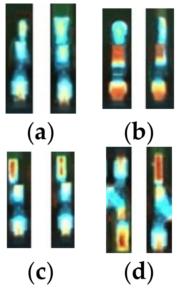
To test the correctness and flexibility of the proposed method and analyze its properties, we used 2 datasets. The solder images dataset (named as DS hereafter), as shown in Figure 1, was provided by an IC manufacturer. It consists of two types of defect images and two types of normal images (Figure 2). All images are scaled to 30 × 120 pixels for processing. The training set consists of 1240 normal samples (558 from the first type, and 682 from the second type); the testing set consists of 2251 defective images and 1814 normal images. No defect samples were used during the training.
We have used another dataset, containing bare PCBs, with different defects, while taking into account that there are no publicly available relevant datasets. This is a set of the PCB images, acquired by a Point Grey FlyCapture camera, setup on industrial manufacturing line. The resolution of each image is 1288 × 964, and the dataset contains 78 samples of normal PCBs, and 155 samples of defective PCBs with the following defect types: scratch, broken edges, extra holes, missing holes, and missing washers. Figure 3 shows a sample of defect-free bare PCB from the PCB dataset. As a preprocessing step, all training and test images were aligned using the SIFT [32] algorithm, and the non-PCB areas of the images were removed, resulting in the images of 1100 × 600 pixels. These PCB images were divided into 66 nonoverlapping patches, forming a grid of 11 × 6 patches of 100 × 100 pixels in each patch. A class number K (from 1 to 66) was assigned to each patch, which corresponds to its grid location on the PCB image. All the samples of the same class, K, had the same layout, with minor variations, due to manufacturing process, and they were not the exact copies of each other. Each of the 66 patches were analyzed separately to verify the correctness of the whole PCB images.
As our method is based on one class classification, the validation dataset will not be used for training process; there are no negative samples in the dataset.

4.2. Model Architecture ane Experiment Description

To perform defect analysis, the model should be able to distinguish between normal and defective patterns. As it is trained only on defect-free samples, the model should be able to identify correctly the repeatable normal patterns. This problem statement assumes learning by using a small number of normal samples only. Commonly accepted way to perform extraction of features from a new data without an exhaustive training is to use transfer learning. In our work, we used VGG16 [33] (and also conducted an experiment with ResNet50 [34], see Section 5), with network weights pre-trained on ImageNet dataset and pre-defined parameters. VGG16 has 16 layers (13 convolutional layers in 5 convolution blocks and 3 fully-connected layers, see Figure 4). It was trained on more than 1 million images to do classification into 1000 categories.
Different approaches can be used to utilize a transfer learning network on a custom dataset; for example, in some cases, the initial layers (the corresponding coefficients) of VGG16 are frozen and the remaining layers weight coefficients are re-trained and adjusted using a custom training set.
This approach is mainly used for supervised transfer learning. The number of classes in the dataset is equal to the number of neurons in the last fully-connected (fc) layer. The original VGG16 architecture (for the input 224 × 224 × 3) has a FC2 layer (Figure 4) of 4096 elements, and the output of flattened layer (after 13 convolutional layers) is a tensor of 25,088 elements.
We compared three model architectures to identify which one is better under certain conditions. The first architecture, hereafter called A1, is comprised of two parts. The initial layers (i.e., convolutional layers) of the pre-trained VGG16 were frozen and used as the first part of feature extraction. Two additional fully-connected (FC, Figure 5) layers were added as the second part of the feature extractor, as it was also done in [35] that implements unsupervised learning network based on simple geometric transformations. We expect that this approach provides additional fine-tuning (according to our custom datasets) of the existing rich feature extraction capability VGG16 network without constructing a custom CNN model from the scratch.
The RotNet model from [35] allows for the complex features’ extraction from the input images without labelling the training data, and the author suggested using convolutional network to recognize 2D-rotations applied to the input data. For example, the input images could be rotated by 0, 90, 180, and 270 degrees, or as an option, can be flipped horizontally or vertically. Then, the ConvNet learns how to recognize geometric transformations. At the same time, by learning the transformation applied, representative features from the augmented dataset are extracted. As a result, the image representation is learned through artificial introduction of transformations classes [35], using an unsupervised learning process by adding to the process the intermediate (semi-) supervised stage. The image understanding incorporated into this rotational ConvNet helps to extract the features essential for the image dataset under analysis, by using “surrogate supervision signals” [35].
After conducting several experiments, we chose the modification of VGG16 (Figure 6), which seems to work successfully in our task. The initial convolutional layers in VGG16 were frozen, and the subsequent fully-connected layers were removed. We have added two fully-connected layers (FC1 and FC2), each containing 1000 neurons (the number chosen arbitrarily), followed by a SoftMax layer with the number of outputs equal to the number of classes.
The frozen VGG16 layers’ output parameters are flattened, which serve as the input to FC1. We arbitrarily decided to use 1000 elements in FC1 and FC2 each, as our PCB images are not so varied by its nature, in comparison with ImageNet images of 1000 classes. The length of dense SoftMax layer corresponds to the number of patches in PCB. The training of the modified network is done using normal PCBs (66 grids per PCB). We tried several ways to organize the training process and force our model to learn semantic image features from patches [36]. The most promising approach appears to be the following:
  • To choose the size of the patch comparable to the size of individual elements, as too small patch size will lead to extra sensitivity to normal minor changes, and too large patch size will result in a lack of discriminative power to detect and localize the defect. The patch size will affect the number of classes K, in which our PCB will be divided.
  • To feed the patches randomly rotated by 0, 90, 180, and 270 degrees to the described configuration of the network.
In our implementation for PCB analysis, the input image (patch) size of 100 × 100 pixels was chosen. It gave us the flatten layer output tensor of 4608 elements (Figure 4) and the number of network parameters (before FC layers) as 14.7M. The number of trainable parameters in FC layers is 5.8M. The network was trained to match the patch (potentially rotated) to its location on PCB, i.e., to match it to the correct number of class K, which is the output of the SoftMax layer, using the categorical cross-entropy loss function. After training the new model by using only the normal patches, we remove the FC2 and the SoftMax layers, and the output of the FC1 layer is used as the feature vector for a given input for the architecture A1. Layers FC1 and FC2 extract different information patterns. Later we will check which layer’s feature vector contains more relevant information about the input image structures to distinguish a patch with a normal design from a defective one. The other architectures (A2 and A0) are the same as A1, with the following modifications: the output feature vectors are output of FC2 (see Figure 5) and FC1 (Figure 4) layers, respectively. In other words, in A0 architecture we use the feature vector (the output of FC1 layer) of the original VGG16 without any training by the RotNet. The difference between A1 and A2 is in the choice of which fully-connected layer outputs to use. The FC1 layer extracts more generic features of the image processed, and FC2 would operate with more specific information. It will be shown that the choice between FC1 and FC2 is crucial. In [35], the authors trained RotNet without usage of transfer learning model as the pre-trained feature extractor, opposite to this article’s proposed approach.
For the training of the class K patches (K from 1 to 66 in this case), we calculate a set of normal signatures (representations) for the class K, containing multidimensional feature vectors. This set defines a cluster, which contains all representations for normal samples for this class. This cluster may consist of disjoint sets. When a patch (belonging to a certain class K) of the testing image is analyzed, the feature vector of the patch is calculated first, and then its distance from the cluster of normal representations of the same class is found. If this distance exceeds a certain threshold, the patch is considered defective. This process is repeated for all the patches of the test image, and the location of a defective patch is marked on the PCB. Currently, the threshold value is set manually and is same for all the classes. The threshold value cannot be defined automatically as it depends on the product itself, and our system has no prior information about the nature of the defects and acceptable deviations.
For dataset DS, we use the same architectures A0, A1, and A2, with classes K = 1:2, which correspond to the number of normal types of solders. Similar to before, only normal images were used for training, the samples were fetched randomly, and the process of calculations was repeated several times for different selections. The overall pipeline of the process is as following. First, a high-quality solder image is captured, which undergoes several pre-processing steps (e.g., background removal, alignment, noise filtering, etc.) to make it more suitable for further processing. This neural network is first trained to extracts features and constructs a set of signatures, which are later used for deciding the presence or absence of a defect.
To calculate the quality of model on testing dataset, F1 and MCC performance measures have been used, as follows:
F 1   Score   = 2 Recall     Precision Recall   +   Precision
  • where, Precision   = TP TP + FP , Recall   = TP TP + FN
  • and MCC   = TP TN FP FN TP + FP TP + FN TN + FP TN + FN
  • and TP, TN, FP, and FN are the numbers of true positive, true negative, false positive, and false negative, respectively. The F1 score is the harmonic mean of precision and recall (sensitivity). The Matthews correlation coefficient (MCC) [37] is a measure of the quality of binary (two-class) classifications. It considers true and false positives and negatives and is generally regarded as a balanced measure that can be used, even if the classes are of very different sizes. The MCC is a correlation coefficient between the observed and predicted binary classifications. It returns a value between −1 and +1. A coefficient of +1 represents a perfect prediction, 0 represents no better than random prediction, and −1 indicates total disagreement between prediction and observation. The MCC score is high only if the classifier is doing well on both the negative and positive samples.
To find out how the number of cases for training of the network affects the final accuracy at testing stage, we conducted the following experiments (the same for datasets DS and PCB). For architectures A1 and A2, as a training dataset, we used a subset of the whole dataset, with increasing number of samples and calculate MCC for the result. As a benchmark for comparison, we chose to use the architecture A0, where the training was done using all the available normal samples. It would allow us to check whether and when fine-tuning, using [35], provides better performance for a small training set.

5. Findings

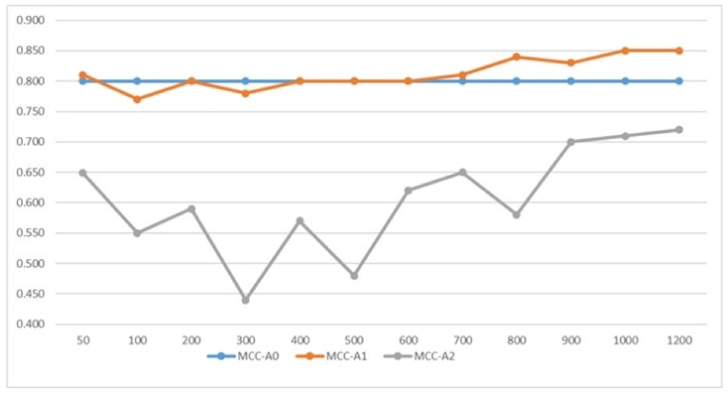
The code of this experiment was implemented in Python using Keras and TensorFlow frameworks. The result of localization of PCB defects found in PCB is demonstrated in Figure 6. For solders, the generated output was the classification of sample into “defect” or “normal”. The running time for processing of one image is less than 0.5 s at computer with CPU i7, RAM 16GB, and GPU Nvidia GeForce GTX 1060 6GB. The performance measures of defect detection for different architectures are provided in Table 1 and Table 2 for solders and in Table 3 and Table 4 for PCBs. Figure 7 and Figure 8 depict the behavior of MCC for A0, A1, and A2 for solders and PCBs, respectively.
Among all the types of defects for PCB dataset, the analysis of the results showed that for missing washers and surface texture defects, the correctness of detection was extremely low, around 0. Using the ResNet50 [34] network, instead of VGG16, for the method described did not change the behavior of the results.

6. Discussion and Implications

Technical images (such as images of PCBs and solders) demonstrate a pre-defined design and low variability, so the detailed information about their design is crucial for the detection of defects. In unsupervised learning, unlabeled samples are used to extract information about possible patterns in data. Transfer learning technique is utilized to re-use knowledge learned by a network in some other but related area. In our experiment, we used VGG16 as a feature extractor in several ways (A0, A1, and A2), using it either alone or with the RotNet fine-tuning, to compare how network would learn the salient features from the data and use them for learning of normal patterns in data.
Unsupervised training should extract intrinsic image features, without domain-specific knowledge. The patterns learned are based on features from pre-trained ImageNet. We assume that the space of features, extracted by ImageNet, are rather comprehensive. The approach A0 analyzes whether we could use the features from ImageNet, without fine-tuning. The approaches A1 and A2 use RotNet fine-tuning upon transfer learning to find a subspace of broad in scope ImageNet features that more efficiently represents the features of our image set. The difference between approaches A1 and A2 is that the former one exploits more generic features of the image, and the latter one uses more specific information after fine-tuning.
The comparison of signatures of normal samples and sample to analyze is based on assumption that the transformation of input image into the signature possesses the property of continuity in feature space. In the consequence, two alike images (having nearly the same characteristics) will be mapped to feature vectors in the same small vicinity. However, if an image contains a defect, its signature should be located far from the cluster of the defect-free samples.
In case of solder dataset DS, the MCC-A1 crossed the plot of MCC-A0 (pretrained VGG16 neural network without RotNet fine-tuning) when the number of training samples was above 600 (Figure 7, Table 1 and Table 2). MCC-A2 is below both plots. We can conclude that at some stage the fine-tuning facilitates better extraction of common normal patterns from the images.
For PCB dataset (Figure 8, Table 3 and Table 4), the behavior of MCC-A1 and MCC-A2 is the same; the first one is above the second. On the contrary to Figure 7, there is no crossing of MCC-A0 and MCC-A1, i.e., the quality of defect detection for fine-tuned network is worse than for untuned one. It could be explained by considering the number of samples in the DS and PCB sets. In case of PCB dataset, a very small number of training samples and rather large number of parameters of layers FC1 and FC2 to be trained causes the following problem. The back-propagation algorithm could not reach a global optimum for thousands of trainable parameters, due to insufficient number of training samples. It does not learn much as a small number of input parameters cannot be used for optimization of a much larger number of network-tunable parameters. As soon as the number of training samples grows, the results of the optimization keep getting better.
The more normal cases are used for training, the more successful fine-tuning becomes, and at some stage MCC-A0 goes under MCC-A1, as Figure 7 demonstrates. In both cases MCC-A1 is above MCC-A2. The similar observation was also made in [35]. The reason is, the RotNet fine-tuning creates artificial labels and trains the network to learn and to extract the features related to these artificial classes. As the result, the earlier located fully-connected layer FC1 (used in model A1) extracts more generic features of the dataset images. The next layer FC2 (used in A2) is tuned to extract features associated to artificially introduced class labels (related to transformations of rotation), and not to the properties of the dataset itself. This observation could explain the manifested difference in behavior of MCC-A1 and MCC-A2. Hence, usage of dataset specific features FC1 allowed to make a better decision on presence of a defect, in comparison with transformation specific features FC2. The model A 0 uses the unaltered features, extracted by VGG16 and trained on ImageNet. These features are not customized for our dataset and demonstrate a baseline accuracy.
Figure 7 and Figure 8 demonstrate that the accuracy of models A1 and A2 changes with the grow of the number of training samples. At some level, the information extracted by RotNet will allows to outperform the baseline accuracy (ref. Figure 7).
Referring to widely used statistical “rule of thumb” [38], which recommends for reliable estimates to have at least 40 to 60 times as many cases as variables that are relevant; in order to explain an outcome variable, we could speculate about the number of relevant features (variables). We could hypothesize that the number of relevant features to detect defect in solders should be more than 10 (as only when the number of samples is above 600, the fine-tuning starts showing better result than the baseline MCC-A0), and for PCB dataset the analysis of rather small number of features would allow detection of above 85 percent of defects (as MCC-A0 shows the accuracy above 85 percent based on only 78 samples). We must emphasize that these conclusions are purely speculative and are based on the mentioned “rule of thumb”.
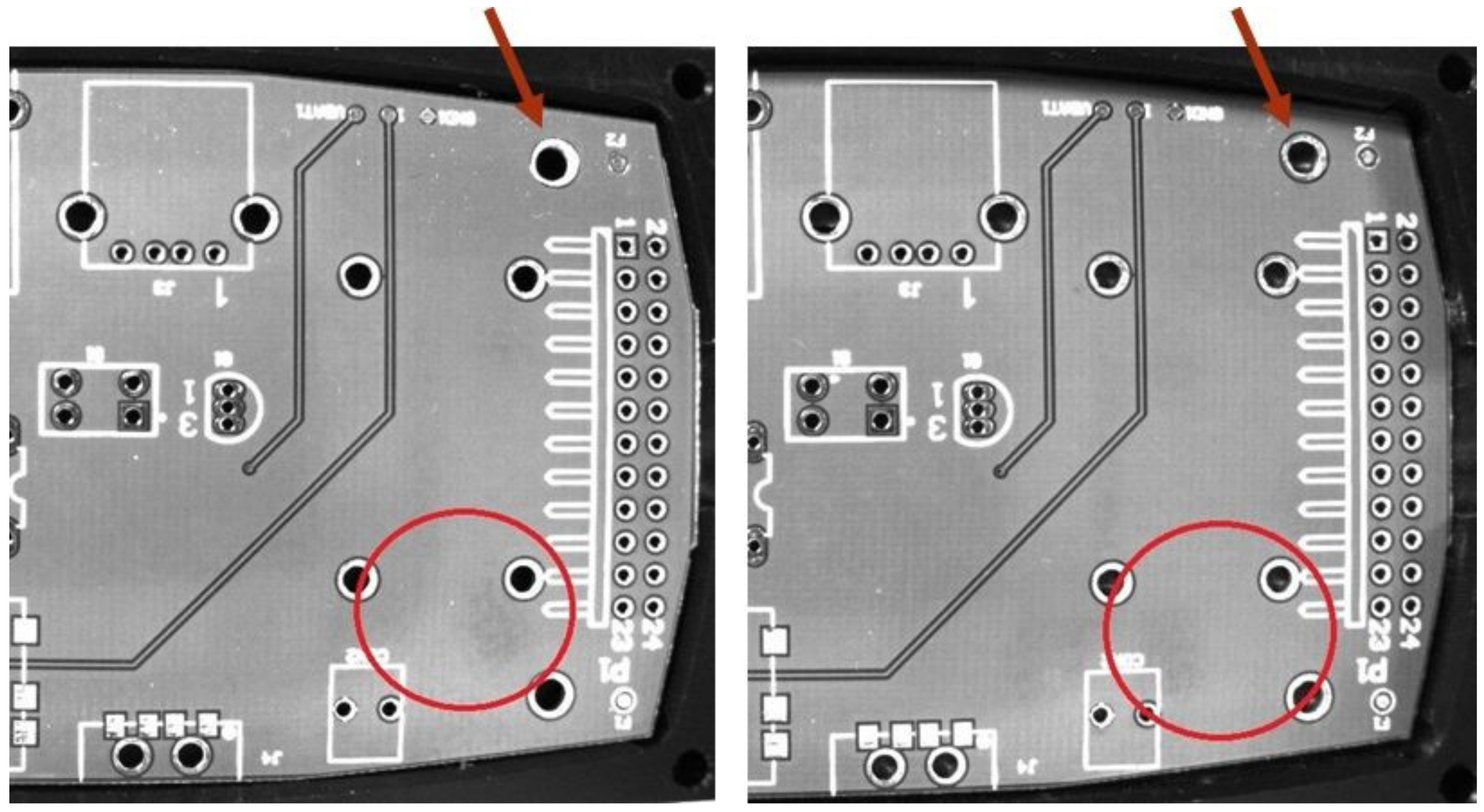
PCB defects were internally divided into two groups: non-texture defect (scratch/abrasion/broken edge/missing and extra hole) vs. texture defects (washers and surface false alarms). Washers were included into texture defects, due to the observation that the presence or absence of a washer could be distinguished only by the texture of the rim (Figure 9). As it was mentioned before, texture defect detection was unsatisfactory due to the fact that training on a limited number of samples could not structure the expected way the information provided. The performance has been poor, due to the fact that the training set did not contain enough variety of “normal” texture/background samples; therefore, any “normal” sample is detected as “defective” if the pattern was not included in the training. The reason for this is in the inherent nature of unsupervised learning, which checks for any pattern not seen before (theoretically infinite), as opposed to supervised learning, which looks for a pattern already seen before (finite only).
In some cases, there is a change of the shadows of the background (Figure 9). Limited number of training examples make network to ignore these features. We assume that the absence of some non-prominent feature (similar to the rather mild change of gradient of the background) in normal data makes the network not to be sensitive to small variations and, hence, ignore such manifestations. We also could assume that for unsupervised learning based on small number of samples, only the “big” features (high gradient image features, such as edges, corners, etc.) are considered, and not the texture of the image. One of the potential ways to overcome this problem is to increase the number of training cases to force the network to learn more about normal texture patterns, as shown in [39]. For a large number of normal cases (that is not usually a problem for mass production line, especially for six sigma processes in manufacturing) the variability of normal cases will be caught much better, and it is the way for better defect detection accuracy, especially for texture defects. A small number of normal cases for texture type of defect detection would result in a high number of false decisions.
A usual requirement for process of learning is not to come to overfitted model. The learning should result in useful pattern extraction from data, rather than in “memorizing”. It ensures a better prediction performance for unseen before data. If the image has a pre-defined design (e.g., technical image), the situation might be somehow different. Along with data pattern extraction, to make model remembering the design patterns could make possible to train the network to detect non-textural underlying relevant structures with a limited number of training samples.
The usage of transfer learning allows for escaping a massive training with a huge data volume and creates a “library” of possible patterns, which could be used to extract important features from a small dataset. The defect detection power of the model highly depends on training set representative power (i.e., how typical and comprehensive the training samples for the analyzed class of objects).

Analysis of Results and Future Work

One of the open questions in deep learning is ‘how to choose a necessary amount of information for network training’. The current approach “the more the better” does not set any limit on how many samples are necessary to make network to learn the semantic of the domain area. In our work, we got an initial result on the accuracy of the neural network defect detection for different scales of numbers of samples for training. The current limitation of our approach is the following: our investigation is based on a limited number of datasets (solders and PCBs), and the datasets have to have small variability of data, intrinsic for technical images.
We proposed an approach based on transfer learning (to reduce the amount of training by usage of a pre-trained network) and employed fine-tuning, based on RotNet, to analyze for what number of samples this fine-tuning is beneficial. We found that for a very small dataset and complex patterns of salient data features, the fine-tuned stage of learning does not help with extraction of robust knowledge patterns from the training data. For an extremely small data set, the more beneficial approach is to use the feature extractor, provided by a transfer learning model without fine-tuning. If the number of normal samples is not a problem, the fine-tuning results will outperform the results received by transfer learning approach as a larger volume of training data could make the model more successful in the extraction of the implicit patterns. In case the training data does not provide comprehensive information for the network, the connections built in the network might be different from the expected by a human expert, as the model would “see” different features, unexpected by human with a relevant domain knowledge.
The presented method allows us to conduct AOI, even before the actual manufacturing starts without collecting a big dataset of normal and defective samples. Our analysis requires only a small number of normal samples, and we found that the defect detection can be performed well on a smooth background; however, in cases where the defect manifests as a change of texture, the detection can be less accurate.
With the current accuracy, the approach is not industry-ready, but could be potentially used for OCC analysis of different type of technical images, which should possess the same structure, design, or composition. It would allow for checking the agreement with design and detect violation of expected structure, without specifying, in advance, the possible classes of defects and their specific features to be analyzed. The method would improve the robustness of the AOI process to detect rare and previously unseen defects.
The architecture proposed also opens a possibility of a “one sample defect training” when a new type of defect could be introduced by a unique defect sample only. The signature of this sample will become a center of a new cluster for a specific type of defect. It will facilitate defect clustering into different classes.
For two different datasets (solders and bare PCBs), the performance of the approach could be considered as quite promising. However, for texture defects in PCBs, the performance was poor, since the training set did not contain enough variety of “normal” texture samples; therefore, any “normal” sample is detected as “defective” if the pattern was not included in the training. With the increase of normal cases (that is not usually a problem for mass production line), the variability of normal cases will be caught much better and is the way for better defect detection accuracy. In future, it would be interesting to analyze:
  • How to detect whether the sample is representative or not adding much to training;
  • How to form a representative set of samples;
  • Whether the traditional computer vision techniques could be combined with machine learning to improve the accuracy.
The additional analysis of the method robustness and applicability to different defect detection will be a topic of future work.

7. Conclusions

For defect detection analysis, a method based on transfer learning and training, utilizing a small number of defect-free samples, was proposed. It allows us to detect and locate patterns that were previously unseen in the training samples. We also analyzed and discussed the correspondence between the number of training samples and the performance of the model, as well as investigated under which circumstances the fine-tuning does not add to the accuracy, so the feature extractor, based on the non-adjusted pre-trained model, would show better results. To the best of our knowledge, currently there are no works available on defect detection based on the transfer learning approach and unsupervised learning using a small number of samples.
The proposed method is an initial attempt to conduct the detection of unclassified in advance detects. It is mainly an example of an open innovation approach [40] to use a deep learning technology to address a DMAIC challenge in AOI.

Author Contributions

Development of methodology and conceptualization, all the authors; software and validation, I.V. and A.M.; writing, I.V., A.M. and A.S.; data acquisition and preparation, A.M. and W.D.; project administration, M.E. and A.S. All authors have read and agreed to the published version of the manuscript.

Funding

This work was conducted within the Delta–NTU Corporate Lab for Cyber-Physical Systems, with funding support from Delta Electronics Inc. and the National Research Foundation (NRF) Singapore, under the Corp Lab@University Scheme.

Data Availability Statement

Not applicable, the study does not report any data.

Conflicts of Interest

The authors declare no conflict of interests.

References

  1. Moganti, M.; Ercal, F.; Dagli, C.H.; Tsunekawa, S. Automatic PCB Inspection Algorithms: A Survey. Comput. Vis. Image Underst. 1996, 63, 287–313. [Google Scholar] [CrossRef] [Green Version]
  2. Anitha, D.B.; Rao, M. A survey on defect detection in bare PCB and assembled PCB using image processing techniques. In Proceedings of the 2017 International Conference on Wireless Communications, Signal Processing and Networking (WiSPNET), Chennai, India, 22–24 March 2017; pp. 39–43. [Google Scholar]
  3. Taha, E.M.; Emary, E.; Moustafa, K. Automatic optical inspection for PCB manufacturing: A survey. Int. J. Sci. Eng. Res. 2014, 5, 1095–1102. [Google Scholar]
  4. Drury, C.G.; Sinclair, M.A. Human and Machine Performance in an Inspection Task. Hum. Factors J. Hum. Factors Ergon. Soc. 1983, 25, 391–399. [Google Scholar] [CrossRef]
  5. Huang, S.-H.; Pan, Y.-C. Automated visual inspection in the semiconductor industry: A survey. Comput. Ind. 2015, 66, 1–10. [Google Scholar] [CrossRef]
  6. Zhang, C.; Shi, W.; Li, X.; Zhang, H.; Liu, H. Improved bare PCB defect detection approach based on deep feature learning. J. Eng. 2018, 2018, 1415–1420. [Google Scholar] [CrossRef]
  7. Wu, W.-Y.; Wang, M.-J.J.; Liu, C.-M. Automated inspection of printed circuit boards through machine vision. Comput. Ind. 1996, 28, 103–111. [Google Scholar] [CrossRef]
  8. Eun, H.Y.; Seung, H.P.; Cheong-Sool, P.; Jun-Geol, B. Feature-learning-based printed circuit board inspection via speeded-up robust features and random forest. Appl. Sci. 2018, 8, 932. [Google Scholar]
  9. Kim, H.W.; Yoo, S.I. Defect detection using feature point matching for non-repetitive patterned images. Pattern Anal. Appl. 2012, 17, 415–429. [Google Scholar] [CrossRef]
  10. Dahlgaard-Park, S.M. Define, Measure, Analyze, Improve, and Control (DMAIC) Process. In The SAGE Encyclopedia of Quality and the Service Economy; SAGE Publications, Inc.: New York, NY, USA, 2015; Volume 1, pp. 141–143. [Google Scholar]
  11. Tikhe, C. Metal surface inspection for defect detection and classification using Gabor Filter. Int. J. Innov. Res. Sci. Eng. Technol. 2014, 3, 13702. [Google Scholar]
  12. Timm, F.; Barth, E. Non-parametric texture defect detection using Weibull features. In Proceedings of the IS&T/SPIE Electronic Imaging, San Francisco, CA, USA, 23–27 January 2011. [Google Scholar]
  13. Wang, Z. Image quality assessment: From error visibility to structural similarity. IEEE Trans. Image Process. 2004, 13, 600–612. [Google Scholar] [CrossRef] [Green Version]
  14. Carro, R.C.; Larios, J.-M.A.; Huerta, E.B.; Caporal, R.M.; Cruz, F.R. Face Recognition Using SURF. In Proceedings of the Intelligent Computing Theories and Methodologies, Fuzhou, China, 20–23 August 2015; pp. 316–326. [Google Scholar]
  15. Suvdaa, B.; Ahn, J.; Ko, J. Steel surface defects detection and classification using SIFT and voting strategy. Int. J. Softw. Eng. Appl. 2012, 6, 161–166. [Google Scholar]
  16. Khalid, N. An algorithm to group defects on printed circuit board for automated visual inspection. Int. J. Simul. Syst. Sci. Technol. 2008, 9, 1–10. [Google Scholar]
  17. Heriansyah, R.; Al-attas, S.A.R.; Munim, M. Neural network paradigm for classification of defects. J. Teknol. 2003, 39, 87–103. [Google Scholar] [CrossRef] [Green Version]
  18. Wu, X.; Cao, K.; Gu, X. A Surface Defect Detection Based on Convolutional Neural Network. In Proceedings of the International Conference on Computer Vision Systems, Lecture Notes in Computer Science, Shanghai, China, 13–14 July 2017; pp. 185–194. [Google Scholar]
  19. Masci, J.; Meier, U.; Ciresan, D.; Schmidhuber, J.; Fricout, G. Steel defect classification with Max-Pooling Convolutional Neural Networks. In Proceedings of the 2012 International Joint Conference on Neural Networks (IJCNN), Brisbane, QLD, Australia, 10–15 June 2012; pp. 1–6. [Google Scholar]
  20. Wang, T.; Chen, Y.; Qiao, M.; Snoussi, H. A fast and robust convolutional neural network-based defect detection model in product quality control. Int. J. Adv. Manuf. Technol. 2018, 94, 3465–3471. [Google Scholar] [CrossRef]
  21. Wei, X.; Yang, Z.; Liu, Y.; Wei, D.; Jia, L.; Li, Y. Railway track fastener defect detection based on image processing and deep learning techniques: A comparative study. Eng. Appl. Artif. Intell. 2019, 80, 66–81. [Google Scholar] [CrossRef]
  22. Chaudhary, V.; Dave, I.R.; Upla, K.P. Automatic visual inspection of printed circuit board for defect detection and classification. In Proceedings of the 2017 International Conference on Wireless Communications, Signal Processing and Networking (WiSPNET), Chennai, India, 22–24 March 2017; pp. 732–737. [Google Scholar]
  23. Sun, J.; Wyss, R.; Steinecker, A.; Glocker, P. Automated fault detection using deep belief networks for the quality inspection of electromotors. Tech. Mess. 2014, 81, 255–263. [Google Scholar] [CrossRef] [Green Version]
  24. Zhang, M.; Wu, J.; Lin, H.; Yuan, P.; Song, Y. The Application of One-Class Classifier Based on CNN in Image Defect Detection. Procedia Comput. Sci. 2017, 114, 341–348. [Google Scholar] [CrossRef]
  25. Mei, S.; Wang, Y.; Wen, G. Automatic Fabric Defect Detection with a Multi-Scale Convolutional Denoising Autoencoder Network Model. Sensors 2018, 18, 1064. [Google Scholar] [CrossRef] [Green Version]
  26. Hu, G.; Huang, J.; Wang, Q.; Li, J.; Xu, Z.; Huang, X. Unsupervised fabric defect detection based on a deep convolutional generative adversarial network. Text. Res. J. 2020, 90, 247–270. [Google Scholar] [CrossRef]
  27. Masci, J.; Meier, U.; Cireşan, D.; Schmidhuber, J. Stacked convolutional auto-encoders for hierarchical feature extraction. In Proceedings of the ICANN’11: Proceedings of the 21th International Conference on Artificial Neural Networks, Espoo, Finland, 14–17 June 2011. [Google Scholar]
  28. Mujeeb, A.; Dai, W.; Erdt, M.; Sourin, A. Unsupervised Surface Defect Detection Using Deep Autoencoders and Data Augmentation. In Proceedings of the 2018 International Conference on Cyberworlds (CW), Singapore, 3–5 October 2018; pp. 391–398. [Google Scholar]
  29. Zhao, B.; Feng, J.; Wu, X.; Yan, S. A survey on deep learning-based fine-grained object classification and semantic segmentation. Int. J. Autom. Comput. 2017, 14, 119–135. [Google Scholar] [CrossRef]
  30. Koch, G.; Zemel, R.; Salakhutd, R. Siamese Neural Networks for One-Shot Image Recognition. In Proceedings of the ICML Deep Learning Workshop, Lille, France, 6–11 July 2015. [Google Scholar]
  31. Vinyals, O.; Blundell, C.; Lillicrap, T.; Kavukcuoglu, K.; Wierstr, D. Matching Networks for One Shot Learning. In Proceedings of the NIPS—30th International Conference on Neural Information Processing Systems, Barcelona, Spain, 9–12 December 2016. [Google Scholar]
  32. Lowe, D. Object Recognition from Local Scale-Invariant Features. In Proceedings of the Seventh IEEE International Conference on Computer Vision, Corfu, Greece, 20–25 September 1999. [Google Scholar]
  33. Simonyan, K.; Zisserman, A. Very deep convolutional networks for large-scale image recognition. arXiv 2014, arXiv:1409.1556. [Google Scholar]
  34. He, K.M.; Zhang, X.Y.; Ren, S.Q.; Sun, J. Deep Residual Learning for Image Recognition. In Proceedings of the IEEE Conference on Computer Vision and Pattern Recognition, Las Vegas, NV, USA, 27–30 June 2016; pp. 770–778. [Google Scholar] [CrossRef] [Green Version]
  35. Gidaris, S.; Singh, P.; Komodakis, N. Unsupervised representation learning by predicting image rotations. In Proceedings of the ICLR 2018, Vancouver, BC, Canada, 30 April–3 May 2018. [Google Scholar]
  36. Volkau, I.; Mujeeb, A.; Wenting, D.; Marius, E.; Alexei, S. Detection Defect in Printed Circuit Boards using Unsupervised Feature Extraction Upon Transfer Learning. In Proceedings of the 2019 International Conference on Cyberworlds (CW), Kyoto, Japan, 2–4 October 2019; pp. 101–108. [Google Scholar]
  37. Matthews, B. Comparison of the predicted and observed secondary structure of T4 phage lysozyme. Biochim. Biophys. Acta BBA Protein Struct. 1975, 405, 442–451. [Google Scholar] [CrossRef]
  38. Barcikowski, R.S.; Stevens, J.P. A Monte Carlo Study of the Stability of Canonical Correlations, Canonical Weights and Canonical Variate-Variable Correlations. Multivar. Behav. Res. 1975, 10, 353–364. [Google Scholar] [CrossRef]
  39. Geirhos, R.; Rubisch, P.; Michaelis, C.; Bethge, M.; Wichmann, F.A.; Brendel, W. ImageNet-Trained CNNs Are Biased towards Texture; Increasing Shape Bias Improves Accuracy and Robustness. arXiv 2018, arXiv:1811.12231. [Google Scholar]
  40. Baierle, I.C.; Benitez, G.B.; Nara, E.O.B.; Schaefer, J.L.; Sellitto, M.A. Influence of Open Innovation Variables on the Competitive Edge of Small and Medium Enterprises. J. Open Innov. Technol. Mark. Complex. 2020, 6, 179. [Google Scholar] [CrossRef]
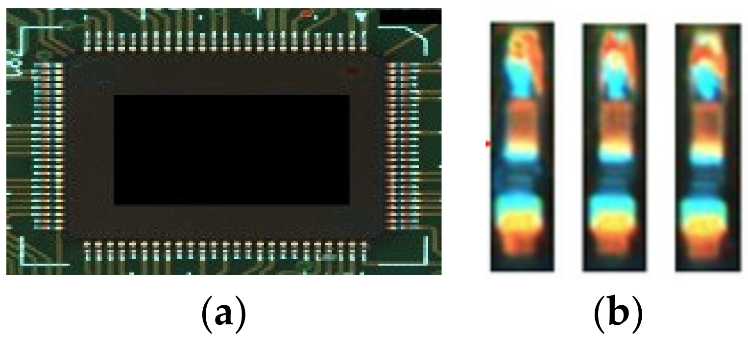
Figure 1. (a) PCB with solder joints; (b) Extracted soler joints.
Futureinternet 14 00008 g001
Figure 2. (a) normal (type 1); (b) normal (type2); (c) defect (type1); (d) defect (type 2).
Futureinternet 14 00008 g002
Figure 3. Defect-free printed circuit board.
Futureinternet 14 00008 g003
Figure 4. VGG16 model.
Futureinternet 14 00008 g004
Figure 5. Modified VGG16 deep network (architecture A1).
Futureinternet 14 00008 g005
Figure 6. The number in each patch is a distance to the normal cluster. Blue number areas are identified as normal, red ones are identified defective (the distance is above a threshold).
Futureinternet 14 00008 g006
Figure 7. Solder dataset: MCC for A0, A1, and A2.
Futureinternet 14 00008 g007
Figure 8. PCB dataset: MCC for A0, A1, and A2.
Futureinternet 14 00008 g008
Figure 9. Missing (left) and present (right) washers (marked by arrows). Non-uniformed background looks like ghost images (marked by circles).
Futureinternet 14 00008 g009
Table 1. Defect detection of solders for A0.
Samples F1 MCCRecallPrecision
12000.870.800.850.89
Table 2. Defect detection of solders for A1 and A2.
A1A2
Samples F1 MCCRecallPrecisionF1MCCRecallPrecision
500.880.810.870.890.810.650.980.69
1000.820.770.890.760.770.550.940.65
2000.860.800.820.900.770.590.920.66
3000.870.780.880.860.680.440.760.61
4000.870.800.830.910.760.570.890.67
5000.880.800.850.910.740.480.940.61
6000.880.800.870.890.740.620.860.65
7000.880.810.870.890.790.650.880.72
8000.900.840.910.890.760.580.830.70
9000.890.830.890.890.790.700.840.74
10000.900.850.910.890.830.710.900.77
12000.900.850.910.890.840.720.930.77
Table 3. Defect detection of PCBs for A0.
Samples F1 MCCRecallPrecision
780.880.870.900.87
Table 4. Defect detection of PCBs for A1 and A2.
A1A2
Samples F1 MCCRecallPrecisionF1MCCRecallPrecision
80.800.780.800.800.770.760.790.76
160.830.820.850.810.810.800.820.80
240.840.830.890.790.820.810.830.81
320.830.820.860.810.820.810.840.80
400.860.850.890.830.830.820.880.80
480.830.820.820.840.810.800.840.78
560.830.820.820.840.810.790.840.78
640.830.820.910.770.820.810.850.79
720.840.830.830.840.800.780.860.75
780.830.820.870.800.790.780.880.72
Publisher’s Note: MDPI stays neutral with regard to jurisdictional claims in published maps and institutional affiliations.