1. Introduction
Numerous recent studies have focused on oxide semiconductors, such as amorphous indium–gallium–zinc oxide (a-IGZO). Because of their high mobility and transparency, these semiconductors have been applied as active channel layers in thin-film transistors (TFTs) [
1,
2,
3]. Regarding traditional silicon-based TFTs, amorphous silicon (a-Si:H) exhibits low carrier mobility (0.5–1 cm
2/V·s), whereas polycrystalline silicon (poly-Si) requires high-temperature fabrication processes (>500 °C) [
4,
5]. Conversely, a-IGZO TFTs can be fabricated on plastic substrates at low temperatures and exhibit excellent electrical characteristics [
6,
7].
The a-IGZO TFTs that are employed in displays are typically fabricated using back-channel-etching structure and five photomasks, including the definition of an etching-stop (ES) layer to protect the a-IGZO active layer from damage caused by etching the source/drain (S/D) electrodes [
8]. However, thin-film transistors (TFTs) that involve an ES require a misalignment margin for the ES to ensure the good contact between the S/D and the induced channel; thus, high parasitic capacitances which between the source/drain (S/D) electrodes and gate electrode (
Cgd,
Cgs) could occur, decreasing the operational speed of the TFT circuit [
9].
To reduce the parasitic capacitance of TFTs with ES, Geng
et al. proposed a self-aligned process employing backside-ultraviolet (BUV) exposure through a metal-gate-electrode to define the ES area, thereby reducing the misalignment margin [
10]. However, four or five-photo-masks were used during fabrication. To reduce the fabrication costs and prevent hydrogen-based material from affecting the a-IGZO active layer during ES deposition [
11], Uhm
et al. proposed a two-photo-mask scheme that employed a gray-tone photomask to fabricate TFT devices [
12]; however, the lack of an ES layer can cause damage to the a-IGZO active island when etching the S/D electrodes. In addition, the ZnO TFT with three photomasks was also proposed [
13]. However, the continuous etching of S/D metal, IGZO and gate insulator were not considered in that report. The
Table 1 lists the comparisons between these reports and this study.
Table 1.
Summary of indium–gallium–zinc oxide (IGZO)-based thin-film transistors (TFTs) using different process.
Table 1.
Summary of indium–gallium–zinc oxide (IGZO)-based thin-film transistors (TFTs) using different process.
| Reference | Channel material | Self-aligned | Mask number | S/D Etching damage | a-IGZO Degradation due to ES-layer deposition |
|---|
| [10] | IGZO | Yes | 4 | No | Yes |
| [12] | IGZO | No | 2 | Yes | No |
| [13] | ZnO | Yes | 3 | No | No |
| this work | IGZO | Yes | 2 | No | No |
2. Device Fabrication
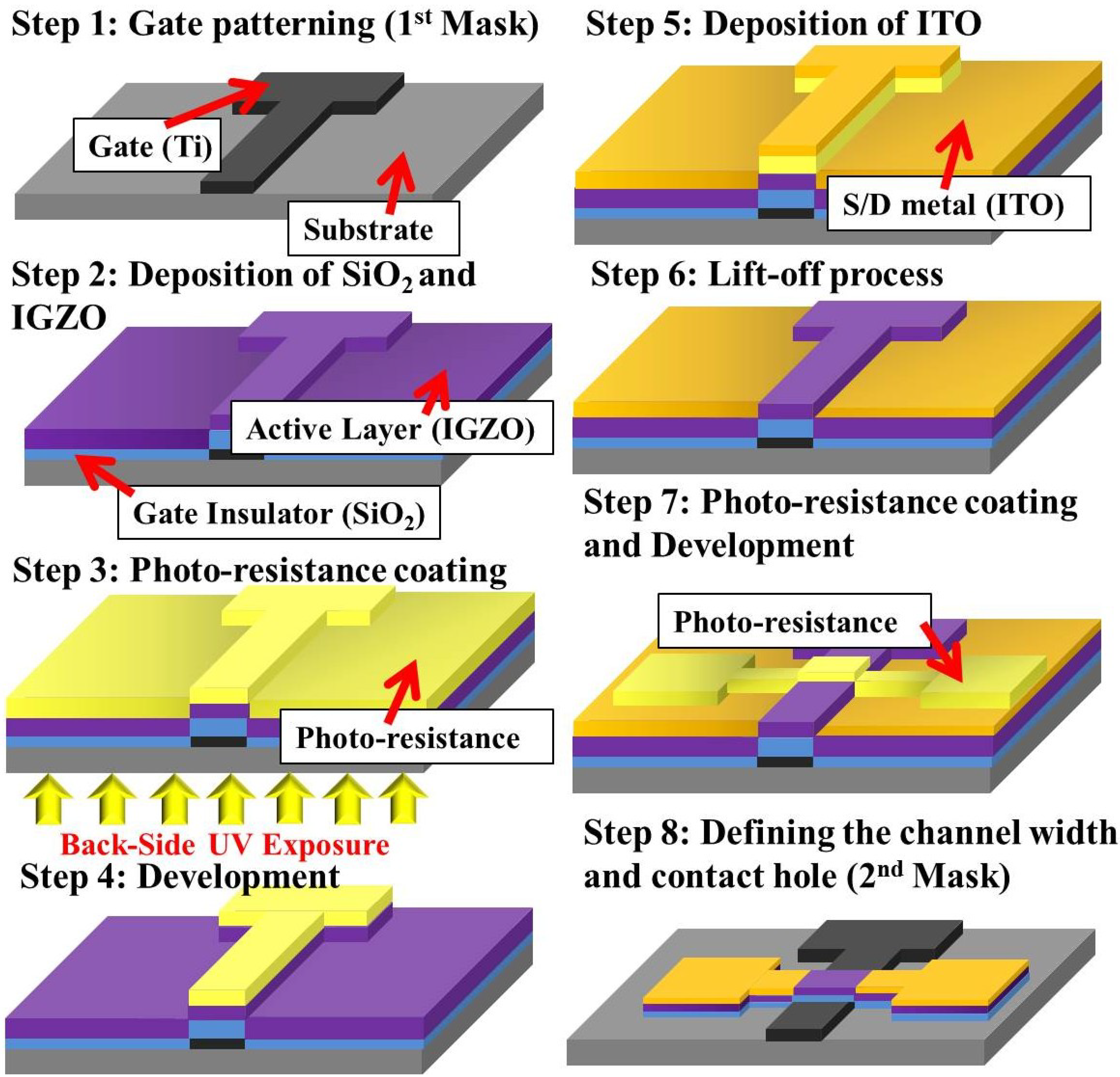
Figure 1 shows the proposed two-mask process for fabricating a-IGZO TFTs. A 160-nm-thick Ti layer was first deposited onto a glass substrate by using thermal evaporation, and then patterned to form the gate electrode by the first photomask. Subsequently, a 200-nm-thick silicon dioxide (SiO
2) was deposited using plasma enhanced chemical vapor deposition at 300 °C, forming the gate insulator. Subsequently, a 20-nm a-IGZO layer was deposited at 200 °C by a radio frequency (RF) sputtering system using a target of In:Ga:Zn = 1:1:1 in atomic ratio. The backside-lift-off (BLO) process is detailed as follows. First, a photo-resist (PR) was spin-coated onto IGZO and subjected to BUV exposure through the Ti gate as a photomask, as shown in
Figure 1. Second, a 350-nm-thick Indium-Tin Oxide (ITO) was deposited using RF sputtering. Subsequently, the BLO scheme was applied to define the channel length of the self-aligned structure. Following the BLO process, the second photomask were used to define the channel width. Reactive-ion etching (RIE) with CF
4 gas was used to continuously etch ITO, IGZO and SiO
2 under the pressure of 80 mtorr. Finally, the devices were annealed at 200 °C for 30 min in a vacuum chamber. To compare the proposed devices, we used a traditional four-photo-mask process to fabricate devices that exhibited various overlap lengths between the gates and S/D electrodes [
11].
Figure 1.
Two-Mask process flow of amorphous indium–gallium–zinc–oxide (a-IGZO) thin-film transistors (TFTs) with self-aligned structure.
Figure 1.
Two-Mask process flow of amorphous indium–gallium–zinc–oxide (a-IGZO) thin-film transistors (TFTs) with self-aligned structure.
3. Results and Discussion
In this study, a new two-photo-mask process with continuous-etching scheme was proposed for fabricating a-IGZO TFTs that exhibit self-aligned structures without ES layers. The ITO metal was designed as S/D metal to meet the requirement of the continuous etching process. Thus, S/D metal, IGZO and gate insulator can simultaneously be etched. Combining the BUV exposure and backside-lift-off (BLO) schemes can not only prevent the damage when etching the S/D electrodes but also reduce the number of photo-masks required during fabrication and minimize the parasitic capacitance at same time.
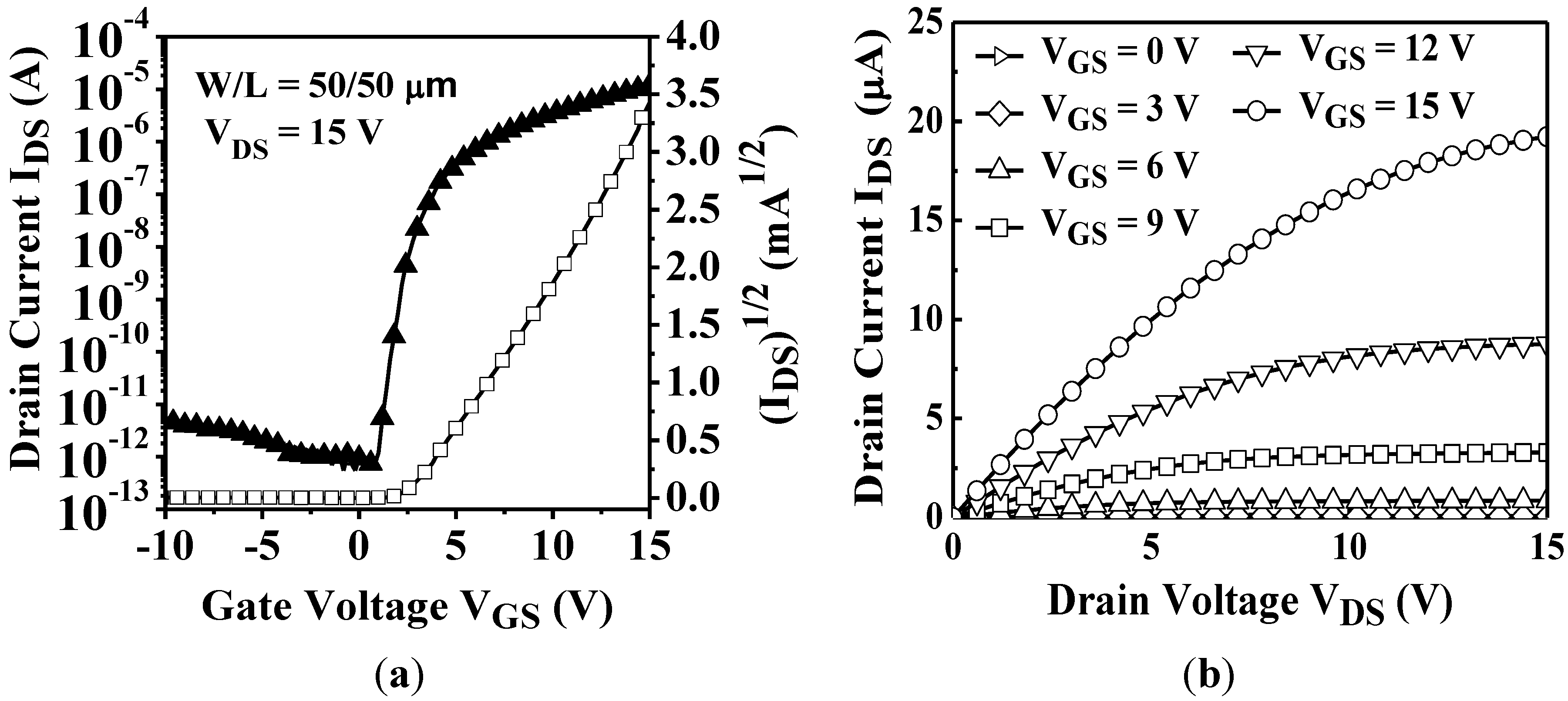
Figure 2a,b shows the transfer and output characteristics of the proposed a-IGZO TFTs with self-aligned structure for channel width (W) of 50 μm and channel length (L) of 50 μm, respectively. A total of 20 devices were measured at various positions across the substrate by using a semiconductor parameter analyzer (HP4145B Hewlett Packard, Palo Alto, CA, USA). The extracted saturation field-effect mobility (μ
sat), threshold voltage (
VT), subthreshold swing (
S), and on-off current ratio (
Ion/
Ioff) are 9.50 cm
2/V·s, 3.39 V, 0.3 V/decade, and 4 × 10
7, respectively. μ
sat and
VT are extracted from the slope and linear extrapolations of the plot of the square root of the drain current as a function of the gate voltage, respectively [
14,
15,
16]. Moreover, the output characteristics show that current crowding did not occur in the linear region to reveal the contact resistance of the S/D regions can satisfy the requirement of transportation current [
17].
Figure 2.
(a) Transfer characteristic (VDS = 15 V) and (b) output characteristic of a-IGZO TFT with self-aligned structure (W/L = 50 μm/50 μm).
Figure 2.
(a) Transfer characteristic (VDS = 15 V) and (b) output characteristic of a-IGZO TFT with self-aligned structure (W/L = 50 μm/50 μm).
The devices were fabricated using the traditional four-photo-mask process, yielding various overlap lengths (
Lov = 100 and 200 μm) between the gate and S/D electrodes.
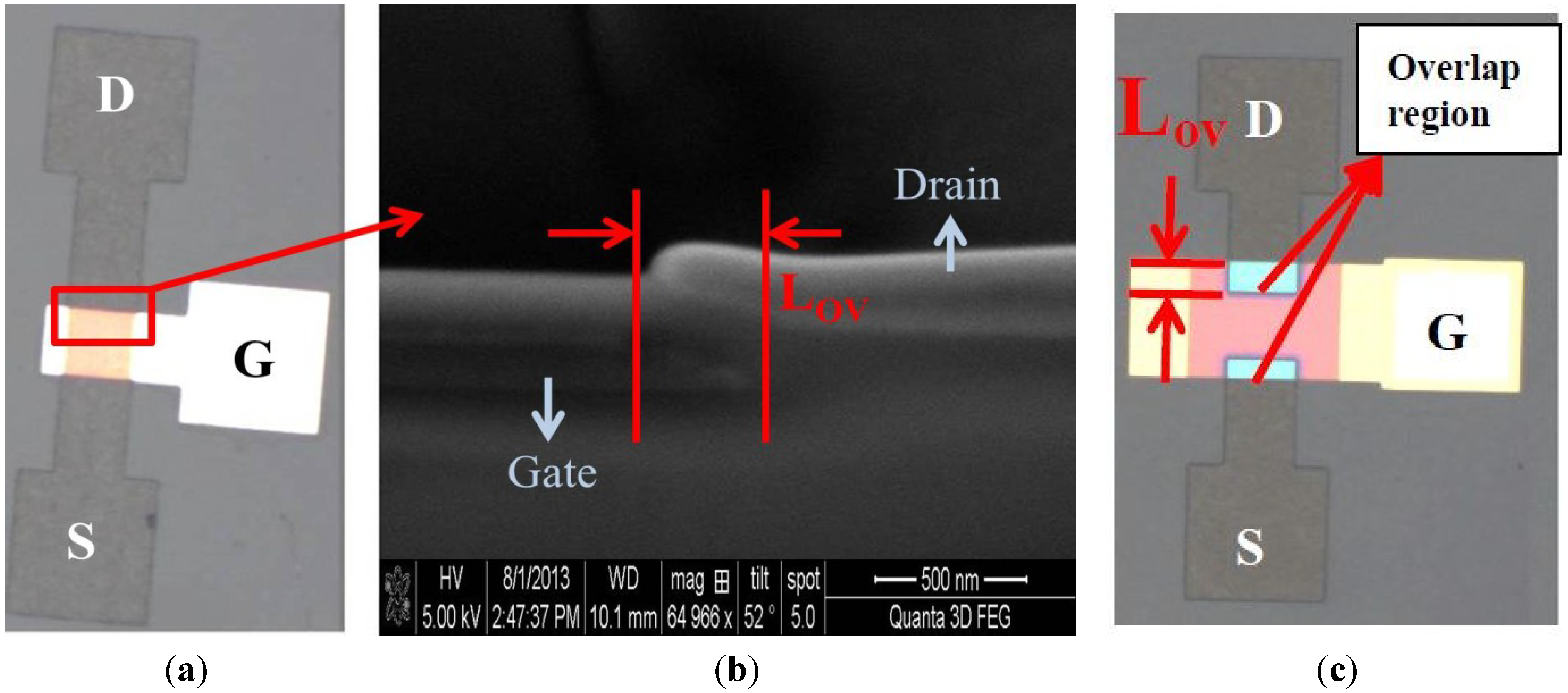
Figure 3 shows optical microscopy images and scanning electron microscopy images of the a-IGZO TFTs, which exhibit self-aligned and overlapping structures. In
Figure 3a,b, the overlapping region less than 0.5 μm could be observed in scanning electron microscopy images. The overlapping region was clearly observable among the devices fabricated using the traditional four-photo-mask process in
Figure 3c, which yielded parasitic capacitance between S/D and gate electrodes (
Cgd,
Cgs). The parasitic capacitance was proportional to the area of overlapping region (
W ×
Lov), yielding increased feed-through voltage, noise, and circuit delay in devices typically used in displays applications [
12].
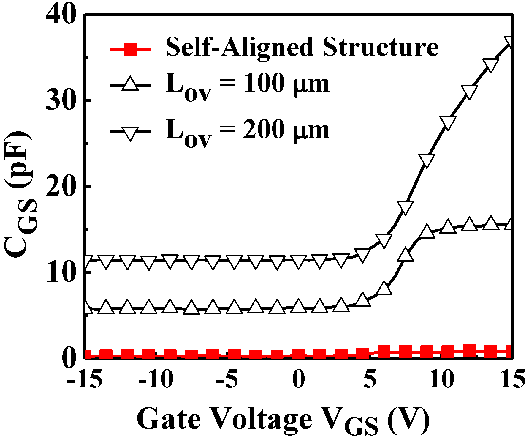
To analyze the parasitic capacitance between the S/D and gate electrodes, the capacitance–voltage of the fabricated a-IGZO TFTs was measured using an Inductance-Resistance-Capacitance (LCR) meter (HP4284A, Hewlett Packard, Palo Alto, CA, USA;
Figure 4). The capacitance markedly increased in conjunction with the overlap length (
Lov) (
i.e., the area of overlapping region). The device that was fabricated using the traditional four-photo-mask process (
i.e.,
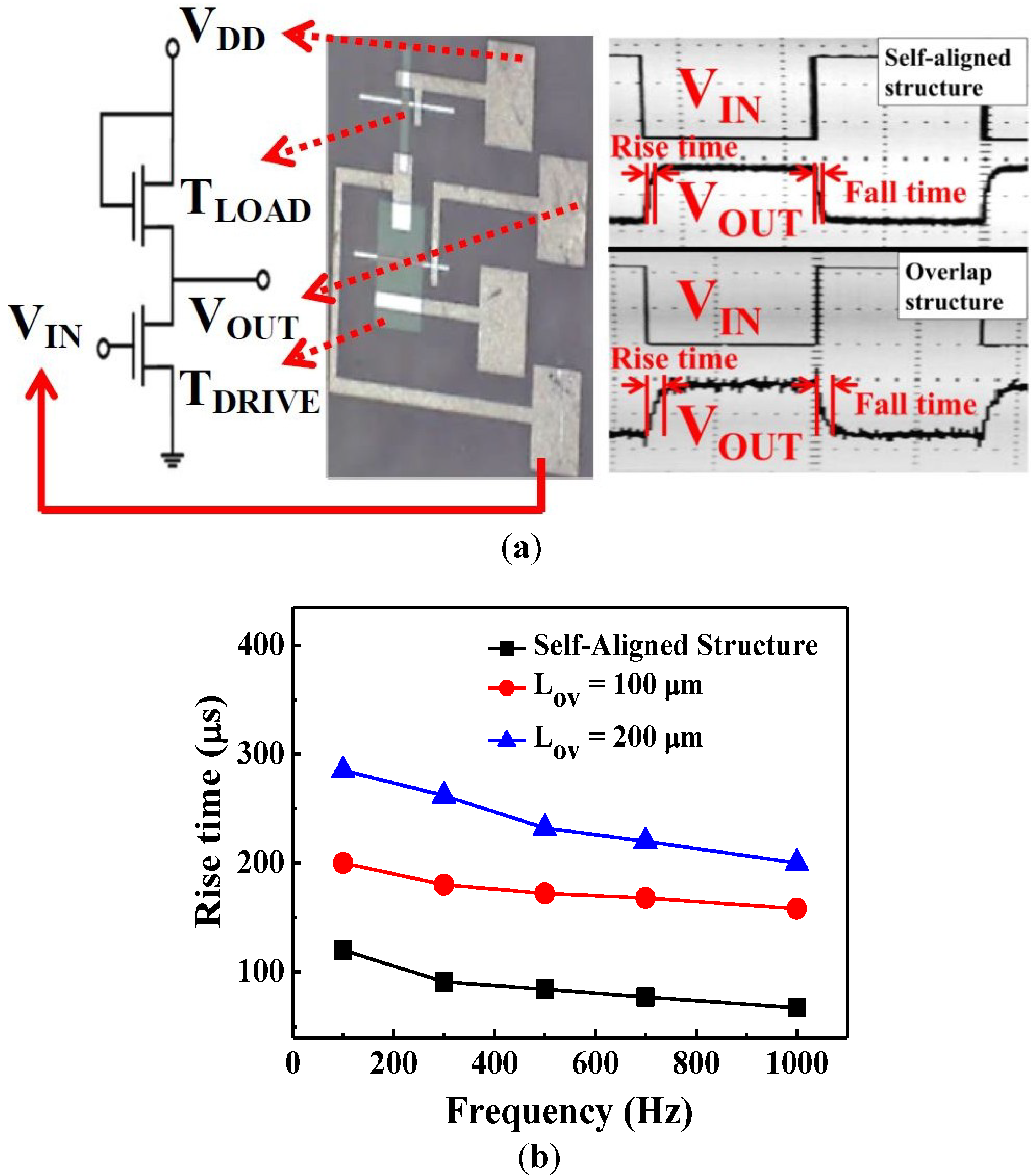
Lov of 200 μm) exhibited a minimal capacitance of 11.46 pF, which was considerably higher compared with that of the device fabricated using the proposed method (0.25 pF). Hence, the self-aligned structure reduced the parasitical capacitance between the S/D and gate electrodes. To examine the effects of parasitic capacitance, two types of the inverters were fabricated (
Figure 5a); the first comprised the proposed two-mask process with self-aligned structures, and the second comprised overlapping structures (both types employed an N-type metal-oxide-semiconductor configuration as the active load).
Figure 5a also shows the dynamic state measurements for the inverters. Various square wave frequencies (
VIN) were input into the inverters, and the output signals (
VOUT) were measured using oscilloscope. The rise time of the output signal was defined as the time required by the signal to rise from 10% to 90% of the step height; this time is related to the parasitic capacitance of TFTs due to the Resistance-Capacitance (RC) delay for inverter circuit operation.
Figure 5b indicates that the rise time (delay time) increased in conjunction with the overlap length (
Lov), (
i.e., the parasitic capacitances). Compared with inverter with
Lov of 200 μm, the inverter that comprised the proposed two-mask schemes with self-aligned structure exhibited a substantial decrease in delay time from 230 to 78 μs (the input frequency is 500 Hz).
Figure 3.
(a) Optical microscopy images of a-IGZO TFTs with self-aligned structures; (b) Scanning electron microscopy images of a-IGZO TFTs with self-aligned structures; (c) Optical microscopy images of a-IGZO TFTs with overlap structures.
Figure 3.
(a) Optical microscopy images of a-IGZO TFTs with self-aligned structures; (b) Scanning electron microscopy images of a-IGZO TFTs with self-aligned structures; (c) Optical microscopy images of a-IGZO TFTs with overlap structures.
Figure 4.
Gate-to-source capacitance (Cgs) of a-IGZO TFTs with self-aligned structure and overlap structure for different Lov (W = 200 μm).
Figure 4.
Gate-to-source capacitance (Cgs) of a-IGZO TFTs with self-aligned structure and overlap structure for different Lov (W = 200 μm).
Figure 5.
(a) Inverter composed of the fabricated a-IGZO TFTs (VDD = 20 V, WDrive = 200 μm, LDrive = 10 μm, WLoad = 40 μm, and LLoad = 10 μm); (b) The extracted rise time for inverters composed of a-IGZO TFTs with self-aligned structure and overlap structure for Lov = 100 and 200 μm.
Figure 5.
(a) Inverter composed of the fabricated a-IGZO TFTs (VDD = 20 V, WDrive = 200 μm, LDrive = 10 μm, WLoad = 40 μm, and LLoad = 10 μm); (b) The extracted rise time for inverters composed of a-IGZO TFTs with self-aligned structure and overlap structure for Lov = 100 and 200 μm.

