Crystallization of Electrodeposited Germanium Thin Film on Silicon (100)

Abstract
:1. Introduction
2. Experimental
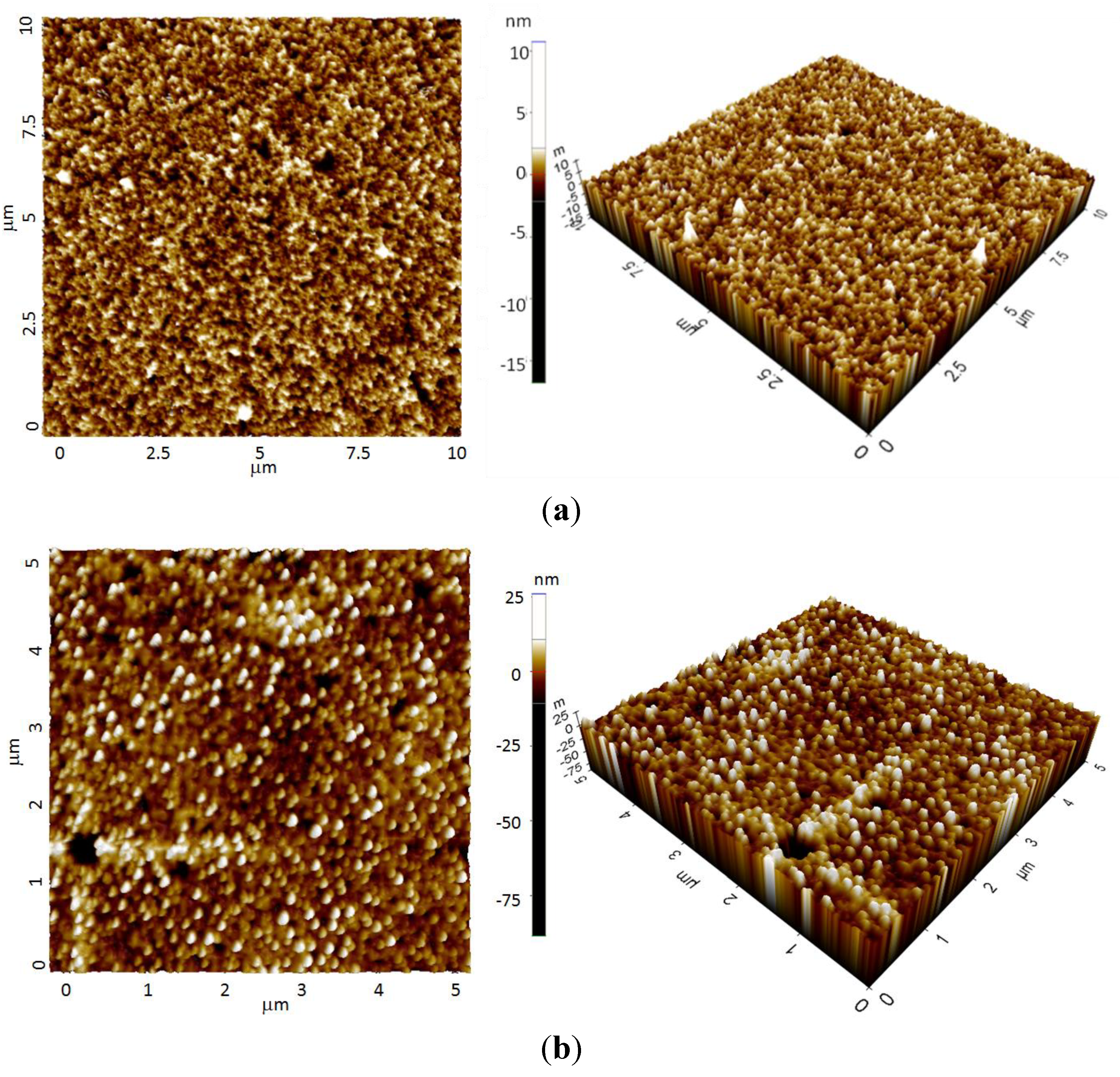
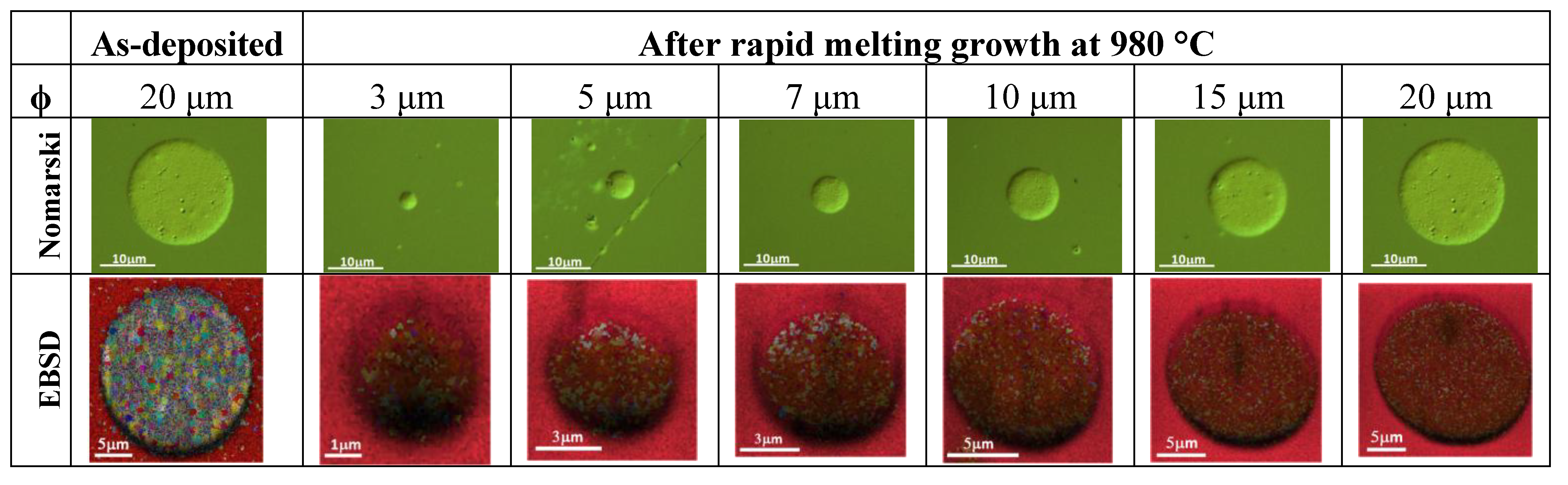
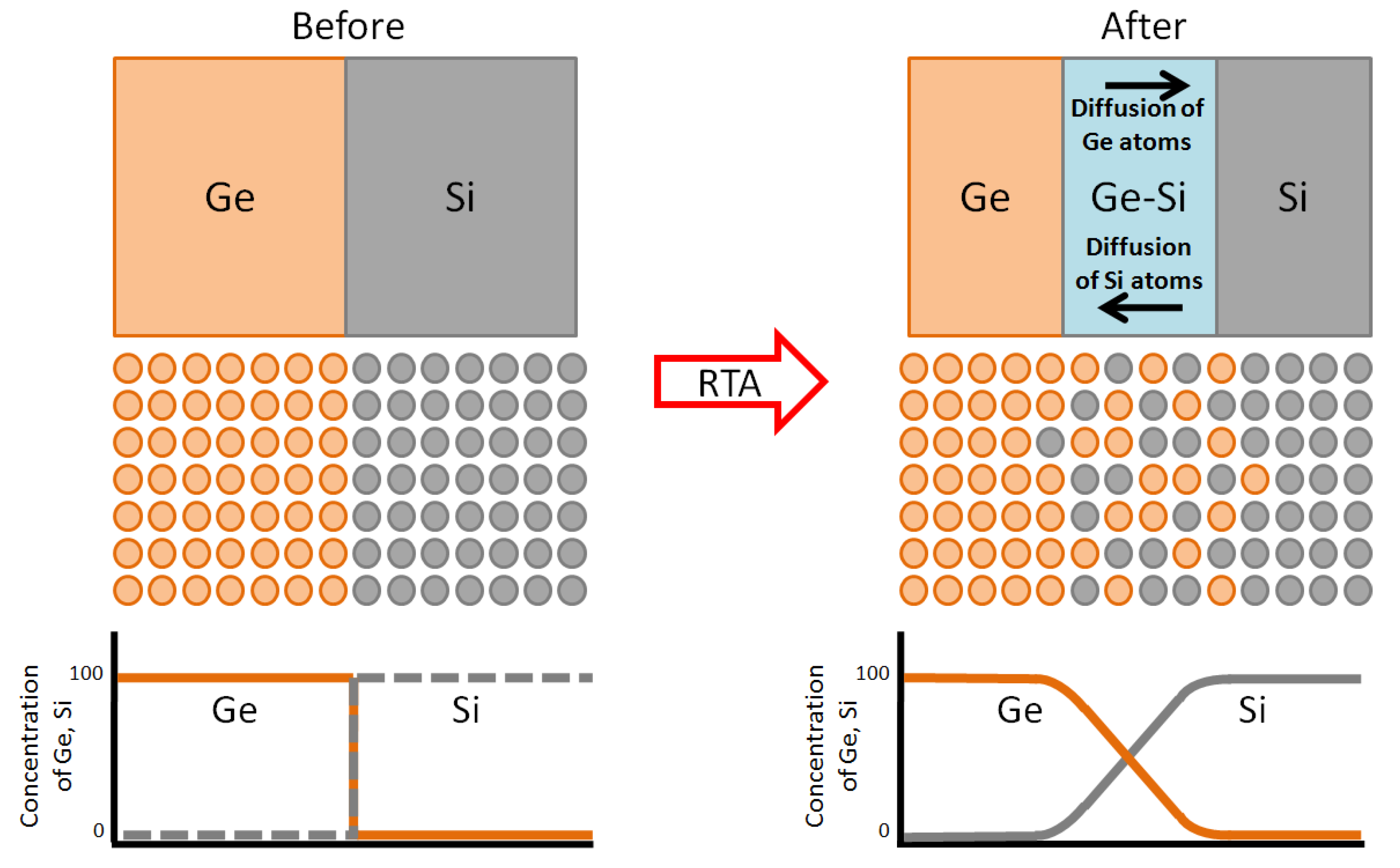
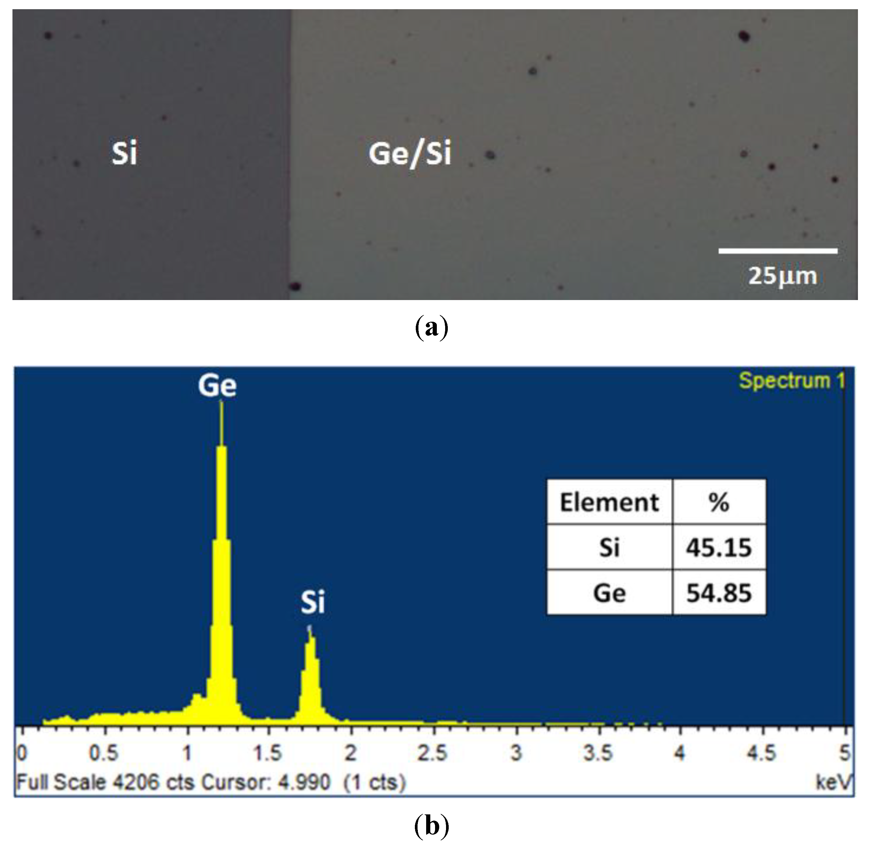
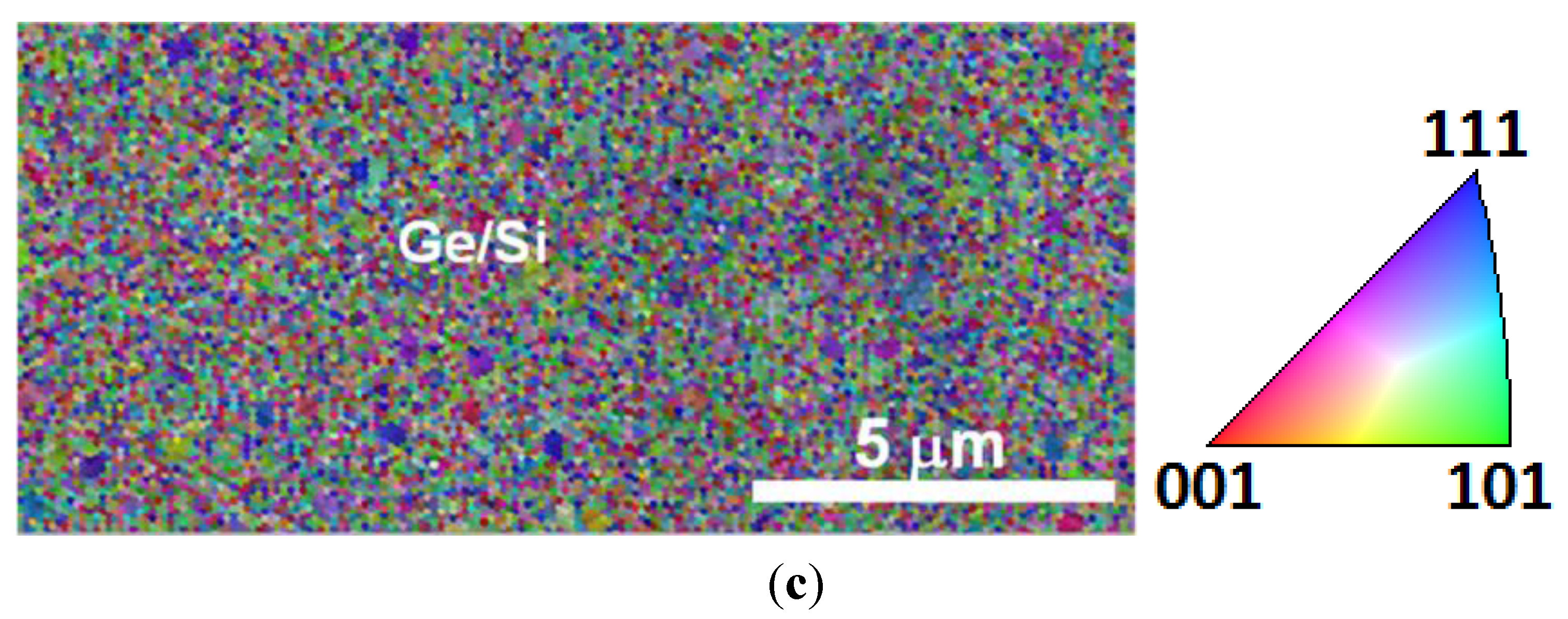
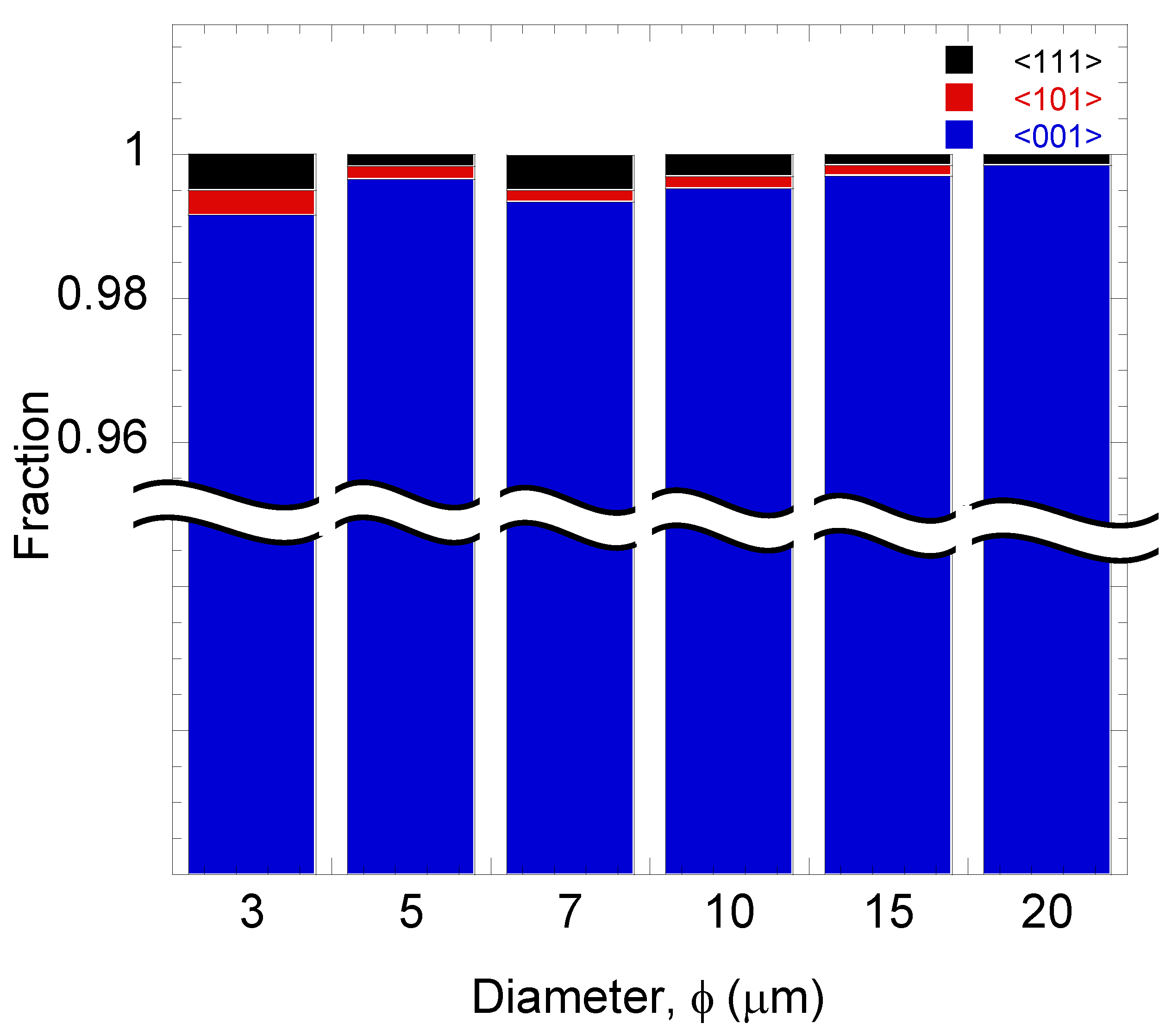
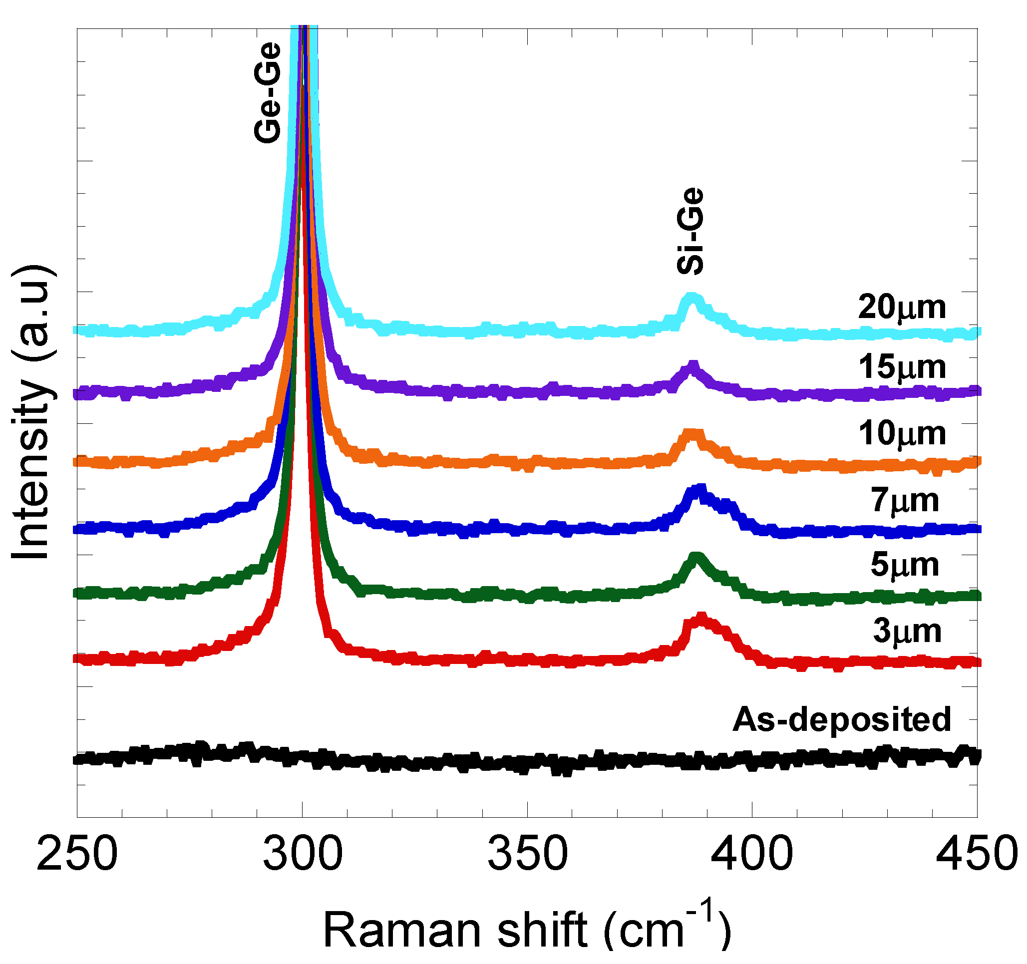
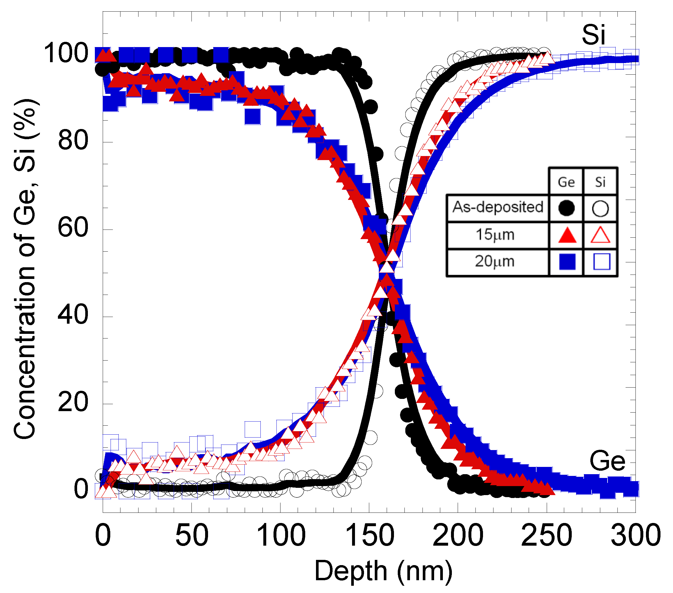
3. Results and Discussion


4. Conclusions
Acknowledgments
Conflicts of Interest
References
- International Technology Roadmap for Semiconductors. Available online: http://public.itrs.net/links/2009ITRS/Home2009.htm (accessed on 31 August 2012).
- Bescond, M.; Cavassilas, N.; Kalna, K.; Nehari, K.; Raymond, L.; Autran, J.L.; Lannoo, M.; Asenov, A. Ballistic Transport in Si, Ge and GaAs Nanowire MOSFETs. In Proceedings of Electron Devices Meeting, Washington, DC, USA, 5 December 2005; pp. 526–529.
- Takagi, S.; Sugiyama, M.; Yasuda, T.; Takenaka, M. Ge/III-V Channel Engineering for Future CMOS. In Graphene and Emerging Materials for Post-CMOS Applications; Obeng, Y., DeGendt, S., Srinivasan, P., Misra, D., Iwai, H., Karim, Z., Hess, D.W., Grebel, H., Eds.; Electrochemical Society Inc.: Pennington, Australia, 2009; pp. 9–20. [Google Scholar]
- Boucart, K.; Ionescu, A.M. Double-gate tunnel FET with high-k gate dielectric. IEEE Trans. Electron Devices 2007, 54, 1725–1733. [Google Scholar] [CrossRef]
- Liu, Y.; Gopalafishan, K.; Griffin, P.B.; Ma, K.; Deal, M.D.; Plummer, J.D. MOSFETs and High-Speed Photodetectors on Ge-on-Insulator Substrates Fabricated Using Rapid Melt Growth. In IEEE International Electron Devices Meeting, San Francisco, CA, USA, 13–15 December 2004; pp. 1001–1004.
- Abidin, M.S.Z.; Hashim, A.M.; Sharifabad, M.E.; Rahman, S.F.A.; Sadoh, T. Open-gated pH sensor fabricated on an undoped-AlGaN/GaN HEMT structure. Sensors 2011, 11, 3067–3077. [Google Scholar] [CrossRef]
- Itabashi, S.; Nishi, H.; Tsuchizawa, T.; Watanabe, T.; Shinojima, H.; Park, S.; Yamada, K.; Ishikawa, Y.; Wada, K. Integration of Optical Devices Based on Si, Ge and SiOx. In 2010 7th IEEE International Conference on Group IV Photonics (GFP), Beijing, China, 1–3 September 2010; pp. 48–50.
- Wang, J.; Lee, S. Ge-Photodetectors for Si-based optoelectronic integration. Sensors 2011, 11, 696–718. [Google Scholar] [CrossRef] [PubMed]
- Hashim, A.M.; Mustafa, F.; Rahman, S.F.A.; Rahman, A.R.A. Dual-functional on-chip AlGaAs/GaAs schottky diode for RF power detection and low-power rectenna applications. Sensors 2011, 11, 8127–8142. [Google Scholar] [CrossRef]
- Hashim, A.M.; Kasai, S.; Hasegawa, H. Observation of first and third harmonic responses in two-dimensional AlGaAs/GaAs HEMT devices due to plasma wave interaction. Superlattices Microst. 2008, 44, 754–760. [Google Scholar] [CrossRef]
- Claeys, C.; Simoen, E. Germanium-Based Technologies: From Materials to Devices; Elsevier Science: Amsterdam, The Netherlands, 2007; p. 480. [Google Scholar]
- Lokhande, C.D.; Pawar, S.H. Electrodeposition of thin film semiconductors. Phys. Status Solidi A 1989, 111, 17–40. [Google Scholar] [CrossRef]
- Jayakrishnan, S.; Pushpavanam, M.; Shenoi, B.A. Electrodeposition from organic solutions of metals that are difficult to deposit from aqueous solutions. Surf. Technol. 1981, 13, 225–240. [Google Scholar] [CrossRef]
- Endres, F.; Abedin, S.Z.E. Nanoscale electrodeposition of germanium on Au(111) from an ionic liquid: An in situ STM study of phase formation. Phys. Chem. Chem. Phys. 2002, 4, 1640–1657. [Google Scholar] [CrossRef]
- Endres, F. Ionic liquids: Promising solvents for electrochemistry. Z. Phys. Chem. 2004, 218, 255–283. [Google Scholar] [CrossRef]
- Mukhopadhyay, I.; Freyland, W. Thickness induced metal–nonmetal transition in ultrathin electrodeposited Ge films. Chem. Phys. Lett. 2003, 377, 223–228. [Google Scholar] [CrossRef]
- Szekely, G. Electrodeposition of germanium. J. Electrochem. Soc. 1951, 98, 318–324. [Google Scholar] [CrossRef]
- Szekely, G. Electroplating of Germanium. US2690422 A, 1950. [Google Scholar]
- Saitou, M.; Sakae, K.; Oshikawa, W. Evaluation of crystalline germanium thin films electrodeposited on copper substrates from propylene glycol electrolyte. Surf. Coat. Technol. 2002, 162, 101–105. [Google Scholar] [CrossRef]
- Hashim, A.M.; Anisuzzaman, M.; Muta, S.; Sadoh, T.; Miyao, M. Epitaxial-template structure utilizing Ge-on-insulator stripe arrays with nano-spacing for advanced heterogeneous integration on Si platform. Jpn. J. Appl. Phys. 2012, 51. [Google Scholar] [CrossRef]
- Liu, Y.; Deal, M.D.; Plummer, J.D. High-quality single-crystal Ge on insulator by liquid-phase epitaxy on Si substrates. Appl. Phys. Lett. 2004, 84, 2563–2565. [Google Scholar] [CrossRef]
- Tweet, D.J.; Lee, J.J.; Maa, J.-S.; Hsu, S.T. Characterization and reduction of twist in Ge on insulator produced by localized liquid phase epitaxy. Appl. Phys. Lett. 2005, 87, 141908:1–141908:3. [Google Scholar] [CrossRef]
- Gao, F.; Lee, S.J.; Balakumar, S.; Du, A.; Foo, Y.-L.; Kwong, D.-L. Ge diffusion and solid phase epitaxy growth to form Si1-x/Gex/Si and Ge on insulator structure. Thin Solid Films 2006, 504, 69–72. [Google Scholar] [CrossRef]
- Balakumar, S.; Roy, M.M.; Ramamurthy, B.; Tung, C.H.; Fei, G.; Tripathy, S.; Dongzhi, C.; Kumar, R.; Balasubramanian, N.; Kwong, D.L. Fabrication aspects of germanium on insulator from sputtered Ge on Si-substrates. Electrochem. Solid State Lett. 2006, 9, G158–G160. [Google Scholar] [CrossRef]
- Miyao, M.; Tanaka, T.; Toko, K.; Tanaka, M. Giant Ge-on-insulator formation by Si–Ge mixing-triggered liquid-phase epitaxy. Appl. Phys. Express 2009, 2. [Google Scholar] [CrossRef]
- Toko, K.; Sakane, T.; Tanaka, T.; Sadoh, T.; Miyao, M. Defect-free single-crystal Ge island arrays on insulator by rapid-melting-growth combined with seed-positioning technique. Appl. Phys. Lett. 2009, 95, 112107:1–112107:3. [Google Scholar] [CrossRef]
- Huang, Q.; Bedell, S.W.; Saenger, K.L.; Copel, M.; Deligianni, H.; Romankiwa, L.T. Single-crystalline germanium thin films by electrodeposition and solid-phase epitaxy. Electrochem. Solid State Lett. 2007, 10, D124–D126. [Google Scholar] [CrossRef]
- Mooney, P.M.; Dacol, F.H.; Tsang, J.C.; Chu, J.O. Raman scattering analysis of relaxed GexSi1−x alloy layers. Appl. Phys. Lett. 1993, 62, 2069–2071. [Google Scholar] [CrossRef]
- Olesinski, R.W.; Abbaschian, G.J. The Ge-Si (Germanium-Silicon) system. Bull. Alloy Phase Diagr. 1984, 5, 180–183. [Google Scholar] [CrossRef]
- Strain Measurements of a Si Cap Layer Deposited on a SiGe Substrate Determination of Ge Content. Available online: http://www.intercovamex.com/biblioteca_de_aplicaciones/SEMICONDUCTORES/Mediciones%20de%20tension%20de%20de%20una%20capa%20de%20Si%20depositada%20en%20un%20sustrato%20de%20SiGe.%20Determinacion%20del%20contenido%20de%20Ge.pdf (accessed on 9 June 2012).
© 2013 by the authors; licensee MDPI, Basel, Switzerland. This article is an open access article distributed under the terms and conditions of the Creative Commons Attribution license (http://creativecommons.org/licenses/by/3.0/).
Share and Cite
Abidin, M.S.Z.; Matsumura, R.; Anisuzzaman, M.; Park, J.-H.; Muta, S.; Mahmood, M.R.; Sadoh, T.; Hashim, A.M. Crystallization of Electrodeposited Germanium Thin Film on Silicon (100). Materials 2013, 6, 5047-5057. https://doi.org/10.3390/ma6115047
Abidin MSZ, Matsumura R, Anisuzzaman M, Park J-H, Muta S, Mahmood MR, Sadoh T, Hashim AM. Crystallization of Electrodeposited Germanium Thin Film on Silicon (100). Materials. 2013; 6(11):5047-5057. https://doi.org/10.3390/ma6115047
Chicago/Turabian StyleAbidin, Mastura Shafinaz Zainal, Ryo Matsumura, Mohammad Anisuzzaman, Jong-Hyeok Park, Shunpei Muta, Mohamad Rusop Mahmood, Taizoh Sadoh, and Abdul Manaf Hashim. 2013. "Crystallization of Electrodeposited Germanium Thin Film on Silicon (100)" Materials 6, no. 11: 5047-5057. https://doi.org/10.3390/ma6115047
APA StyleAbidin, M. S. Z., Matsumura, R., Anisuzzaman, M., Park, J.-H., Muta, S., Mahmood, M. R., Sadoh, T., & Hashim, A. M. (2013). Crystallization of Electrodeposited Germanium Thin Film on Silicon (100). Materials, 6(11), 5047-5057. https://doi.org/10.3390/ma6115047