Communication

The Mechanism of Ruthenium Oxide Catalyzed Electroless Etching of Silicon in Oxidizing HF Solution

Key Laboratory of Multiscale Spin Physics, Ministry of Education, Beijing Key Laboratory of Energy Conversion and Storage Materials, School of Physics and Astronomy, Beijing Normal University, Beijing 100875, China
*
Author to whom correspondence should be addressed.
Materials 2026, 19(9), 1734; https://doi.org/10.3390/ma19091734
Submission received: 24 March 2026 / Revised: 22 April 2026 / Accepted: 23 April 2026 / Published: 24 April 2026
(This article belongs to the Section Catalytic Materials)

Abstract

While metal-assisted chemical etching (MACE) or metal-catalyzed electroless etching of silicon in oxidizing HF solutions typically employs noble metals as catalysts, this work investigates oxide-catalyzed chemical etching (OACE) using RuO2 to induce localized silicon etching in aqueous H2O2-HF solutions. RuO2 particles confine the reaction to localized sites. The formation of Ru2O3 during etching suggests that RuO2 injects holes into silicon and is simultaneously reduced to Ru2O3. The oxidized silicon is locally dissolved in aqueous HF solution, and the pores are generated. A cyclic redox mechanism is proposed: RuO2 is reduced to Ru2O3 by extracting electrons from silicon valence band, while Ru2O3 is rapidly reoxidized by H2O2, sustaining the etching process until H2O2 is exhausted. This work challenges the conventional assumption that the catalyst remains unchanged during MACE and offers novel insights into oxide-catalyzed silicon etching mechanisms.

1. Introduction

Metal-assisted chemical etching (MACE) is a simple, controllable and cost-effective approach for fabricating a wide range of silicon micro- and nanostructures [1,2,3,4,5,6,7,8]. This method relies on metal catalysts (e.g., Au, Ag, Pt) to induce localized electrochemical reactions during wet etching in HF solutions, enabling selective etching of silicon with nanoscale control over corrosion morphology [9,10,11,12,13]. As demonstrated in previous studies, various desired silicon micro/nanostructures can be obtained by tailoring the catalyst type and morphology, adjusting the composition or concentration of the etchant, modifying the doping type and level of the silicon substrate, or applying additional physical fields (e.g., an external electric field or irradiation) during etching in HF solution [14,15,16,17,18,19,20,21]. From a chemical perspective, an effective MACE should: (i) efficiently catalyze the relevant electrochemical reactions; (ii) exhibit an electronegativity greater than that of silicon; and (iii) be capable of injecting holes into the valence band of silicon, either intrinsically or upon oxidation; in other words, possess a high redox potential [21,22,23,24,25,26,27,28]. Gayrard et al. [29] proposed replacing noble metals with transition metal oxides for this purpose, a process termed oxide-assisted chemical etching (OACE). They suggested that transition metal oxides such as RuO2 and IrO2 exhibit catalytic properties comparable to those of noble metals. By depositing nanopatterned films of RuO2 and IrO2 on silicon surfaces and etching in a mixed solution of hydrogen peroxide and hydrofluoric acid, they successfully prepared vertically aligned silicon nanowire arrays. Analogous to metal-catalyzed etching, they attributed this phenomenon to the catalytic injection of holes from hydrogen peroxide into silicon by the metal oxides, thereby inducing the silicon etching reaction. However, although ruthenium oxides are highly effective catalysts for the oxygen evolution reaction (OER), they suffer from limited stability in acidic media [30,31,32,33], and dissolution or corrosion of ruthenium oxides may occur.
In this work, we deposited synthesized RuO2 onto silicon surfaces and immersed the samples in a mixed solution of hydrofluoric acid and hydrogen peroxide. During silicon etching, the formation of Ru2O3 was observed. We propose that RuO2 injects holes into silicon and is reduced to Ru2O3, which is subsequently oxidized to RuO2 by hydrogen peroxide. This cycle continues until the hydrogen peroxide in the solution is depleted, at which point the silicon etching ceases. This finding challenges the conventional view that the catalyst is not directly involved in the etching reaction in traditional MACE/OACE models, revealing that transition metal oxides can act as a dynamic ‘hole pump’ during etching, rather than merely serving as an electron transfer medium. Compared with previous studies, we report for the first time the valence state change in RuO2 during silicon etching and its synergistic cyclic reaction with silicon and H2O2.

2. Materials and Methods

2.1. Materials

One-side polished single crystalline (100)-oriented p-Si wafers (B-doped, ρ = 15–25 Ω·cm) were used in the experiment and purchased from Beijing General Research Institute (Beijing, China) for Non-Ferrous Metals. Ruthenium (III) chloride trihydrate (RuCl3·3H2O), Hydrogen peroxide (H2O2), Hydrofluoric acid (HF), sodium hydroxide (NaOH), etc., were purchased from Aladdin Chemical Reagent Co., Ltd., Shanghai (China).

2.2. Sample Preparation

Silicon wafers were cleaved into 2 × 2 cm2 samples. The cleaved Si wafer pieces were first ultrasonically cleaned in acetone and ethanol for 10 min, respectively, subsequently immersed in a boiling H2SO4 and H2O2 (PIRANHA) solution for 30 min. After each cleaning step, the Si pieces were thoroughly rinsed with deionized (DI) water and followed by drying in flowing N2.
Synthesis of RuO2-1. 0.126 g of RuCl3·3H2O was dissolved in 100 mL of DI water to prepare a RuCl3 solution. Separately, 0.2 g of NaOH was dissolved in 100 mL of DI water to obtain a 0.05 mol/L NaOH solution. Under continuous stirring, the NaOH solution was slowly added dropwise to the RuCl3 solution at 30 °C in a water bath until the pH reached 7. The resulting precipitate was collected via vacuum filtration, washed three times with DI water to remove residual ions, and dried in an oven at 60 °C for 12 h. The dried product was ground in an agate mortar and annealed in a tube furnace at 500 °C under a flowing N2 atmosphere for 5 h to yield the final RuO2-1 sample.
Synthesis of RuO2-2. 0.5 g of RuCl3·3H2O was dissolved in 25 mL of DI water. The solution was sonicated for 30 min and then magnetically stirred for 3 h. The mixture was transferred to a Teflon-lined autoclave and subjected to hydrothermal treatment at 120 °C for 12 h. After cooling, the product was separated by centrifugation and washed three times with DI water, then dried at 80 °C for 72–96 h. The dried material was annealed in a tube furnace at 500 °C under a N2 atmosphere for 5 h to obtain the RuO2-2 sample.
RuO2-catalyzed corrosion of silicon. The as-synthesized RuO2 particles were uniformly dispersed onto the surface of a silicon wafer piece. To prevent particle displacement during etching, the coated wafer was covered with another clean silicon wafer of the same size. The stacked wafers were immersed in a H2O2-HF solution for etching. After etching, the wafer piece was rinsed with DI water and dried with N2 gas.

2.3. Characterization and Electrochemical Measurements

The morphology of etched silicon surface was examined using scanning electron microscopy (SEM, Gemini 300, ZEISS, Oberkochen, Germany). The chemical states of Ru species were analyzed by X-ray photoelectron spectroscopy (XPS, ESCALAB 250Xi, Thermo Fisher Scientific, Waltham, MA, USA) with an Al Kα X-ray source. The crystal structure was characterized by X-ray diffraction (XRD, D8 Advance, Bruker, Karlsruhe, Germany) with Cu-Κα radiation. The cathodic current density during the corrosion process was measured using a Zennium electrochemical workstation (IM6, Zahner, Kronach, Germany). Elemental composition was analyzed by energy-dispersive X-ray spectroscopy (EDS, Ultim MAX, Oxford, UK).

3. Results and Discussion

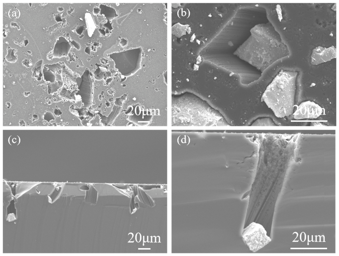
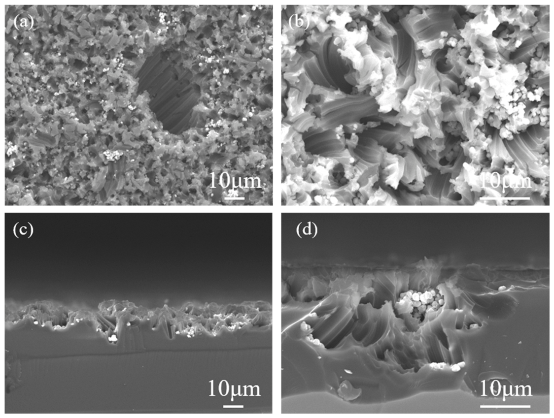
Figure 1 shows the characterization of RuO2-1 and RuO2-2 particles prepared via Synthesis 1 and Synthesis 2, respectively. Figure 2 presents top-view and cross-sectional SEM images of a RuO2-1-coated single-crystalline Si (100) wafer after 1 h of etching in a HF-H2O2 solution. The top-view images (Figure 2a,b) show that etching occurred exclusively at RuO2 particle sites, with pore geometries faithfully replicating the irregular morphology of the catalyst particles. Regions without RuO2 remained unetched, confirming that RuO2 is essential for initiating corrosion. Smaller particles generated shallow pores, whereas larger ones produced deeper pores. High-magnification SEM (Figure 2b) reveals uneven pore walls, which can be attributed to the rough surface topography of RuO2-1 that embeds into the Si substrate and induces localized etching. Cross-sectional analysis (Figure 2c,d) further demonstrates that the etching depth is positively correlated with the particle size. The larger the particle, the greater the corresponding etching depth, whereas smaller particles remain confined near the surface region.
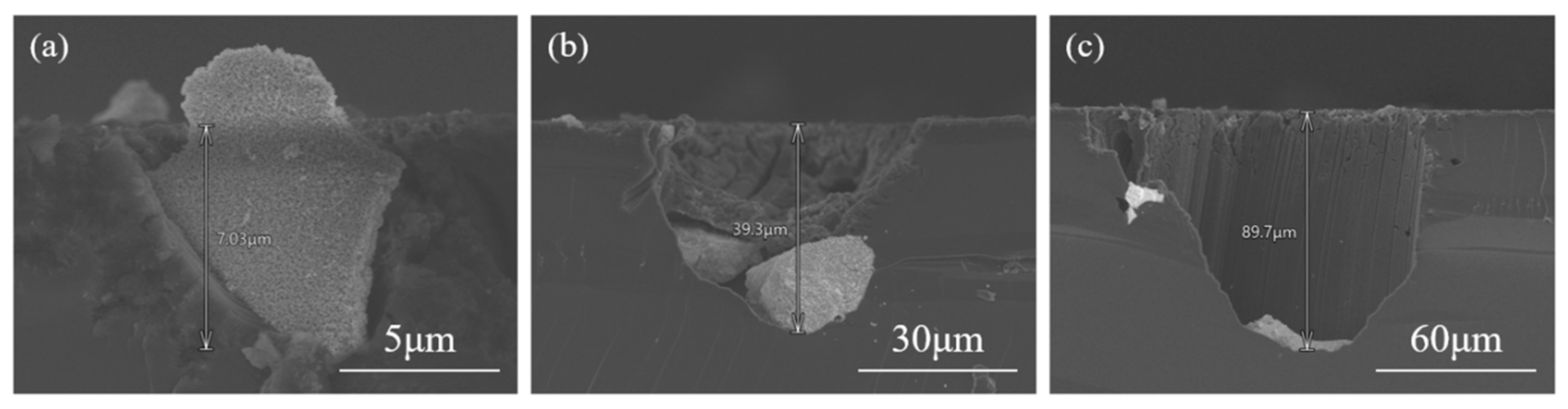
As the RuO2 particle size increases from approximately 5 μm to 30 μm and further to 60 μm, the etching depth correspondingly increases from 7.03 μm to 39.3 μm and further to 89.7 μm (Figure 3). The size-dependent behavior suggests that more holes are generated in the vicinity of large particles. Notably, the pore diameters near the Si surface were larger than those at the etching front (Figure 2d).
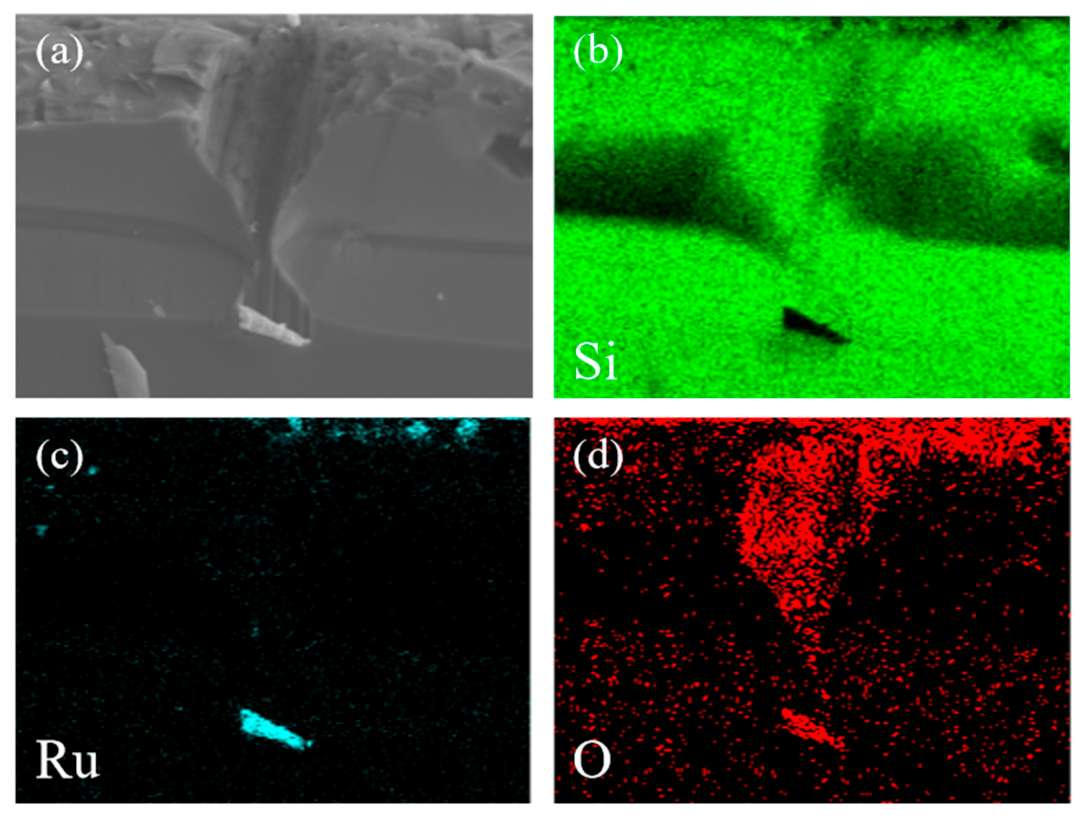
The EDS elemental mapping (Figure 4) clearly shows that selective etching of the Si substrate occurs exclusively at sites where RuO2 particles are present. In contrast, regions without RuO2 remain unetched, confirming that the localized etching behavior is directly induced by the RuO2 catalyst.
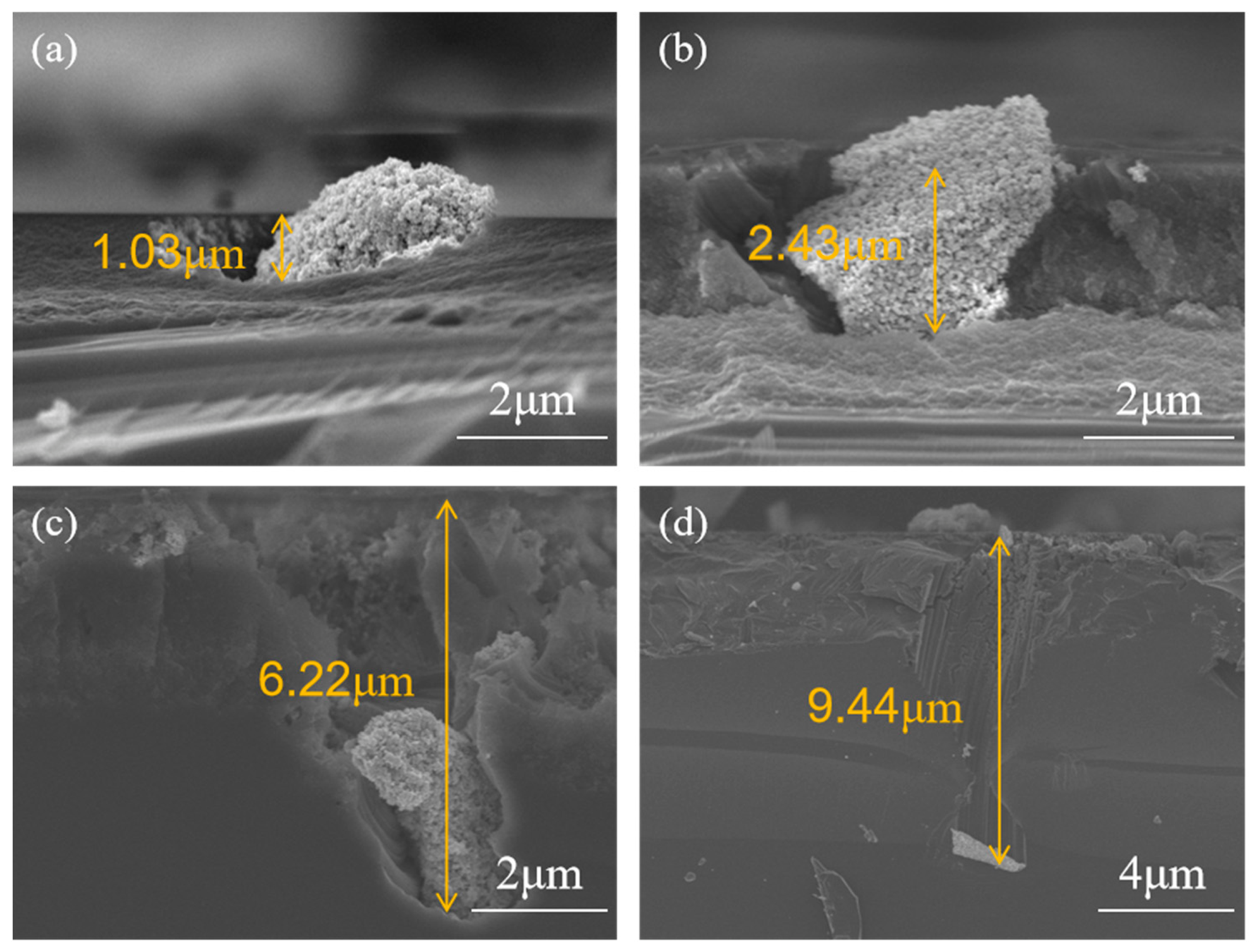
A quantitative analysis of pore depth with the etching time (Figure 5) was performed using RuO2 particles with a diameter of approximately 2 µm. The results show that the etching depth increases with time, reaching 1.03 µm, 2.43 µm, 6.22 µm, and 9.44 µm at 10 min, 30 min, 1 h, and 2 h, respectively. Notably, the evolution of etching depth does not follow a linear relationship with time, indicating a time-dependent decrease in the etching rate. This behavior suggests that the process is kinetically controlled, where the gradual depletion of H2O2, leads to a progressive deceleration of the etching kinetics.
Figure 6 illustrates the etching behavior of RuO2-2-coated Si under identical conditions. Similarly, etching occurs only at sites where RuO2-2 particles were present. The spherical RuO2-2 particles (Figure 6a,b) induced disordered surface etching with tilted or rotated pores. This phenomenon arises from the mobility and aggregation of small particles in solution, as evidenced by clustered RuO2-2 particles (Figure 6b). Cross-sectional SEM (Figure 6c,d) reveals pore depths of 10–30 µm. At sites with fewer RuO2-2 particles, the catalytic activity was weaker and the etching reaction proceeded more slowly. Excessive accumulation of RuO2-2 particle hindered the access of the solution to the reaction interface, suppressing the oxidation and dissolution of silicon and resulting in relatively shallow etching depths. Therefore, the density of RuO2-2 particles on the silicon surface plays a critical role in the etching process. The etching behavior of Si is known to be crystallographically anisotropic, with etching rates varying across different orientations due to differences in surface bond density and reactivity. According to the principle of minimum energy, preferential etching is expected to proceed along the <100> direction. However, our observations suggest that the mobility of RuO2 particles during the etching process introduces additional complexity. For isolated or sparsely distributed RuO2 particles, the etching direction can change dynamically, following the moving trajectory of the catalyst particles. In contrast, in regions where RuO2 particles are aggregated, their mobility is spatially constrained, and the etching proceeds predominantly along the <100> direction. Therefore, the final pore morphology is determined by the interplay between Si crystallographic anisotropy and the local distribution and mobility of the RuO2 catalyst.
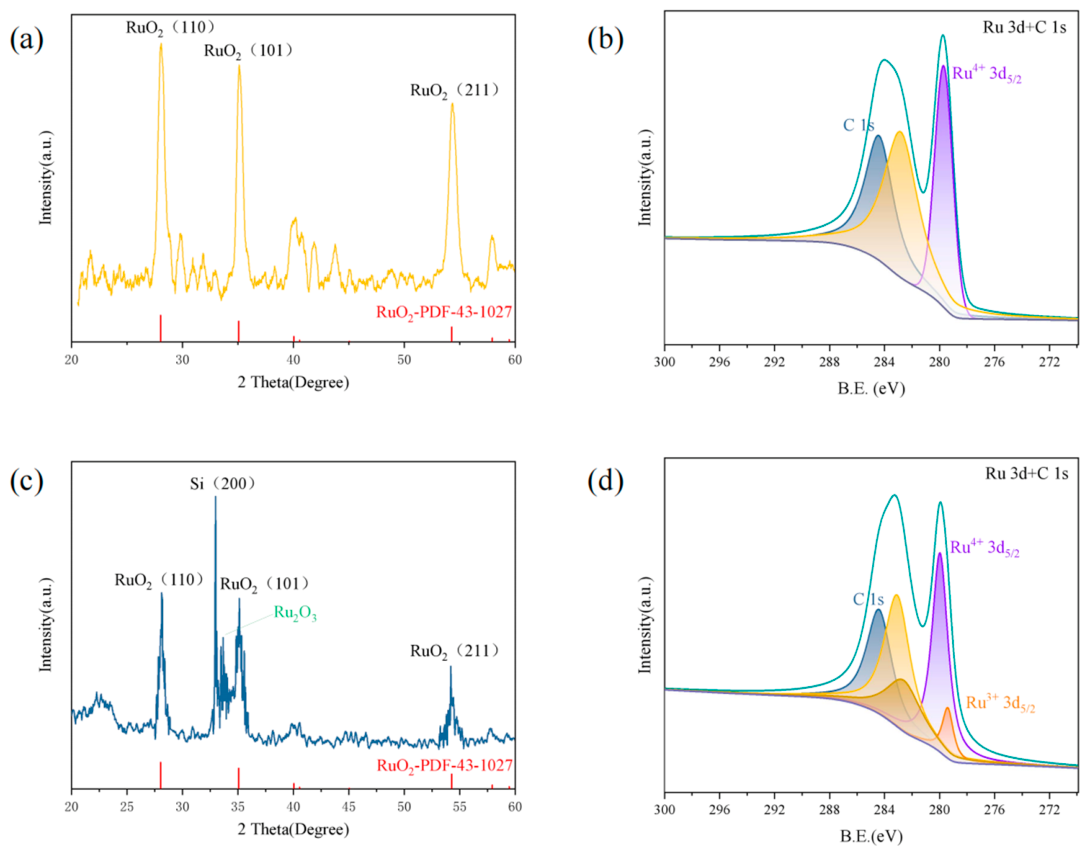
To determine whether the catalyst undergoes chemical transformation during etching, RuO2 before and after catalyzing the silicon etching were analyzed by XRD (Figure 7a,c) and XPS (Figure 7b,d). The characteristic peaks at 28.08°, 35.10°, and 54.32°, corresponding to (110), (101), and (211) crystal planes of rutile RuO2, respectively, are consistent with the RuO2 phase (JCPDS #43-1027) [33]. The XRD patterns of etched silicon wafers coated with RuO2 exhibit two additional peaks besides the characteristic peaks of RuO2. The characteristic peaks at 32.98° and 33.66° correspond to the (200) crystal plane of single-crystal silicon and the characteristic peak of Ru2O3, respectively, indicating the formation of Ru2O3. To ensure reliable phase identification, the standard peak positions of Ru2O3 [30,34] are provided in the Supporting Information (Figure S1) for direct comparison with the experimental XRD pattern. Figure 7b,d show the XPS spectra in the Ru 3d region. The Ru 3d core-level spectrum was deconvoluted using a mixed Gaussian-Lorentzian function after Shirley background subtraction. Before catalyzing the etching of silicon, only one Ru 3d spin–orbit doublet was observed. The component at 279.9 eV (Ru 3d5/2) is attributed to Ru4+, which is consistent with the peak position of RuO2 (280.3 eV) [35]. The slight shift in the peak position can be ascribed to the RuO2 particles being in an electron-rich state. The Ru3+ 3d5/2 peak is identified at 279.1 eV, which is exactly 0.8 eV lower than the Ru4+ peak. This separation is highly consistent with the work of Sayan et al. [36], where the Ru3+ 3d5/2 peak is typically found approximately 0.8 eV below that of Ru4+.
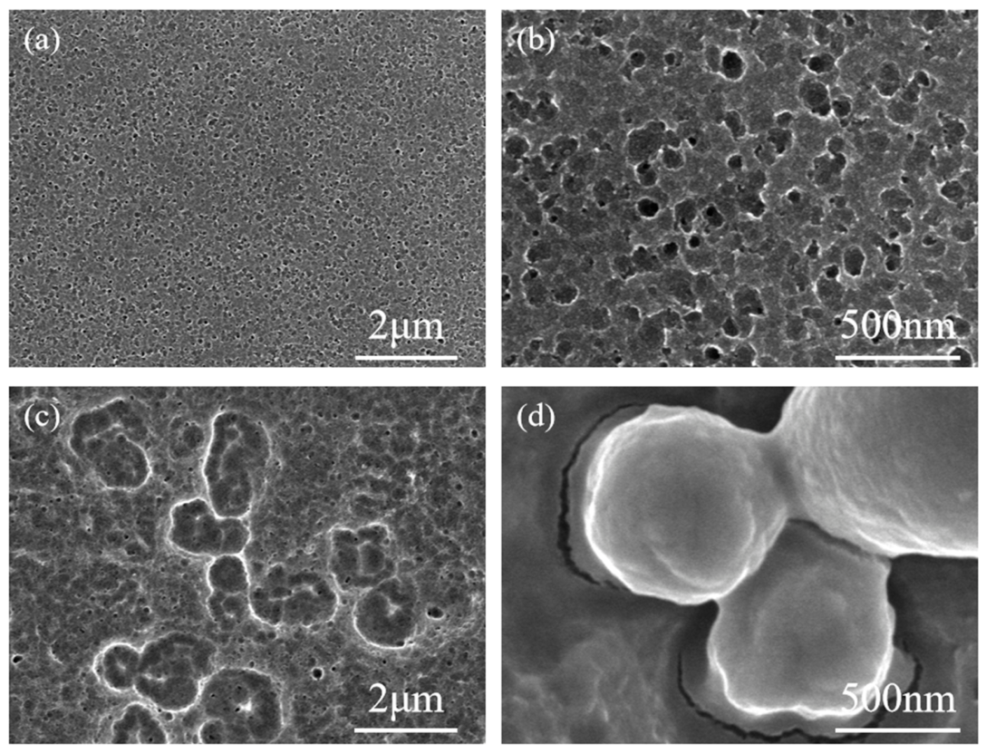
To further investigate the role of the oxidant in the etching process, we replaced H2O2 with O2 and compared the resulting etching behavior. The RuO2-coated silicon wafers were transferred into a PTFE reactor containing aerated HF/H2O vapor. Figure 8 shows the SEM images of wafers etched in aerated HF/H2O vapor at 295 K for different durations. After 5 h, only a porous layer formed on the surface, with no evidence of deep pore propagation. When the etching time was extended to 22 h, RuO2 particles remained embedded on the silicon surface without further downward etching. In contrast, deep pores (up to 60 μm) were readily formed within 1 h (Figure 2) when H2O2 was used as the oxidant.
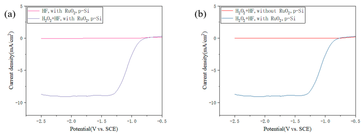
The oxidation of Ru2O3 to RuO2 by H2O2 (Reaction (2)) is known to be both thermodynamically favorable and kinetically fast under acidic conditions, as H2O2 is a strong two-electron oxidant with a standard reduction potential of +1.78 V (H2O2 + 2H+ + 2e → 2H2O). However, the oxidation of Ru2O3 by molecular oxygen (O2 + 4H+ + 4e → 2H2O, E° = +1.23 V) is thermodynamically less favorable and, more importantly, exhibits extremely slow kinetics at room temperature. In the dark state, the magnitude of the cathodic polarization current reflects the strength of hole injection. The greater the polarization current, the stronger the ability to inject holes into the valence band of silicon. We compared the cathodic polarization curves of RuO2-plated silicon wafers in HF solution with H2O2 or dissolved O2 (Figure 9a). The polarization current of the RuO2-plated silicon wafer in HF solution with dissolved O2 was an order of magnitude smaller than that of the RuO2-plated silicon wafer in HF-H2O2 solution. While RuO2 can still inject holes into silicon and be reduced to Ru2O3 at the Si/RuO2 interface, the reoxidation of Ru2O3 back to RuO2 by O2 is inefficient. The accumulation of Ru2O3 at the interface rapidly suppresses further hole injection, leading to a self-limiting behavior in which only shallow surface etching occurs and small cathode current is observed. In contrast, H2O2 can efficiently reoxidize Ru2O3 to RuO2, sustaining the cyclic redox process and hole injection into the valence band of silicon, resulting in the generation of a large cathodic current and continuous deep pore formation. The dark cathodic polarization current of the RuO2-plated silicon wafer was significantly greater than that of the pure silicon wafer in HF-H2O2 solution (Figure 9b), indicating that the presence of RuO2 greatly enhances the ability of hole injection.
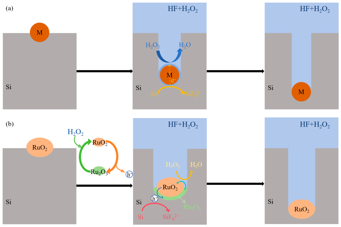
The schematic illustration of the MACE mechanism is shown in Figure 10a. In conventional MACE, the noble metal catalyst (such as Au, Ag, or Pt) remains chemically unchanged throughout the etching process. It serves as a cathodic site that confines the etching reaction to localized sites, attracting electrons from silicon. The oxidant (such as H2O2) extracts electrons from silicon at the metal particle surface and injects holes into silicon, thereby enabling rapid etching [26,27,28]. In the RuO2-catalyzed silicon etching process, we suggest that RuO2 particles serve two functions in catalyzing silicon etching: (1) confining the silicon etching reaction to the Si/ RuO2 interface, and (2) injecting holes into the valence band of silicon to initiate oxidation. A schematic illustration of the RuO2-catalyzed silicon etching mechanism is shown in Figure 10b. At the Si/ RuO2 interface, RuO2 particles in contact with silicon are reduced to Ru2O3 by extracting electrons from the silicon valence band, as described by Reaction (1). Since the etchant contains H2O2, a strong oxidizing agent, Ru2O3 is rapidly oxidized by H2O2 back to RuO2 via Reaction (2). It should be noted that ruthenium species predominantly exist as RuO2 throughout the process, with the generated intermediate species (Ru2O3) being transient and localized around the RuO2 particles. The ruthenium species undergo the cyclic redox process until the hydrogen peroxide is exhausted. Substantial holes accumulate at the Si/ RuO2 interface, initiating anodic oxidation of silicon through both four-electron (Reactions (3) and (4)) and two-electron (Reaction (5)) pathways. This electrochemical process generates hydrogen gas and yields water-soluble hexafluorosilicic acid (H2SiF6) as the primary reaction product. The overall reaction related to silicon can be comprehensively described by Reaction (6). Table 1 shows a comparison between MACE and OACE in terms of charge transfer, catalyst behavior, and reaction pathways.
2 Ru O 2 + 2 H + + 2 e Ru 2 O 3 +   H 2 O       E = 0.973 V
Ru 2 O 3 +   H 2 O 2 2 Ru O 2 + H 2 O
Si + 2 H 2 O + 4 h + Si O 2 + 4 H +       E = 0.84 V
Si O 2 + 6 HF H 2 Si F 6 + 2 H 2 O
Si + 6 F + 2 H + + 2 h + Si F 6 2 + H 2       E = 1.2 V
Si + 6 HF + n 2 H 2 O 2 H 2 Si F 6 + n H 2 O + 4 n 2 H 2  

4. Conclusions

In summary, this work elucidates the fundamental mechanism of oxide-catalyzed silicon etching in oxidizing HF solutions. Morphological characterization and compositional analysis demonstrated that Ru2O3 is generated during the etching process of RuO2-coated silicon in HF-H2O2 solutions. RuO2 injects holes into the valence band of silicon, thereby initiating silicon oxidation. Hydrogen peroxide serves to oxidize Ru2O3, sustaining the oxidation reaction of silicon. The ruthenium species undergo a cyclic process involving reduction of RuO2 to Ru2O3 and subsequent reoxidation to RuO2 by H2O2. The oxidized silicon is dissolved by hydrofluoric acid, ultimately resulting in the formation of deep pores. The proposed mechanism provides a complementary perspective to the existing models of OACE.

Supplementary Materials

The following supporting information can be downloaded at: https://www.mdpi.com/article/10.3390/ma19091734/s1, Figure S1: XRD patterns of Ru2O3 and RuO2.

Author Contributions

Conceptualization, B.B., W.X. and Y.L.; Methodology, B.B., J.L. and Y.L.; Software, W.X. and J.W.; Formal analysis, B.B., P.L. and J.L.; Investigation, B.B., P.L., J.L. and W.X.; Resources, Y.L. and J.W.; Data curation, W.X. and Y.L.; Writing—original draft, B.B.; Writing—review and editing, K.-Q.P.; Supervision, K.-Q.P.; Project administration, K.-Q.P.; Funding acquisition, K.-Q.P. All authors have read and agreed to the published version of the manuscript.

Funding

The authors gratefully acknowledge the financial support from the National Natural Science Foundation of China (52371210), Major Project of Guangzhou National Laboratory Grant No. GZNL2024A01028, and the State Key Laboratory of Catalysis (E404082900).

Data Availability Statement

The original contributions presented in this study are included in the article/Supplementary Materials. Further inquiries can be directed to the corresponding author.

Conflicts of Interest

The authors declare no conflicts of interest.

References

  1. Shim, B.; Park, K.-R.; Kim, H.; Kim, C.; Song, Y.; Kim, W.-B. Scalable fabrication of ultra-long silicon nanowires via H2O2-enhanced MACE for flexible hydrogen sensors. Chem. Eng. J. 2025, 520, 165632. [Google Scholar] [CrossRef]
  2. Surdo, S.; Barillaro, G. Voltage-and Metal-assisted Chemical Etching of Micro and Nano Structures in Silicon: A Comprehensive Review. Small 2024, 20, e2400499. [Google Scholar] [CrossRef]
  3. Huo, C.; Wang, J.; Fu, H.; Li, X.; Yang, Y.; Wang, H.; Mateen, A.; Farid, G.; Peng, K.Q. Metal-Assisted Chemical Etching of Silicon in Oxidizing HF Solutions: Origin, Mechanism, Development, and Black Silicon Solar Cell Application. Adv. Funct. Mater. 2020, 30, 2005744. [Google Scholar] [CrossRef]
  4. Suh, J.; Lee, J.; Kim, J.; Cho, M.; Kim, J.; Oh, J.M.; Han, H.; Lee, H.S.; Oh, J. High Aspect Ratio Silicon Nanohole Arrays via Electric-Field-Incorporated Metal-Assisted Chemical Etching. ACS Appl. Mater. Interfaces 2025, 17, 31212–31220. [Google Scholar] [CrossRef]
  5. Hu, Y.; Peng, K.-Q.; Qiao, Z.; Huang, X.; Zhang, F.-Q.; Sun, R.-N.; Meng, X.-M.; Lee, S.-T. Metal-Catalyzed Electroless Etching of Silicon in Aerated HF/H2O Vapor for Facile Fabrication of Silicon Nanostructures. Nano Lett. 2014, 14, 4212–4219. [Google Scholar] [CrossRef] [PubMed]
  6. Gries, S.; Brinker, M.; Zeller-Plumhoff, B.; Rings, D.; Krekeler, T.; Longo, E.; Greving, I.; Huber, P. Wafer-Scale Fabrication of Hierarchically Porous Silicon and Silica by Active Nanoparticle-Assisted Chemical Etching and Pseudomorphic Thermal Oxidation. Small 2023, 19, e2206842. [Google Scholar] [CrossRef] [PubMed]
  7. Huang, W.; Wu, J.; Li, W.; Chen, G.; Chu, C.; Li, C.; Zhu, Y.; Yang, H.; Chao, Y. Fabrication of Silicon Nanowires by Metal-Assisted Chemical Etching Combined with Micro-Vibration. Materials 2023, 16, 5483. [Google Scholar] [CrossRef]
  8. Alhmoud, H.; Brodoceanu, D.; Elnathan, R.; Kraus, T.; Voelcker, N.H. A MACEing silicon: Towards single-step etching of defined porous nanostructures for biomedicine. Prog. Mater. Sci. 2021, 116, 100636. [Google Scholar] [CrossRef]
  9. Cho, H.; Han, Y.; Kim, G.; Jeong, J.; Lee, S.; Ahn, Y.; Hong, S.B.; Park, S.; Park, I.; Jang, S.E.; et al. Ultrafast Room-Temperature Nanofabrication via Ozone-Based Gas-Phase Metal-Assisted Chemical Etching for High-Performance Silicon Photodetectors. Adv. Funct. Mater. 2025, 35, 2502010. [Google Scholar] [CrossRef]
  10. Lai, R.A.; Hymel, T.M.; Narasimhan, V.K.; Cui, Y. Schottky Barrier Catalysis Mechanism in Metal-Assisted Chemical Etching of Silicon. ACS Appl. Mater. Interfaces 2016, 8, 8875–8879. [Google Scholar] [CrossRef]
  11. Chen, Y.; Zhang, C.; Li, L.; Zhou, S.; Chen, X.; Gao, J.; Zhao, N.; Wong, C.P. Hybrid Anodic and Metal-Assisted Chemical Etching Method Enabling Fabrication of Silicon Carbide Nanowires. Small 2019, 15, 1803898. [Google Scholar] [CrossRef] [PubMed]
  12. Qin, Y.; Liu, D.; Zhang, T.; Cui, Z. Ultrasensitive Silicon Nanowire Sensor Developed by a Special Ag Modification Process for Rapid NH3 Detection. ACS Appl. Mater. Interfaces 2017, 9, 28766–28773. [Google Scholar] [CrossRef]
  13. Azeredo, B.P.; Lin, Y.W.; Avagyan, A.; Sivaguru, M.; Hsu, K.; Ferreira, P. Direct Imprinting of Porous Silicon via Metal-Assisted Chemical Etching. Adv. Funct. Mater. 2016, 26, 2929–2939. [Google Scholar] [CrossRef]
  14. Han, Y.; Jeong, J.; Cho, H.; Ahn, Y.; Park, S.; Kim, H.; Shin, J.Y.; Park, M.J.; Kim, T.; Um, H.D. Decoding Directional Control in Metal-Assisted Chemical Etching via Catalyst Architecture. Adv. Mater. 2025, 37, e2502840. [Google Scholar] [CrossRef] [PubMed]
  15. Wang, S.-D.; Chen, T.-W. Texturization of diamond-wire-sawn multicrystalline silicon wafer using Cu, Ag, or Ag/Cu as a metal catalyst. Appl. Surf. Sci. 2018, 444, 530–541. [Google Scholar] [CrossRef]
  16. Lu, Y.-T.; Barron, A.R. In-Situ Fabrication of a Self-Aligned Selective Emitter Silicon Solar Cell Using the Gold Top Contacts to Facilitate the Synthesis of a Nanostructured Black Silicon Antireflective Layer Instead of an External Metal Nanoparticle Catalyst. ACS Appl. Mater. Interfaces 2015, 7, 11802–11814. [Google Scholar] [CrossRef]
  17. Long, J.; Xie, C.; Zhang, X.; Zhang, H.; Chen, X.; Lin, G.; Liu, H.; Chen, Y.; Lu, R.; Chen, X. Fabrication of large-area uniform silicon nanohole arrays with high aspect ratio by ultrasound-enhanced metal-assisted chemical etching. Surf. Interfaces 2025, 72, 107144. [Google Scholar] [CrossRef]
  18. Li, S.; Ma, W.; Zhou, Y.; Chen, X.; Xiao, Y.; Ma, M.; Wei, F.; Yang, X. Fabrication of p-type porous silicon nanowire with oxidized silicon substrate through one-step MACE. J. Solid State Chem. 2014, 213, 242–249. [Google Scholar] [CrossRef]
  19. Tong, H.; Yin, J.; Cao, R.; Chen, X.; Lu, S.; Gao, W.; Zou, J.; Jin, Q. One-Step liquid-phase metal-assisted chemical etching process for morphology-controllable fabrication of ordered silicon nanocone arrays. Surf. Interfaces 2026, 80, 108253. [Google Scholar] [CrossRef]
  20. Canevali, C.; Alia, M.; Fanciulli, M.; Longo, M.; Ruffo, R.; Mari, C.M. Influence of doping elements on the formation rate of silicon nanowires by silver-assisted chemical etching. Surf. Coat. Technol. 2015, 280, 37–42. [Google Scholar] [CrossRef]
  21. Torralba, E.; Le Gall, S.; Lachaume, R.; Magnin, V.; Harari, J.; Halbwax, M.; Vilcot, J.-P.; Cachet-Vivier, C.; Bastide, S. Tunable Surface Structuration of Silicon by Metal Assisted Chemical Etching with Pt Nanoparticles Under Electrochemical Bias. ACS Appl. Mater. Interfaces 2016, 8, 31375–31384. [Google Scholar] [CrossRef] [PubMed]
  22. Kolasinski, K.W. The mechanism of galvanic/metal-assisted etching of silicon. Nanoscale Res. Lett. 2014, 9, 432. [Google Scholar] [CrossRef]
  23. Kubota, W.; Ishizuka, R.; Utsunomiya, T.; Ichii, T.; Sugimura, H. Chemical etching of silicon assisted by graphene oxide. Jpn. J. Appl. Phys. 2019, 58, 050924. [Google Scholar] [CrossRef]
  24. Kato, Y.; Adachi, S. Fabrication and optical characterization of Si nanowires formed by catalytic chemical etching in Ag2O/HF solution. Appl. Surf. Sci. 2012, 258, 5689–5697. [Google Scholar] [CrossRef]
  25. Liu, H.; Zhao, L.; Diao, H.; Wang, W. HF/HCl/H2O/MnO2 System for High-Performance Texturization on Multi-Crystalline Silicon. ECS J. Solid State Sci. Technol. 2020, 9, 125002. [Google Scholar] [CrossRef]
  26. Peng, K.; Wu, Y.; Fang, H.; Zhong, X.; Xu, Y.; Zhu, J. Uniform, Axial-Orientation Alignment of One-Dimensional Single-Crystal Silicon Nanostructure Arrays. Angew. Chem. Int. Ed. 2005, 44, 2737–2742. [Google Scholar] [CrossRef]
  27. Peng, K.; Lu, A.; Zhang, R.; Lee, S.T. Motility of Metal Nanoparticles in Silicon and Induced Anisotropic Silicon Etching. Adv. Funct. Mater. 2008, 18, 3026–3035. [Google Scholar] [CrossRef]
  28. Peng, K.-Q.; Yan, Y.-J.; Gao, S.-P.; Zhu, J. Synthesis of Large-Area Silicon Nanowire Arrays via Self-Assembling Nanoelectrochemistry. Adv. Mater. 2002, 14, 1164–1166. [Google Scholar] [CrossRef]
  29. Gayrard, M.; Voronkoff, J.; Boissière, C.; Montero, D.; Rozes, L.; Cattoni, A.; Peron, J.; Faustini, M. Replacing Metals with Oxides in Metal-Assisted Chemical Etching Enables Direct Fabrication of Silicon Nanowires by Solution Processing. Nano Lett. 2021, 21, 2310–2317. [Google Scholar] [CrossRef] [PubMed]
  30. Qin, Y.; Cao, B.; Zhou, X.-Y.; Xiao, Z.; Zhou, H.; Zhao, Z.; Weng, Y.; Lv, J.; Liu, Y.; He, Y.-B.; et al. Orthorhombic (Ru, Mn)2O3: A superior electrocatalyst for acidic oxygen evolution reaction. Nano Energ. 2023, 115, 108727. [Google Scholar] [CrossRef]
  31. Jebakumar Immanuel Edison, T.N.; Atchudan, R.; Lee, Y.R. Facile synthesis of carbon encapsulated RuO2 nanorods for supercapacitor and electrocatalytic hydrogen evolution reaction. Int. J. Hydrogen Energy 2019, 44, 2323–2329. [Google Scholar] [CrossRef]
  32. Ji, Q.; Tang, B.; Zhang, X.; Wang, C.; Tan, H.; Zhao, J.; Liu, R.; Sun, M.; Liu, H.; Jiang, C.; et al. Operando identification of the oxide path mechanism with different dual-active sites for acidic water oxidation. Nat. Commun. 2024, 15, 8089. [Google Scholar] [CrossRef] [PubMed]
  33. Ping, X.; Liu, Y.; Zheng, L.; Song, Y.; Guo, L.; Chen, S.; Wei, Z. Locking the lattice oxygen in RuO2 to stabilize highly active Ru sites in acidic water oxidation. Nat. Commun. 2024, 15, 2501. [Google Scholar] [CrossRef]
  34. Donakowski, M.D.; Mansour, A.N.; Pala, I.R.; Chervin, C.N.; DeSario, P.A.; Long, J.W.; Rolison, D.R. Trapping a Ru2O3 Corundum-like Structure at Ultrathin, Disordered RuO2 Nanoskins Expressed in 3D. J. Phys. Chem. C 2018, 122, 28895–28900. [Google Scholar] [CrossRef]
  35. Riga, J.; Noel, C.T.; Pireaux, J.-J.; Caudano, R.; Verbist, J.; Gobillon, Y. Electronic Structure of Rutile Oxides TiO2, RuO2 and IrO2 Studied by X-ray Photoelectron Spectroscopy. Phys. Scr. 1977, 16, 351–354. [Google Scholar] [CrossRef]
  36. Sayan, Ş.; Süzer, Ş.; Uner, D.O. XPS and in-situ IR investigation of Ru/SiO2 catalyst. J. Mol. Struct. 1997, 410–411, 111–114. [Google Scholar] [CrossRef]
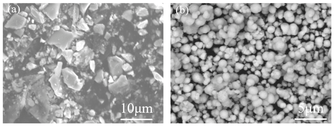
Figure 1. Top-view SEM images of (a) RuO2-1 and (b) RuO2-2.
Materials 19 01734 g001
Figure 2. Top-view SEM images (a,b) and cross-sectional SEM images (c,d) of RuO2-1-coated p-Si (100) 15–25 Ω·cm substrate etched in 0.4 M H2O2-10 M HF solution for 1 h.
Materials 19 01734 g002
Figure 3. Cross-sectional SEM images of etching depth varying with the size of RuO2 particles. The depths of the pores are (a) 7.03 μm; (b) 39.3 μm; (c) 89.7 μm.
Materials 19 01734 g003
Figure 4. EDS elemental mapping images of Si after RuO2-catalyzed etching. (a) Cross-sectional SEM image of the sample. Corresponding elemental mapping of (b) Si; (c) Ru; (d) O.
Materials 19 01734 g004
Figure 5. Cross-sectional SEM images of RuO2-coated Si etched for (a) 10 min; (b) 30 min; (c) 1 h; (d) 2 h.
Materials 19 01734 g005
Figure 6. Top-view SEM images (a,b) and cross-sectional SEM images (c,d) of RuO2-2-coated p-Si (100) 15–25 Ω·cm substrate etched in 0.4 M H2O2-10 M HF solution for 1 h.
Materials 19 01734 g006
Figure 7. XRD pattern of (a) RuO2 and (c) RuO2-coated p-Si (100) 15–25 Ω·cm substrate etched in 0.4 M H2O2-10 M HF solution for 1 h; Deconvoluted XPS spectra of Ru 3d+C 1s of (b) RuO2 and (d) RuO2-coated p-Si (100) 15–25 Ω·cm substrate etched in 0.4 M H2O2-10 M HF solution for 1 h.
Materials 19 01734 g007
Figure 8. (a,b) Top-view SEM images of RuO2-coated p-Si (100) 15–25 Ω·cm substrate etched in the aerated HF/H2O vapor for 5 h; (c,d) Top-view SEM images of RuO2-coated p-Si (100) 15–25 Ω·cm substrate etched in the aerated HF/H2O vapor for 22 h.
Materials 19 01734 g008
Figure 9. (a) Dark cathodic polarization curves of RuO2-plated silicon wafers in HF (pink curve)/HF-H2O2 (purple curve) solution; (b) Dark cathodic polarization curves of silicon wafers in HF-H2O2 solution without RuO2 (red curve) and with RuO2 (blue curve).
Materials 19 01734 g009
Figure 10. Schematic diagrams of (a) MACE mechanism and (b) RuO2-catalyzed silicon etching mechanism.
Materials 19 01734 g010
Table 1. Comparison between MACE and OACE.
MACE (Noble Metals: Ag, Au, Pt, etc.)OACE (This Work: RuO2)
Charge transferOxidant (e.g., H2O2) injects holes into silicon.RuO2 particles inject holes into silicon.
Catalyst behaviorThe valence state of the catalyst remains unchanged; Metal particles move directionally.The valence state of the catalyst changes; RuO2 particles move directionally.
Reaction pathwaysThe oxidant (e.g., H2O2) injects holes into silicon through the catalyst, and the oxidized silicon dissolves in the HF solution.RuO2 is reduced to Ru2O3 after injecting holes into silicon, and the oxidized silicon dissolves in the HF solution. Ru2O3 is reoxidized to RuO2 by H2O2.
Disclaimer/Publisher’s Note: The statements, opinions and data contained in all publications are solely those of the individual author(s) and contributor(s) and not of MDPI and/or the editor(s). MDPI and/or the editor(s) disclaim responsibility for any injury to people or property resulting from any ideas, methods, instructions or products referred to in the content.