3. Results and Discussion
The electrical transport and piezoelectric output characteristics of the h-BN/GaN device were systematically compared with those of the matched released/flexible GaN/Cu reference device fabricated using the same substrate-removal, transfer, and electrode-fabrication processes but without the h-BN layer. Consequently, effects associated with Si-substrate removal, flexible transfer, and process-induced residual-stress relaxation were common to both devices, enabling a more direct evaluation of the effect of h-BN integration.
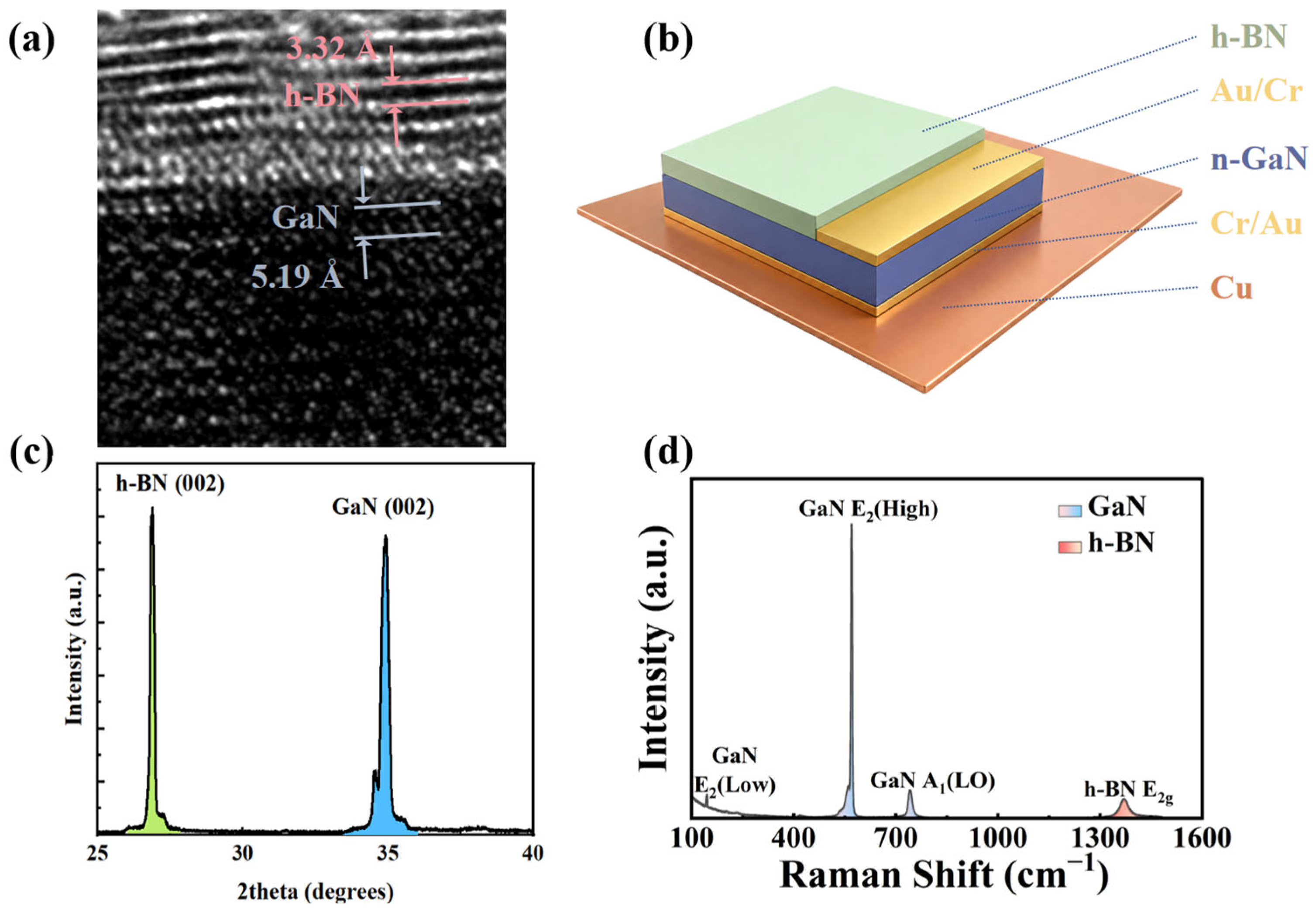
The formation of the h-BN/GaN heterostructure was first examined by cross-sectional high-resolution transmission electron microscopy (HRTEM). As shown in
Figure 2a, a layered h-BN film is clearly observed on the GaN surface, forming a sharp and continuous interface with the underlying GaN. No obvious interfacial voids, cracks, or delamination can be observed, suggesting that the PECVD-grown h-BN is conformally integrated with the GaN layer. Such intimate interfacial contact is particularly important for piezoelectric devices, because efficient stress transfer and interfacial charge coupling strongly depend on the mechanical and electrical continuity across the heterointerface [
34].
The lattice-resolved HRTEM image further reveals ordered lattice fringes in both the h-BN and GaN regions. The interlayer spacing of the upper layered region is measured to be approximately 3.32 Å, which agrees well with the characteristic spacing of the h-BN (002) planes [
35]. This confirms the formation of layered h-BN with its basal planes preferentially aligned parallel to the GaN surface. In the GaN region, a lattice periodicity of approximately 5.19 Å is observed along the c-axis direction, consistent with the wurtzite GaN lattice [
36]. These results indicate that the h-BN layer was successfully grown on GaN while maintaining a well-defined crystalline interface.
Figure 2b illustrates the device architecture constructed from the h-BN/GaN heterostructure. The device consists of a top h-BN layer, a reserved Au/Cr top electrode on the exposed GaN region, an n-type GaN piezoelectric layer, a Cr/Au bottom electrode, and a flexible Cu supporting substrate. In this configuration, GaN serves as the main piezoelectric semiconductor layer, while the h-BN layer provides a thermally robust and electrically insulating interfacial layer. The combination of h-BN and GaN is expected to suppress free-carrier screening at the GaN surface and enhance the stability of strain-induced polarization charges, which provides the structural basis for the subsequent piezoelectric sensing performance.
The crystallographic orientation of the h-BN/GaN heterostructure was further investigated by X-ray diffraction in the 2θ–ω mode, as shown in
Figure 2c. Two dominant diffraction peaks assigned to h-BN (002) and GaN (002) are observed, confirming the coexistence of crystalline h-BN and GaN. The presence of the h-BN (002) reflection indicates that the h-BN film possesses a preferential c-axis orientation, with its basal planes parallel to the GaN surface. Meanwhile, the strong GaN (002) peak confirms the c-axis-oriented wurtzite GaN layer. The simultaneous observation of h-BN (002) and GaN (002) reflections suggests a well-defined out-of-plane orientational relationship between the two materials, consistent with the lattice-resolved HRTEM results.
Raman spectroscopy was employed as a complementary technique to verify the chemical and vibrational signatures of the heterostructure. As shown in
Figure 2d, the spectrum exhibits the characteristic Raman modes of GaN, including the E
2(low), E
2(high), and A
1(LO) modes, indicating that the GaN lattice remains well preserved after PECVD growth of h-BN. In addition, the h-BN E
2g mode is observed at high wavenumber, providing further evidence for the successful formation of h-BN on the GaN surface. The coexistence of GaN and h-BN Raman features, together with the HRTEM and XRD results, confirms the successful construction of a structurally integrated h-BN/GaN heterostructure.
Overall, the combined HRTEM, XRD, and Raman characterizations demonstrate that crystalline h-BN was successfully grown on GaN by PECVD. The resulting heterostructure exhibits a compact interface, clear lattice features, and preferential out-of-plane orientation, which are essential prerequisites for efficient electromechanical coupling and stable operation of the flexible h-BN/GaN piezoelectric device.
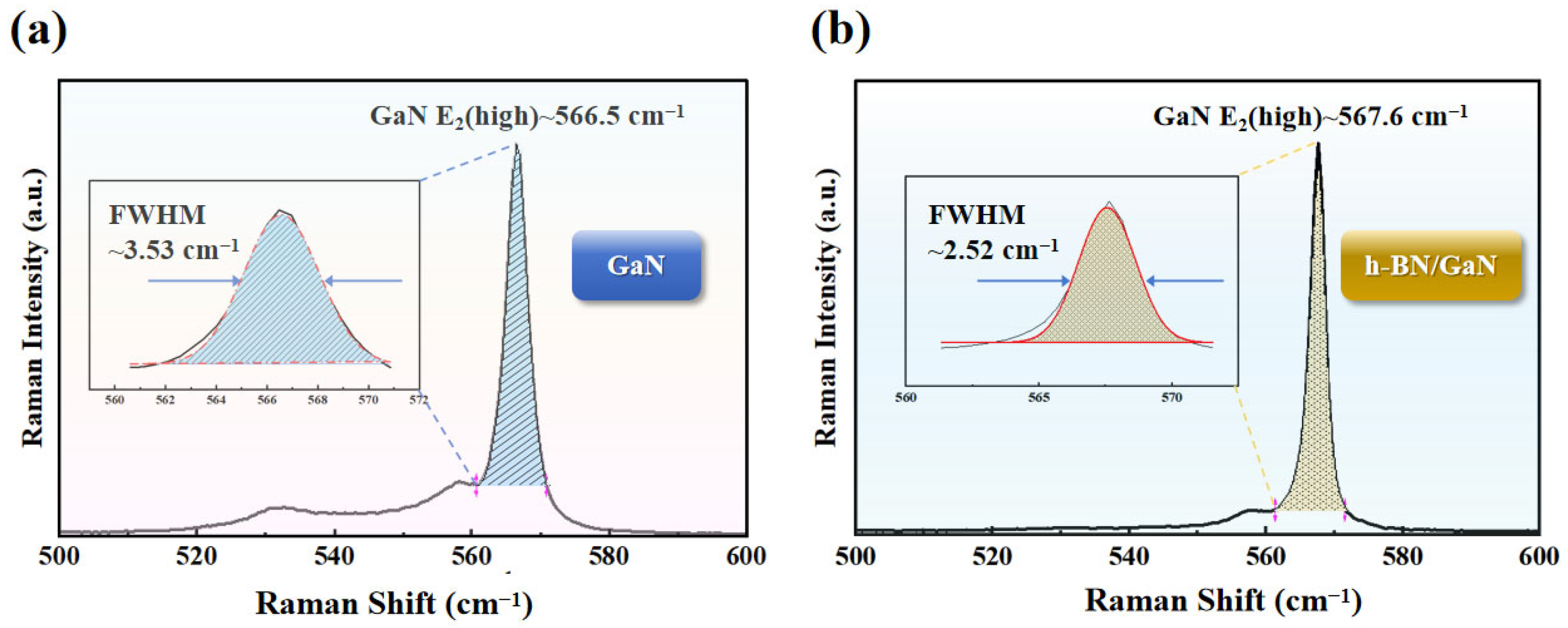
Raman spectroscopy was further employed to evaluate the strain state of GaN before and after device fabrication, as shown in
Figure 3. The nonpolar E
2(high) phonon mode of wurtzite GaN is highly sensitive to residual stress and is therefore commonly used as a fingerprint for strain evaluation. For stress-free GaN, the E
2(high) mode is generally located at approximately 567.5 cm
−1 [
37]. In the as-grown GaN/Si substrate, the E
2(high) peak appears at approximately 566.5 cm
−1, as shown in
Figure 3a. This red shift relative to the stress-free position indicates that the GaN layer grown on Si is subjected to residual tensile stress, which can be attributed to lattice mismatch, thermal expansion mismatch, and the mechanical constraint imposed by the rigid Si substrate.
After the fabrication of the flexible h-BN/GaN/Cu device, the GaN E
2(high) mode shifts to approximately 567.6 cm
−1 as shown in
Figure 3b. The peak position becomes very close to that of stress-free GaN, suggesting that the residual stress in the GaN layer is significantly released during the backside Si removal and flexible transfer process. This stress relaxation is mainly associated with the elimination of the rigid Si substrate constraint. Meanwhile, the conformal h-BN layer and the flexible Cu support may help maintain the structural integrity of the released GaN thin film and suppress local stress concentration during transfer and bending.
In addition to the peak-position shift, the full width at half maximum (FWHM) of the GaN E
2(high) mode decreases from approximately 3.53 cm
−1 for the original GaN substrate to approximately 2.52 cm
−1 for the h-BN/GaN device. The narrower Raman linewidth indicates reduced phonon scattering and suppressed inhomogeneous strain broadening in the released heterostructure. This result suggests that the fabrication process not only preserves the crystalline lattice of GaN but also improves the local strain uniformity of the active piezoelectric layer. Such stress relaxation and structural homogenization are beneficial for piezoelectric sensing, because excessive residual stress and strain fluctuation can disturb the piezoelectric potential distribution and degrade the stability of the output signal [
38].
Therefore, the Raman results demonstrate that the conversion from the rigid GaN/Si substrate to the flexible h-BN/GaN/Cu device effectively releases the residual tensile stress in GaN while maintaining a high-quality lattice response. The h-BN/GaN heterostructure thus provides a mechanically stable platform for subsequent flexible and high-temperature piezoelectric sensing.
The electrical transport and piezoelectric output characteristics of the h-BN/GaN device were systematically evaluated and compared with those of a reference GaN device without the h-BN layer.
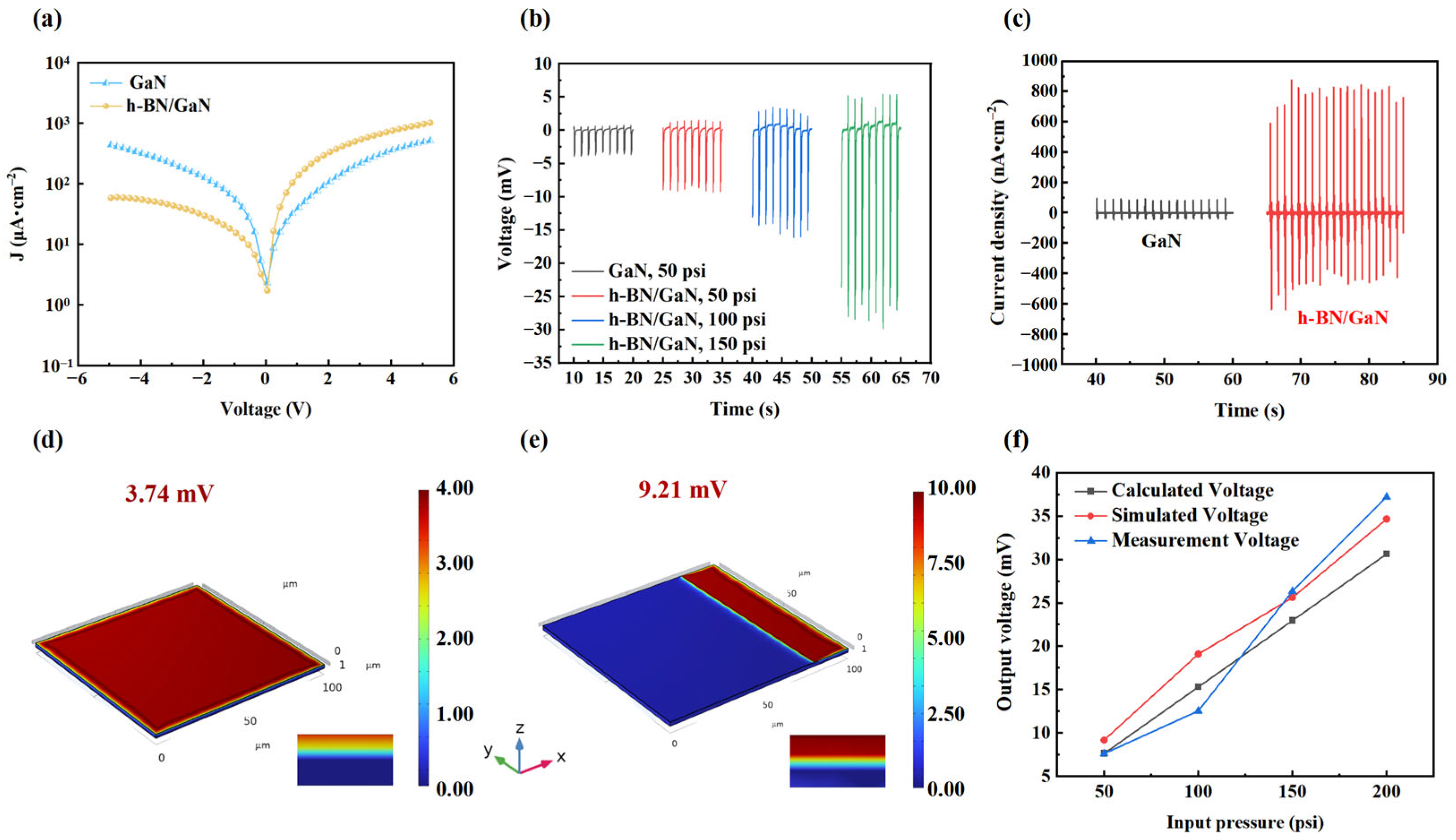
Figure 4a shows the current-density–voltage (J–V) characteristics of the two devices. Compared with the flexible GaN/Cu reference, the h-BN/GaN device exhibits a more asymmetric J–V behavior under positive and negative bias conditions. This non-ohmic transport behavior indicates modified interfacial electrical characteristics after the introduction of h-BN. The wide-bandgap and electrically insulating nature of h-BN can reduce direct carrier transport across the GaN surface and contribute to suppressed leakage under reverse or low-bias conditions. Meanwhile, the enhanced current density under forward bias suggests that the interfacial electronic structure is influenced by the applied electric field, resulting in transport behavior different from simple ohmic conduction.
Such asymmetric transport characteristics suggest the presence of an electrically modulated h-BN/GaN interface, which may influence carrier redistribution and charge compensation processes during piezoelectric operation. However, the J–V asymmetry alone does not uniquely determine the microscopic transport mechanism, as contributions from interface states, contact effects, and other non-ohmic transport processes cannot be fully excluded. Therefore, the role of the h-BN interface in reducing carrier compensation and preserving strain-induced piezoelectric polarization charges is further discussed based on the combined evidence from XPS-derived electronic structure analysis, electrical characterization, and piezoelectric output measurements.
The piezoelectric voltage response was then measured under periodic pressure loading, as shown in
Figure 4b. Under the same pressure of 50 psi, the h-BN/GaN device produces a significantly larger output voltage than the reference GaN device. This enhancement indicates that the incorporation of h-BN effectively improves the electromechanical conversion capability of the GaN-based sensor. For the h-BN/GaN device, the output voltage increases progressively as the applied pressure rises from 50 to 150 psi, demonstrating a clear pressure-dependent response. The stable and repeatable voltage pulses under each pressure condition also indicate good mechanical reliability and reversible piezoelectric response of the flexible heterostructure device.
The output current-density response further confirms the enhanced piezoelectric performance after h-BN integration. As shown in
Figure 4c, the h-BN/GaN device exhibits a much larger transient current-density signal than the GaN reference under dynamic loading. Since piezoelectric current originates from the redistribution of strain-induced polarization charges during loading and unloading, the higher current output suggests that more effective piezoelectric charges are preserved and collected in the h-BN/GaN device. This improvement can be attributed to the combined effects of the interfacial barrier, reduced free-carrier screening in GaN, and enhanced charge separation at the h-BN/GaN interface.
To further understand the influence of h-BN integration on the electromechanical response, finite-element simulations were performed for the GaN and h-BN/GaN structures under identical pressure loading conditions. As shown in
Figure 4d,e, the simulated piezopotential of the h-BN/GaN heterostructure is higher than that of the GaN reference, increasing from approximately 3.74 mV to 9.21 mV.
Within the framework of the present model, this enhancement originates from the modified dielectric boundary condition and electrostatic potential redistribution introduced by the anisotropic h-BN interfacial layer. Compared with GaN (εz = 10.4), h-BN exhibits a lower out-of-plane dielectric constant (εz = 3.76), which modifies the vertical electric-field distribution and potential allocation within the heterostructure. Therefore, the h-BN layer contributes to improved electrostatic potential retention under mechanical excitation.
Although the present electrostatic model does not explicitly describe dynamic carrier transport, interface-state evolution, or time-dependent charge redistribution, the simulated potential variation provides complementary insight into the role of the h-BN interface. Combined with the XPS, electrical, and transient measurements, these results support the proposed interfacial modulation mechanism responsible for the enhanced piezoelectric response.
Figure 4f compares the analytical calculation, finite-element simulation, and experimental output voltages under different pressure conditions. All three results exhibit an approximately linear increase with increasing pressure, indicating that the analytical model and finite-element simulation capture the first-order pressure-dependent electromechanical behavior of the device.
The slight deviations between the calculated, simulated, and experimental values originate from the idealized uniform-pressure assumption, practical stress-transfer conditions, electrode effects, and interfacial nonidealities. Nevertheless, the consistent pressure-dependent trend demonstrates that the h-BN/GaN heterostructure maintains an enhanced piezoelectric response compared with the GaN reference.
According to the simplified parallel-plate capacitor model reported in previous studies, the output voltage of a piezoelectric film under uniform pressure can be expressed as [
13]:
where
Vout is the output voltage, σ is the pressure-induced surface charge density, A is the effective electrode area,
C is the capacitance of the piezoelectric film, e is the piezoelectric coefficient,
P is the applied pressure,
E is the Young’s modulus,
k is the relative dielectric constant,
ε0 is the vacuum permittivity, and
t is the film thickness. In this model, the pressure-induced strain is approximated as
P/
E, and the capacitance is given by
C = kε0A/
t.
For the present h-BN/GaN heterostructure device, GaN is regarded as the dominant piezoelectric layer. Since the top electrode is directly deposited on the GaN surface, the h-BN layer is not treated as an additional dielectric layer connected in series with GaN. To retain the compact scalar form of Equation (1) while accounting for the anisotropic out-of-plane electromechanical response of c-axis-oriented wurtzite GaN, an effective anisotropy correction factor, η
eff, is introduced:
where
eeff,
tGaN,
εr,GaN, and
EGaN represent the effective piezoelectric coefficient, GaN thickness, scalar relative dielectric constant, and scalar Young’s modulus used in the simplified analytical model, respectively. The correction factor
ηeff was independently estimated from the anisotropic elastic and dielectric properties of wurtzite GaN according to
where
Ec and
ε33 are the effective Young’s modulus and relative permittivity along the c-axis, respectively. For hexagonal wurtzite GaN, the effective c-axis Young’s modulus can be expressed as
Using the experimentally reported elastic constants of wurtzite GaN,
C11 = 390 GPa,
C12 = 145 GPa,
C13 = 106 GPa, and
C33 = 398 GPa [
39], the effective c-axis Young’s modulus is calculated to be
Ec ≈ 356 GPa. The out-of-plane relative permittivity of GaN was taken as
ε33 = 10.4, consistent with reported anisotropic dielectric data for wurtzite GaN [
40]. Relative to the scalar reference values
EGaN = 2.5 × 10
11 Pa, and ε
r,GaN = 8.9 used in the simplified analytical model, the resulting anisotropy correction factor is
Therefore, ηeff = 0.60 was adopted in the analytical calculation. This value was determined from the independently reported anisotropic elastic and dielectric parameters of GaN.
In the calculation, the following parameters were used:
eeff = 0.73 C m
−2,
tGaN = 1.0 μm,
ε0 = 8.854 × 10
−12 F·m
−1,
εr,GaN = 8.9, and
EGaN = 2.5 × 10
11 Pa [
41]. Considering the non-ideal characteristics of the practical device, η
eff was taken as 0.60. Under applied pressures of 50, 100, 150, and 200 psi, the calculated output voltages were 7.66, 15.33, 22.99, and 30.66 mV, respectively. The analytical model is used as a first-order description of the pressure-dependent piezoelectric output and is not intended to explicitly describe free-carrier screening or interfacial carrier dynamics.
Taken together, the electrical characterization, dynamic piezoelectric measurements, and simulation results demonstrate that the introduction of h-BN significantly enhances the output performance of GaN-based piezoelectric sensors. The h-BN layer not only forms a barrier-type interface that suppresses free-carrier screening in n-GaN, but also improves interfacial charge separation and piezopotential preservation. These effects collectively contribute to the higher voltage output, larger current-density response, and good pressure-dependent linearity of the flexible h-BN/GaN/Cu piezoelectric device.
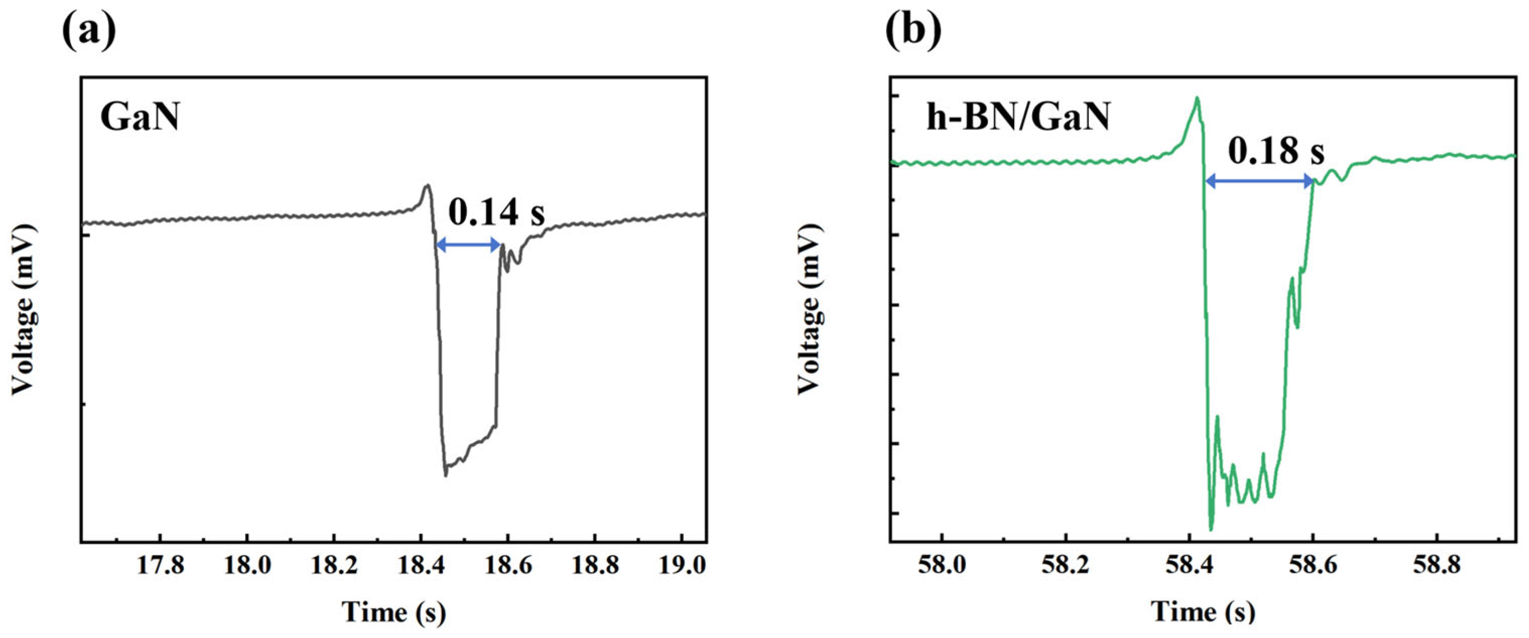
To further compare the transient voltage characteristics of the GaN and h-BN/GaN devices, enlarged views of individual output-voltage pulses were analyzed, as shown in
Figure 5. For the reference GaN device, the voltage signal rapidly decays after mechanical stimulation, with a characteristic pulse duration of approximately 0.14 s (
Figure 5a). The relatively short voltage-retention time indicates a rapid decay of the strain-induced piezoelectric potential after the removal of external loading, which is consistent with efficient charge compensation processes in n-type GaN.
In contrast, the h-BN/GaN device exhibits a longer transient voltage duration of approximately 0.18 s under the same testing conditions (
Figure 5b). The extended voltage-retention behavior suggests that the piezoelectric potential generated in GaN can be maintained for a longer period after h-BN integration. This enhanced charge-retention behavior is attributed to the modified interfacial electrical environment introduced by the h-BN layer, which may influence carrier redistribution and charge compensation processes at the heterointerface. In addition, the insulating h-BN layer may modify the effective capacitance and equivalent RC relaxation behavior of the device, which could also contribute to the prolonged transient voltage decay.
The prolonged voltage pulse observed in the h-BN/GaN device provides complementary evidence that h-BN integration improves piezopotential preservation and transient signal retention. Together with the enhanced output voltage, current density, and XPS-derived interfacial electronic structure modulation, these results suggest that the h-BN/GaN heterostructure provides a more favorable interfacial environment for maintaining piezoelectric charge generation and signal stability compared with the single GaN device.
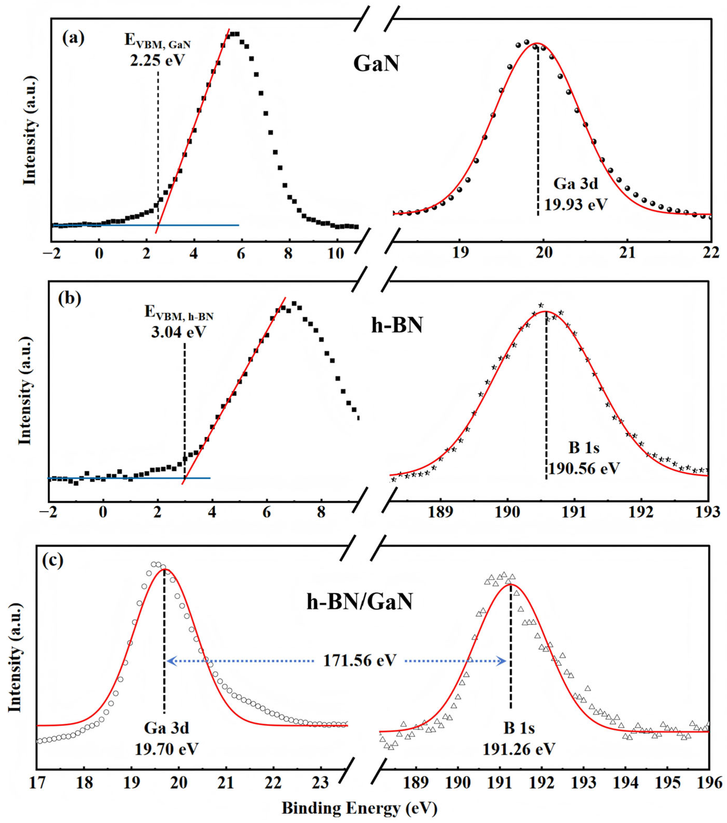
To directly investigate the electronic structure of the h-BN/GaN interface, XPS valence-band and core-level measurements were further performed. As shown in
Figure 6a, the valence-band maximum (
) and Ga 3d core level (
) of the GaN reference are located at 2.25 and 19.93 eV, respectively, corresponding to
eV. For h-BN, the VBM (
) and B 1s core level (
) are located at 3.04 and 190.56 eV, respectively, giving
eV (
Figure 6b). At the h-BN/GaN interface, the Ga 3d (
) and B 1s (
) core levels are observed at 19.70 and 191.26 eV, respectively, resulting in an interfacial core-level separation (
) of 171.56 eV (
Figure 6c). According to the Kraut method [
42],
the valence-band offset
is therefore calculated to be approximately 1.72 eV. Taking the band gaps of GaN and h-BN as 3.40 and 5.90 eV [
43,
44], respectively, the corresponding conduction-band offset
is approximately 0.78 eV. The resulting band alignment therefore reveals a substantial electron-blocking conduction-band discontinuity at the h-BN/GaN heterointerface.
Notably, the Ga 3d core level shifts from 19.93 eV for the GaN reference to 19.70 eV after formation of the h-BN/GaN interface. The approximately 0.23 eV shift toward lower binding energy is consistent with upward band bending on the n-GaN side of the interface, suggesting depletion-like redistribution of mobile electrons near the heterointerface. The experimentally determined band offset and interfacial band bending thus provide an electronic-structure basis for reducing the availability of free electrons that can compensate strain-induced piezoelectric polarization charges. Accordingly, the enhanced piezoelectric response is attributed to an interfacial-barrier-assisted preservation of the GaN piezopotential. It should be noted that static XPS probes the equilibrium electronic structure rather than the dynamic carrier-screening process itself; therefore, suppression of free-carrier screening is supported by the combined XPS, electrical, transient-response, and piezoelectric measurements.
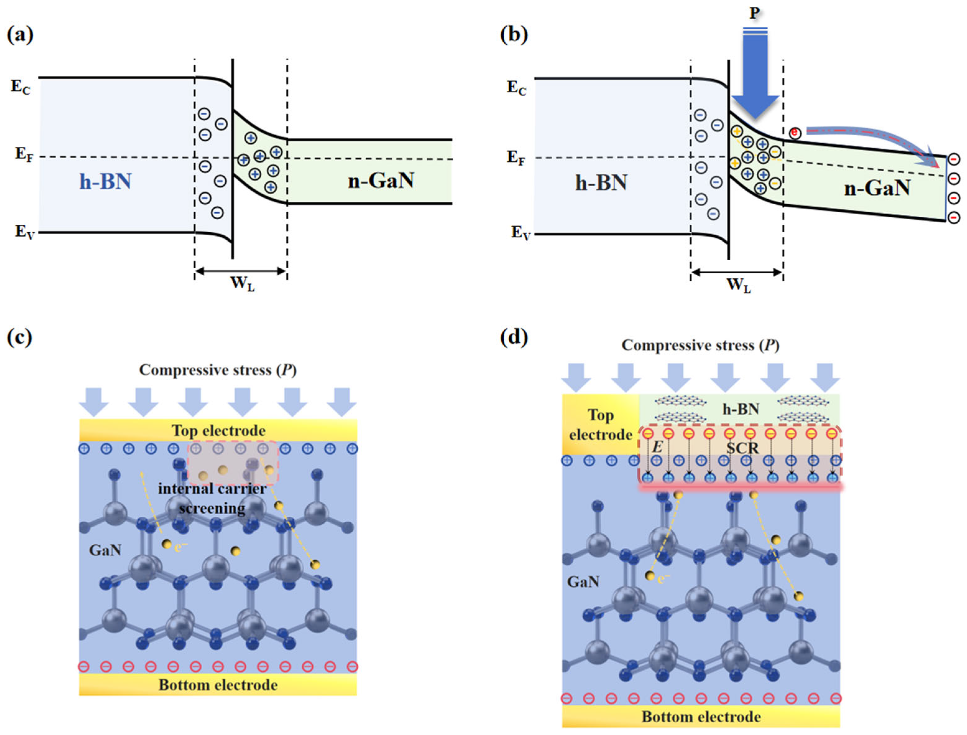
Based on the structural, electrical, and piezoelectric characterizations discussed above, the enhancement mechanism of the h-BN/GaN piezoelectric device is schematically illustrated in
Figure 7. The key role of h-BN is not only to serve as a thermally stable and electrically insulating surface layer, but also to construct a barrier-type heterointerface with n-GaN, thereby regulating the redistribution of free carriers under mechanical deformation.
Figure 7a shows the equilibrium energy-band diagram of the h-BN/n-GaN heterostructure before external pressure is applied. Since the unintentionally doped GaN layer exhibits weak n-type conductivity, with a measured electron concentration of approximately 5 × 10
16 cm
−3, mobile electrons are present in the GaN layer and can participate in charge compensation. After contact with h-BN, interfacial charge redistribution occurs until the Fermi levels tend to align, leading to band bending on the GaN side and the formation of a depletion-like space charge region near the h-BN/GaN interface. In this region, the concentration of mobile electrons is reduced, and an internal electric field is established. This interfacial barrier is consistent with the asymmetric J–V behavior observed in
Figure 4a, indicating that carrier transport across the h-BN/GaN interface is no longer purely ohmic but is modulated by the interfacial potential barrier.
When compressive stress is applied, the non-centrosymmetric wurtzite GaN layer generates piezoelectric polarization charges, as illustrated in
Figure 7b. In bare n-GaN, these piezoelectric charges can be rapidly compensated by free electrons, resulting in strong carrier screening and a reduced effective piezopotential. In contrast, in the h-BN/GaN heterostructure, the pre-existing depletion-like region near the interface acts as a carrier-depleted protection layer, which suppresses the rapid migration of free electrons toward the piezoelectric polarization charges. As a result, a larger fraction of the strain-induced piezopotential can be preserved. Meanwhile, the generated piezopotential transiently perturbs the original band equilibrium and modulates the interfacial band bending. This strain-induced modulation can drive electron redistribution away from the interfacial region and toward the opposite side of the GaN layer, further strengthening the effective potential difference between the two electrodes.
The difference between the bare GaN and h-BN/GaN devices can be further understood from the carrier-screening models shown in
Figure 7c,d. For the GaN reference (
Figure 7c), compressive stress induces polarization charges at the GaN surfaces. However, because the GaN layer contains residual free electrons, these electrons can rapidly migrate and neutralize the positive piezoelectric charges near the stressed surface. This internal carrier screening weakens the piezoelectric potential, leading to the relatively low voltage and current-density outputs observed for the reference GaN device in
Figure 4b,c. It also explains the shorter transient voltage duration shown in
Figure 5a, where the generated voltage decays rapidly after mechanical stimulation.
After h-BN integration, the h-BN/GaN interface forms a space charge region that separates the mobile carriers in GaN from the strain-induced polarization charges, as shown in
Figure 7d. The insulating h-BN layer and the interfacial barrier jointly hinder fast electron compensation, allowing the piezoelectric potential to be maintained for a longer time. This mechanism is supported by the enhanced voltage and current-density outputs of the h-BN/GaN device in
Figure 4b,c, the larger simulated piezopotential of the h-BN/GaN structure in
Figure 4d,e, and the prolonged transient voltage duration in
Figure 5b. Therefore, the improved piezoelectric response of the h-BN/GaN device originates from the combined effects of interfacial depletion, suppressed free-carrier screening, and strain-induced barrier modulation.
Overall, the h-BN/GaN heterostructure provides an effective piezotronic interface for preserving and amplifying the piezoelectric potential generated in GaN. The interfacial space charge region reduces rapid electron screening, while the pressure-induced piezopotential dynamically modulates the band bending and charge distribution across the heterointerface. This mechanism accounts for the higher output voltage, larger current-density response, improved voltage retention, and good pressure-dependent behavior of the flexible h-BN/GaN/Cu piezoelectric sensor.
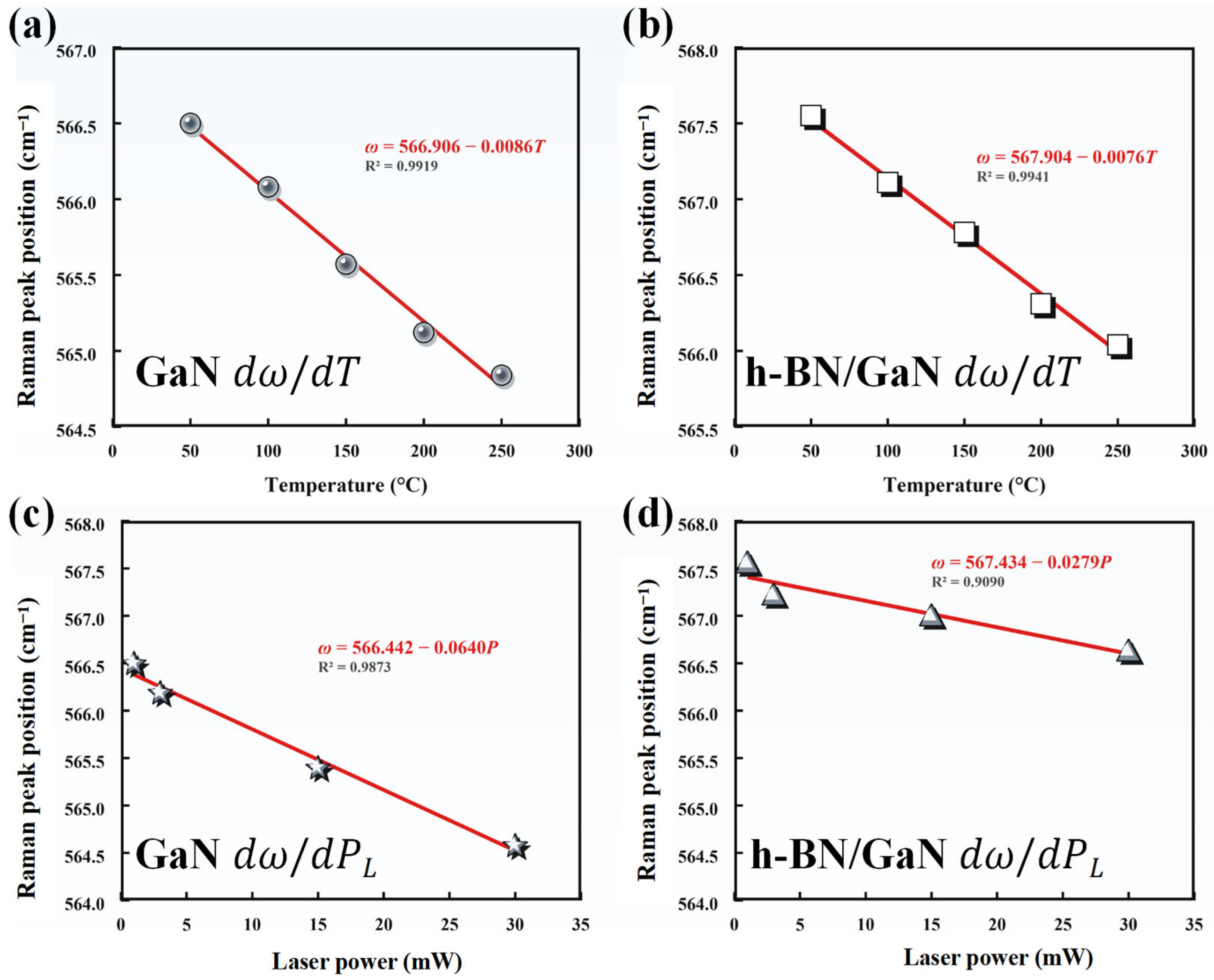
In addition to electromechanical conversion, thermal management is another critical requirement for piezoelectric sensors operating in harsh environments. Since the device consists of micron-scale thin films, conventional bulk thermal-conductivity measurement methods are difficult to apply directly. Raman optothermal analysis was therefore employed to evaluate the local heat-dissipation behavior of the GaN and h-BN/GaN devices by monitoring the temperature- and laser-power-dependent shift in the GaN E2(high) phonon mode.
Figure 8a,b show the temperature-dependent Raman peak positions of the GaN E2(high) mode for the bare GaN and h-BN/GaN devices, respectively. In both cases, the Raman peak exhibits a nearly linear red shift with increasing temperature, which is mainly attributed to lattice thermal expansion and anharmonic phonon–phonon interactions. The fitted temperature coefficients are (−0.0086) cm
−1/°C for GaN and (−0.0076) cm
−1/°C for h-BN/GaN, indicating comparable thermally induced phonon softening in the two structures. These temperature coefficients provide the necessary calibration for converting laser-induced Raman shifts into local temperature variations.
The laser-power-dependent Raman measurements are shown in
Figure 8c,d. As the laser power increases, local optical heating causes a red shift in the GaN E
2(high) mode. For the GaN reference, the fitted power coefficient is (−0.0640) cm
−1/mW, whereas the h-BN/GaN device shows a much smaller value of (−0.0279) cm
−1/mW. The significantly reduced magnitude of
dω/
dPL indicates that, under the same laser excitation, the GaN layer in the h-BN/GaN device experiences a smaller local temperature rise. This result suggests that the introduction of h-BN facilitates more efficient heat spreading and suppresses localized self-heating in the active piezoelectric region.
According to Raman optothermal analysis, the effective thermal transport capability can be qualitatively compared using the relationship (K ∝ (
dω/
dT)/
(dω/
dPL)) [
45]. The relative thermal response extracted from the Raman optothermal measurements indicates that the h-BN/GaN heterostructure exhibits a lower local temperature rise compared with the GaN reference under identical optical excitation conditions. This improvement is attributed to the high thermal stability and heat-spreading capability of h-BN, together with its intimate interfacial contact with GaN, as confirmed by the structural characterization in
Figure 2. The improved thermal dissipation can reduce heat accumulation in the GaN piezoelectric layer, thereby helping to maintain stable polarization and output signals under elevated-temperature operation.
These Raman optothermal results provide additional evidence that h-BN integration not only enhances the piezoelectric output through interfacial charge regulation, as discussed in
Figure 4,
Figure 5,
Figure 6 and
Figure 7, but also improves the thermal-management characteristics of the device. Such combined electromechanical and thermal advantages are essential for reliable operation of the h-BN/GaN piezoelectric sensor in harsh environments.
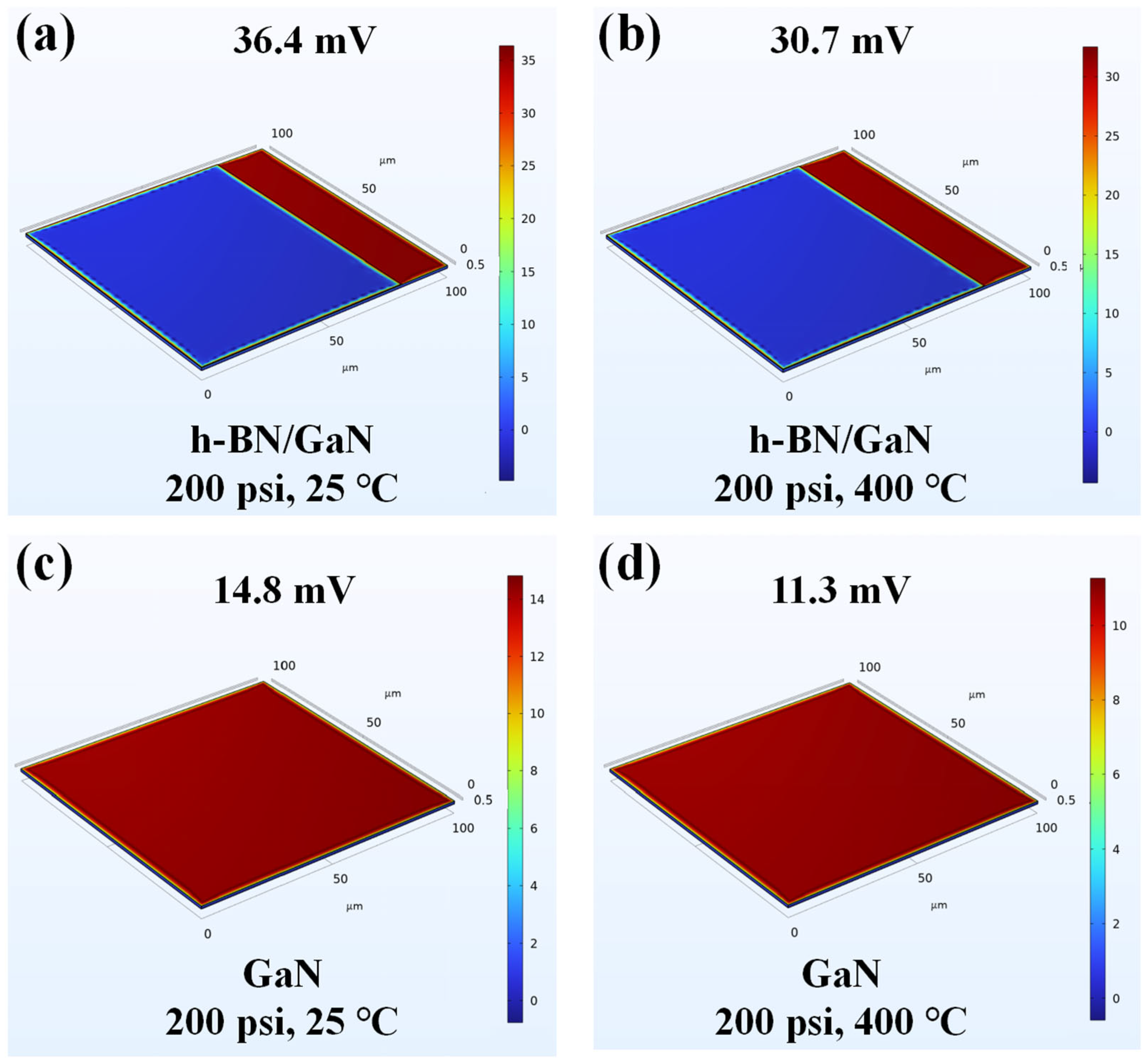
To evaluate the temperature dependence of the electrostatic response, finite-element calculations were performed under an identical nominal pressure of 200 psi while the temperature-dependent dielectric and electromechanical parameters were varied from 298.15 to 673.15 K. At room temperature, the h-BN/GaN structure exhibits a maximum modeled potential of approximately 36.4 mV, compared with 14.8 mV for the GaN reference (shown in
Figure 9).
The higher simulated potential indicates that the introduction of h-BN modifies the electrostatic response of the heterostructure and promotes more effective potential retention under mechanical excitation. This behavior is consistent with the experimentally observed enhancement of the h-BN/GaN piezoelectric output.
At 400 °C, the modeled potentials decrease to approximately 30.7 mV for h-BN/GaN and 11.3 mV for GaN. The corresponding voltage attenuation from room temperature to 400 °C is approximately 15.7% and 23.6%, respectively. These results indicate that the h-BN/GaN structure exhibits improved thermal retention of the electrostatic/piezopotential response compared with the GaN reference.
The reduced temperature-induced degradation suggests that the h-BN interfacial layer contributes to maintaining the electromechanical response of the heterostructure under harsh thermal conditions. This trend agrees well with the experimental observation that the h-BN/GaN device preserves higher output performance at elevated temperatures.
Therefore, the simulation results provide further support for the enhancement mechanism proposed in
Figure 7. The h-BN/GaN heterostructure not only increases the piezopotential output under the same pressure loading, but also mitigates thermal degradation of the voltage response. These advantages are critical for piezoelectric sensing applications in harsh environments where both mechanical pressure and elevated temperature are present.
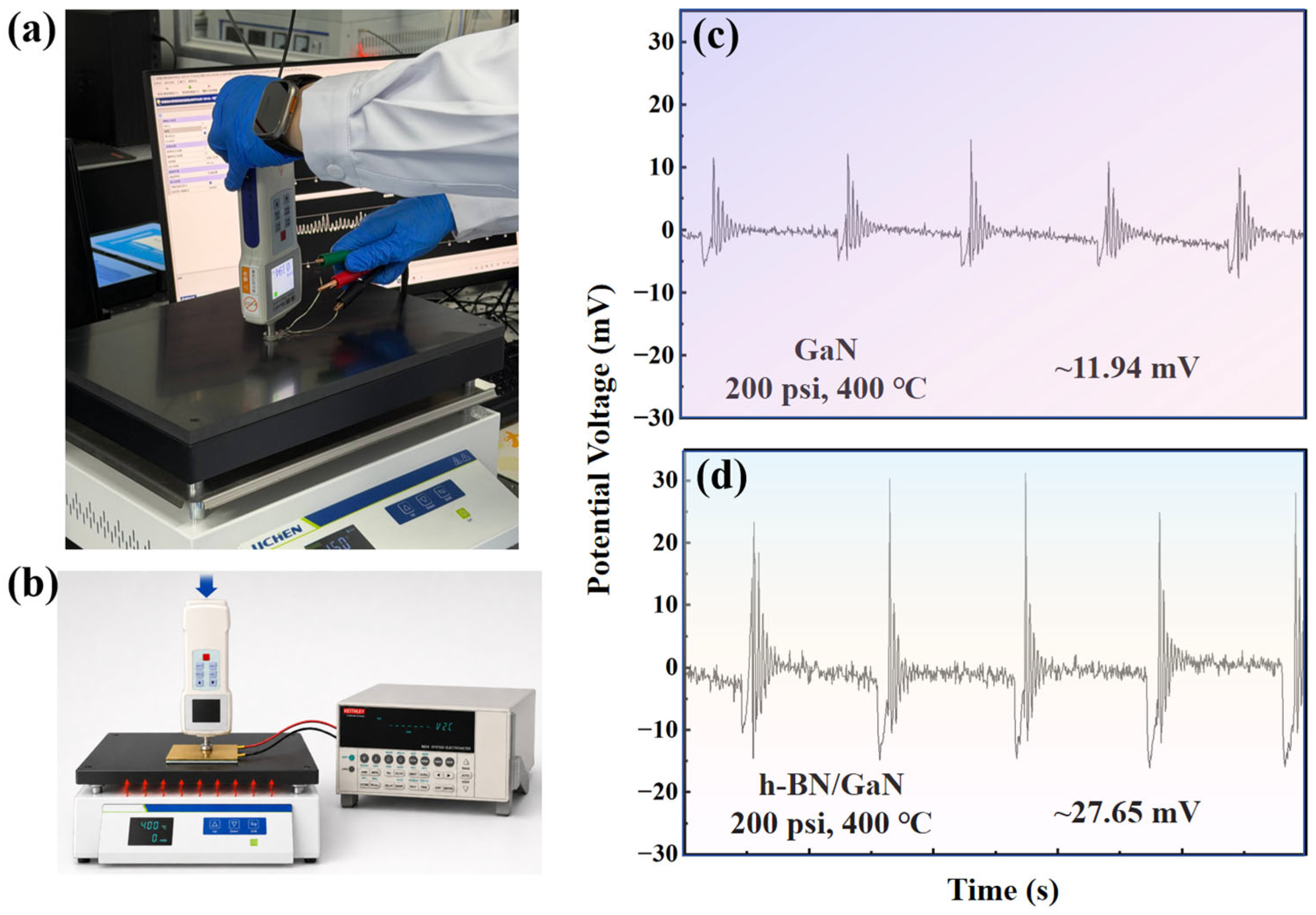
To further verify the practical applicability of the h-BN/GaN piezoelectric device under harsh environments, high-temperature pressure-response measurements were performed at 400 °C, as shown in
Figure 10.
Figure 10a presents the photograph of the experimental setup, in which a force gauge was used to apply periodic pressure to the flexible device placed on a heating stage. A schematic illustration of the measurement configuration is shown in
Figure 10b. During testing, the device was subjected to repeated compressive loading while the output voltage was recorded by an electrometer. This configuration enables direct evaluation of the piezoelectric response under coupled high-temperature and mechanical-pressure conditions.
Figure 10c,d compare the output voltage signals of the bare GaN and h-BN/GaN devices under 200 psi at 400 ℃. The GaN reference exhibits a relatively weak voltage response, with an output amplitude of approximately 11.94 mV. In contrast, the h-BN/GaN device maintains a much higher output voltage of approximately 27.65 mV under the same testing condition. The output voltage of the h-BN/GaN device is therefore about 2.32 times that of the GaN reference at 400 °C, demonstrating that the h-BN/GaN heterostructure remains effective in enhancing piezoelectric output even under elevated-temperature operation.
The experimental high-temperature results are also consistent with the temperature-dependent finite-element simulation shown in
Figure 9, where the simulated output voltages at 400 ℃ were 11.3 mV for bare GaN and 30.7 mV for h-BN/GaN. Although slight differences between simulation and experiment are expected because of nonideal contact, actual pressure distribution, thermal gradients, electrode resistance, and packaging effects, the overall trend and voltage magnitude agree well. This agreement further supports the proposed mechanism that h-BN integration can help preserve the piezopotential in GaN by suppressing free-carrier screening and stabilizing the interfacial electric field.
More importantly, the h-BN/GaN device exhibits repeatable voltage pulses at 400 ℃, indicating that the all-inorganic heterostructure maintains stable electromechanical conversion under harsh thermal–mechanical conditions. The stable voltage pulses obtained under repeated loading demonstrate good cycle-to-cycle repeatability and reversible piezoelectric response of the representative h-BN/GaN device. It should be emphasized that these repeated measurements characterize the repeatability of an individual device and are not intended to establish device-to-device statistical reproducibility. Combined with the Raman optothermal analysis in
Figure 8, which suggests improved heat-dissipation capability after h-BN integration, these high-temperature pressure-response results confirm that the h-BN/GaN/Cu device possesses strong potential for pressure sensing in high-temperature industrial environments.
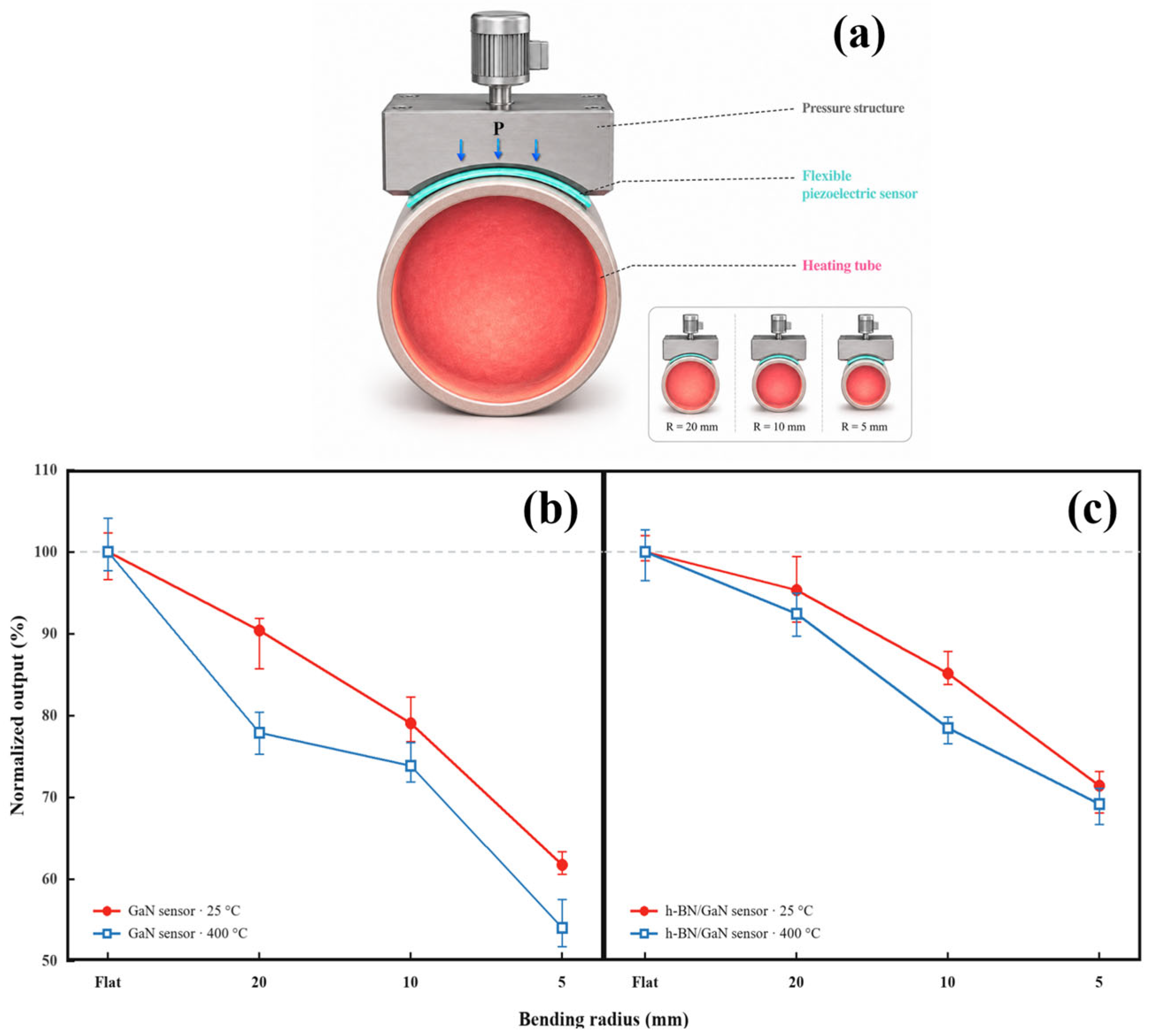
To further evaluate the mechanical flexibility and thermal operational stability of the flexible piezoelectric sensors, a curvature-controlled high-temperature bending platform was developed, as illustrated in
Figure 11a. Different bending radii were achieved by replacing cylindrical heating tubes with different diameters, while a matching pressure head fabricated by mechanical machining was used to ensure conformal contact between the loading structure and the flexible sensor. The flexible h-BN/GaN and GaN reference devices were subjected to repeated bending deformation and continuous piezoelectric operation under controlled temperature conditions.
For each bending radius and temperature condition, five independently fabricated devices were tested. The normalized output was calculated based on the average peak voltage after 1000 bending cycles and 1 h continuous pressure loading. The error bars represent the maximum and minimum values among the five tested devices, reflecting the device-to-device variation.
As shown in
Figure 11b, the GaN reference devices exhibit a gradual decrease in normalized output with decreasing bending radius. At room temperature, the normalized output decreases from 100% under flat conditions to approximately 90%, 79%, and 62% at bending radii of 20, 10, and 5 mm, respectively. After high-temperature operation at 400 °C, the output retention further decreases, reaching approximately 78%, 74%, and 54% at the corresponding bending radii. In comparison, the h-BN/GaN heterostructure demonstrates improved mechanical and thermal stability. At room temperature, the output retention remains approximately 95%, 85%, and 71% at bending radii of 20, 10, and 5 mm, respectively. More importantly, after continuous operation at 400 °C, the h-BN/GaN device maintains higher output retention of approximately 92%, 78%, and 69% under the same bending conditions.
The improved retention under bending and elevated temperature is attributed to the enhanced interfacial stability and mechanical compliance provided by the h-BN/GaN heterostructure. The atomically thin h-BN interfacial layer can accommodate local strain redistribution while maintaining stable electronic coupling at the heterointerface, which contributes to improved robustness during combined mechanical and thermal stresses. These results demonstrate that the h-BN/GaN flexible piezoelectric sensor maintains stable electromechanical performance under repeated bending deformation and elevated-temperature operation, providing further evidence of its suitability for harsh-environment sensing applications.
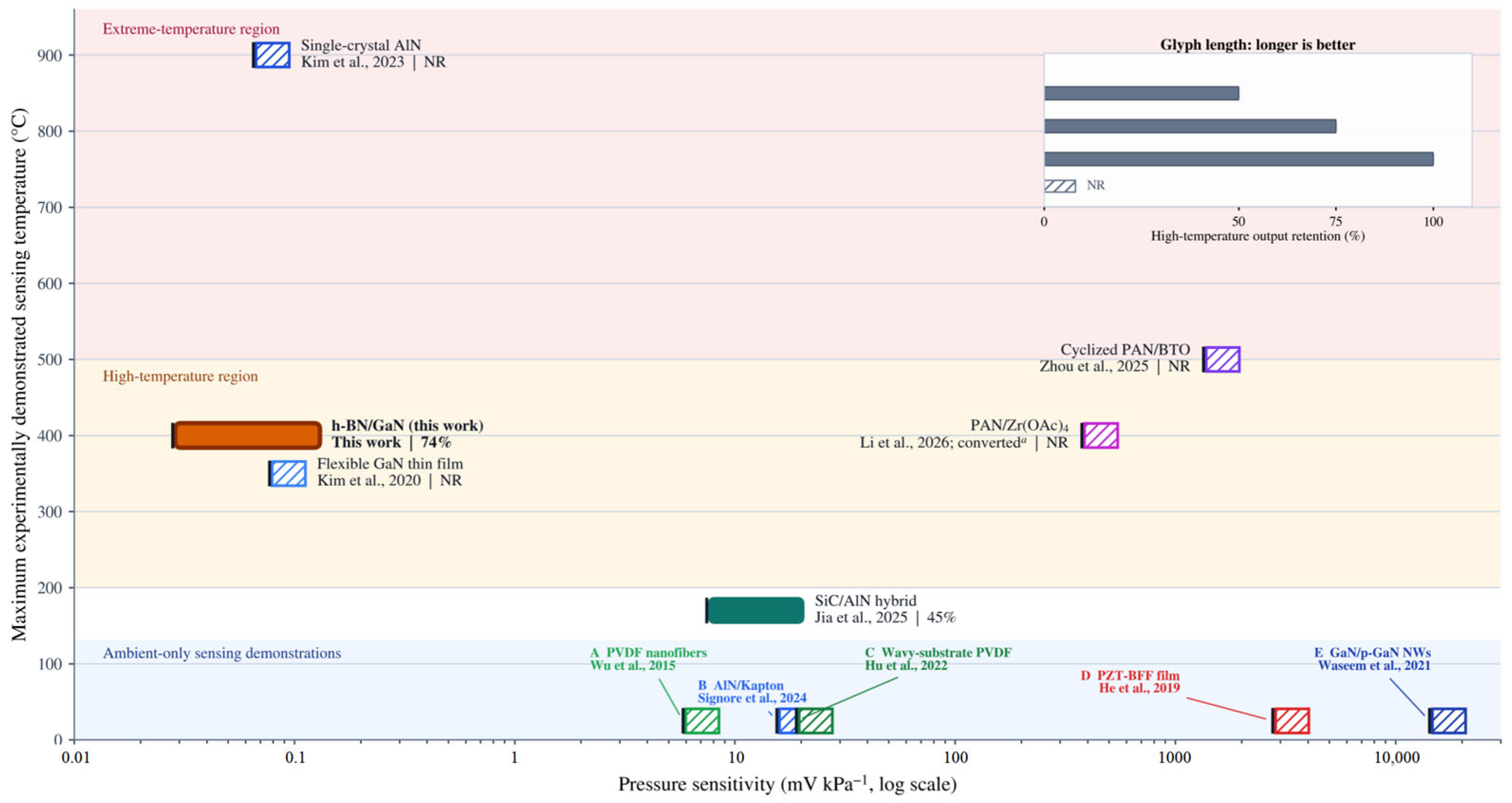
To further clarify the advantages of the proposed h-BN/GaN heterostructure, a quantitative comparison with previously reported piezoelectric sensors was performed, as summarized in
Figure 12. The comparison includes representative flexible and harsh-environment piezoelectric devices based on polymer, ceramic, and wide-bandgap semiconductor materials, considering key parameters including experimentally demonstrated operating temperature, pressure sensitivity, output retention, device architecture, and mechanical flexibility.
Conventional flexible piezoelectric materials such as PVDF-based devices generally exhibit excellent mechanical compliance and high pressure sensitivity; however, their practical application in high-temperature environments is limited by the thermal instability of polymer matrices. Conversely, ceramic piezoelectric materials and wide-bandgap semiconductor piezoelectric sensors, including PZT-, AlN-, SiC-, and GaN-based devices, provide improved thermal tolerance but are commonly fabricated on rigid substrates or bulk structures, limiting their mechanical adaptability.
Recent advances in flexible GaN-based piezoelectric sensors have demonstrated the feasibility of combining semiconductor piezoelectricity with flexible substrates. However, maintaining stable piezoelectric output under elevated temperatures remains challenging because of carrier compensation, interfacial charge loss, and thermomechanical instability. As shown in
Figure 12, the present h-BN/GaN heterostructure simultaneously achieves high-temperature operation at 400 °C and flexible thin-film integration, while maintaining approximately 74% output retention after high-temperature operation. This combination distinguishes the present device from previously reported flexible piezoelectric sensors, which typically exhibit either high sensitivity at ambient conditions or high-temperature capability without mechanical flexibility.
The enhanced performance originates from the synergistic role of the h-BN/GaN heterointerface. Unlike conventional GaN devices that mainly rely on the intrinsic piezoelectric response of GaN, the introduction of h-BN provides an electrically and mechanically stable interfacial layer, which modifies the local charge environment, improves piezopotential preservation, and enhances structural robustness under combined thermal and mechanical stresses. Therefore, the key advancement of this work is not only the extension of the operating temperature of flexible GaN-based piezoelectric sensors, but also the realization of an integrated strategy combining high-temperature stability, mechanical flexibility, and reliable piezoelectric output.



 ,
,