

Review

An Overview of Chromic Transition Metal Oxide Thin Films

by
Gheorghe Ghilețchii
1,
Alexandru Varzari
1,
Ştefan-Andrei Irimiciuc
2,3,*,
Ján Lančok
2 and
Sergiu Vatavu
1
1
Physics of Semiconductors and Devices Lab, Faculty of Physics and Engineering, Moldova State University, 2009 Chisinau, Moldova
2
Institute of Physics of the Czech Academy of Science, 182 00 Prague, Czech Republic
3
National Institute for Laser, Plasma and Radiation Physics, 077125 Magurele, Romania
*
Author to whom correspondence should be addressed.
Materials 2026, 19(14), 2943; https://doi.org/10.3390/ma19142943
Submission received: 18 May 2026 / Revised: 25 June 2026 / Accepted: 1 July 2026 / Published: 8 July 2026

Abstract

Transition metal oxides constitute an important materials platform for chromic phenomena because their optical response is strongly coupled to the changes in electronic structure, phase state, carrier concentration, and defect chemistry. This review discusses selected transition metal oxide thin films, with emphasis on VO2 and other vanadium oxides, WO3, NiO, and TiO2. The review summarizes the structural and electronic characteristics of these representative oxide systems and highlights the role of phase composition, crystal structure, oxygen non-stoichiometry, and defect chemistry in determining their optical response. The main thin film preparation routes, including pulsed laser deposition, magnetron sputtering, sol–gel and aerosol spray methods, atomic layer deposition, chemical vapor deposition, electrochemical routes, and molecular beam epitaxy, are reviewed with respect their influence on obtained thin films. Particular attention is given to applications in thermochromic VO2-and electrochromic WO3/NiO-based smart windows, and transition metal oxide-based gasochromic hydrogen sensors. Key challenges related to transition temperature tuning, luminous transmittance, solar modulation, optical contrast, cycling stability, ion transport and large-area integration are also discussed. Overall this review provides a comparative overview of selected transition metal oxide thin films by connecting material chemistry and physics, thin film preparation technology and functionality.

1. Introduction

Smart materials are materials capable of undergoing reversible and controllable changes in their physical or chemical properties under external stimuli such as temperature, light, electric field, mechanical stress, gas atmosphere, or chemical environment [1,2,3]. Unlike conventional materials, which are usually regarded as passive static systems with fixed functional parameters, smart materials behave as dynamic systems whose response can adapt to changing operating conditions. Their ability to modulate electrical, optical, magnetic, mechanical, or thermal properties makes them relevant to the transition from static material platforms toward responsive and adaptive systems.
Within this broader group, materials with adaptive optical response form a particularly important subgroup, since external stimuli can directly modify optical transmittance, reflectance, absorption, apparent color, or thermal emissivity. Such control over light–matter interaction is especially valuable because optical response is immediately linked to visual perception, daylight and solar energy management, thermal regulation, and signal readout. From a technological point of view, these changes can be readily monitored visually or spectroscopically, which facilitates their use in coatings, smart windows (SWs), sensors, and other optoelectronic devices [4,5,6,7,8]. Among these materials, chromic systems are of particular interest because they reversibly modulate the spectral response and/or visible appearance under external stimuli.
Chromic materials are actively investigated for smart and energy-efficient windows, building-integrated thermal-management coatings, optical and gas-sensing systems, visual indicators, adaptive camouflage, information-storage and display-related concepts, and thin film optoelectronic devices [5,8,9,10,11].
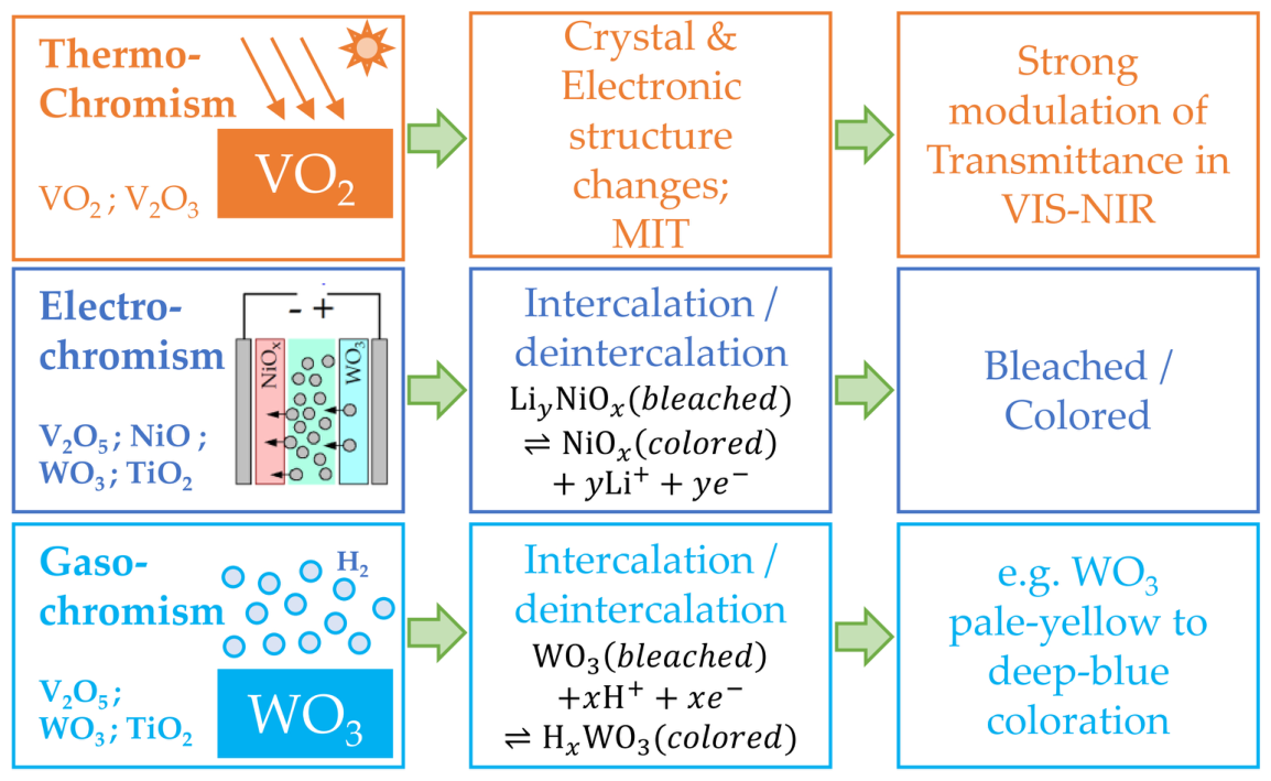
Transition metal oxides (TMOs) constitute a broad class of inorganic materials with a remarkable diversity of crystal structures and of structural, electronic, and optical properties [12]. Depending on composition, bonding geometry, and correlation strength, TMOs can behave as both band insulators (or semiconductors) and correlated metal. In addition, many TMOs exhibit metal-insulator (MIT) phase transitions, magnetism, multiferroicity, and other emergent phenomena [13]. Owing to this versatility, TMOs have become an important functional platform for electronics, optoelectronics, sensing, and energy-related technologies [14,15,16]. For chromic functionality, TMOs are especially attractive because their optical response is strongly coupled to their electronic and structural state [13]. Changes in carrier concentration, oxidation state, defect chemistry, and phase state appreciably transform the electronic structure and thereby modify optical properties [13,17]. As a result, external stimuli can induce pronounced and often reversible optical changes, making TMOs a particularly favorable platform for chromism [6,8] (Figure 1).
Although chromic behavior can also be investigated in bulk materials, thin films are the most relevant form for practical optical applications. Film geometry offers direct control over thickness, composition and stoichiometry, crystallinity, surface and interface structure, and defect concentration through deposition and post-treatment conditions, while also enabling multilayer architectures and large-area coatings [18]. For this reason, thin film TMOs dominate chromism applications. Accordingly, the emphasis of the present review is placed on selected chromic TMO thin films. The literature on individual chromic TMOs has expanded rapidly, whereas discussions of electronic/structural properties, preparation routes, and device integration often remain fragmented across separate material systems. This creates a clear need for a review that connects these subjects.
Accordingly, the present review aims to: summarize the key structural, electronic, and optical features of representative chromic TMOs; review the principal technological routes used to obtain selected TMO thin films and highlight the main application areas of chromic oxide thin films.
At the same time, this review does not seek to provide an exhaustive survey of all oxide materials, synthesis approaches, or device architectures. Rather, its focus is placed on chromism-related structural, electronic, and optical aspects of selected TMO systems. The material scope of this review is focused on selected TMOs thin films, namely VO2 and other vanadium oxides, WO3, NiO, and TiO2. These materials were chosen as representative systems because they are among the most intensively studied and most frequently discussed chromic TMOs in the literature. In addition, they reflect distinct classes of chromic behavior and different physical routes to optical modulation, thereby providing a sufficiently broad yet coherent basis for comparative discussion. The selected oxides therefore do not represent an exhaustive list of chromic TMOs, but rather a set of benchmark material platforms through which the principal features of chromism in oxide thin films can be analyzed.
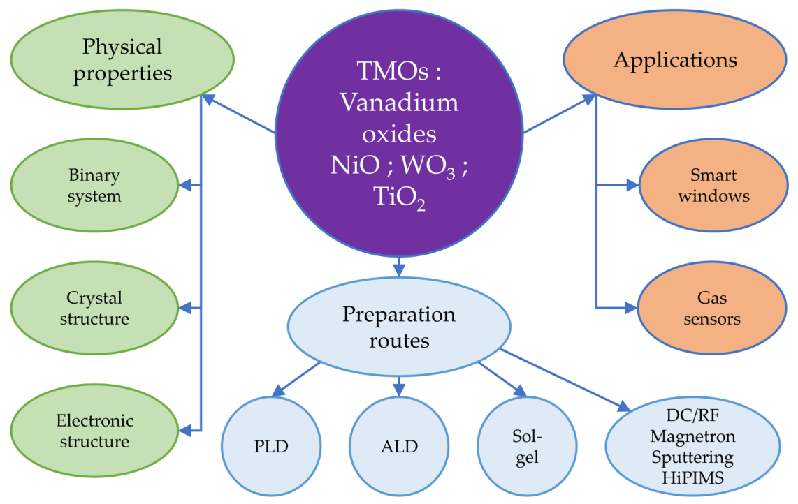
The article is organized into several major sections (Figure 2), each corresponding to a different level of analysis: the material platform section examines the structural and electronic proprieties of the selected TMOs; the technology section reviews the main preparation routes for TMO thin films; the applications section outlines the principal directions in which chromic properties of TMO thin films are utilized.

2. Materials Platform: Structural and Electronic Properties of Selected TMOs

2.1. Vanadium Oxides

2.1.1. V–O Binary Phase Diagram

The V–O phase diagram [19] reflects the thermodynamic equilibrium of phases over a wide temperature range and illustrates the complex phase relations that arise from the ability of vanadium to form oxides with different stoichiometries, oxidation states, and structural modifications. Despite the large number of phases shown in the diagram, the number of thermodynamically stable stoichiometric compounds is limited, whereas a significant fraction of the observed phases corresponds to solid-solution regions or metastable states. A characteristic feature of the V–O phase diagram is the presence of extended non-stoichiometric regions in both the V-rich and O-rich parts of the diagram. This behavior demonstrates the important role of oxygen content as a controlling parameter for phase stability in the V–O system.
In the V-rich region of the V–O phase diagram, four oxygen-containing solid solutions can be distinguished: α -, β -, γ -, and δ -V phases [20]. In the oxide region, five stoichiometric vanadium oxides are thermodynamically stable: V2O3 with a corundum-type trigonal structure ( R 3 ¯ c , No. 167), V3O5 with a monoclinic structure ( P 2 / c , No. 13), high-temperature rutile-type VO2 with a tetragonal structure ( P 4 2 / m n m , No. 136), V3 O 7 with a monoclinic structure ( C 2 / c , No. 15), and V2O5 with an orthorhombic structure ( P m m n , No. 59).
In addition to these stable stoichiometric compounds, the V–O system contains metastable and non-stoichiometric oxides that are typically formed under non-equilibrium, oxygen-deficient, or oxygen-rich conditions. Oxygen-deficient compositions are associated with mixed-valence Magnéli phases compositionally located between V2O3 and VO2, whereas oxygen-rich compositions are associated with Wadsley phases located between VO2 and V2O5. These homologous series describe how the V–O system accommodates oxygen deficiency or excess and can be represented as formal combinations of neighboring stable oxides.
The Magnéli phases are mixed-valence systems in which V3+ and V4+ ions coexist, and the average oxidation state of vanadium increases with increasing n. Their key structural feature is the presence of crystallographic shear planes, which arise from ordered shear transformations of the rutile-like VO6 octahedral framework. The resulting disruptions of the VO6 octahedral chains are accommodated by collective shifts of the octahedra, forming periodic shear planes whose spacing is determined by the parameter n:
V n O 2 n 1 = V 2 O 3 + ( n 2 ) VO 2 , 3 n 9 .
The Wadsley phases occupy the oxygen-rich side of the V–O phase diagram and can be represented as linear combinations of VO2 and V2O5:
V n O 2 n + 1 = V 2 O 5 + ( n 2 ) VO 2 , n 3 .
The Wadsley phases are likewise mixed-valence systems involving V4+ and V5+ ions. Unlike Magnéli phases, in which oxygen deficiency is accommodated by crystallographic shear planes, excess oxygen in Wadsley phases is accommodated through rearrangements of the octahedral framework and the formation of more complex layered or block-like structures. Their periodicity and connectivity are governed by the structural parameter n.

2.1.2. Crystal Structure of Vanadium Dioxide VO2

Below the MIT temperature, T c 68 ° C , VO2 exhibits insulating behavior and adopts a monoclinic structure. The M1 phase is the thermodynamically stable low-temperature phase of stoichiometric VO2, whereas the M2 phase is metastable and can be stabilized by applied stress, chemical doping, or epitaxial strain.
The M1 phase has the monoclinic space group P 2 1 / c (No. 14) and represents the stable low-temperature stoichiometric phase under ambient pressure. Its lattice parameters are a M 1 = 5.751 Å , b M 1 = 4.537 Å , c M 1 = 5.382 Å , α = γ = 90 , and β M 1 = 122 . 64 [21].
Structurally, the M1 phase is characterized by complete V–V dimerization along chains derived from the rutile c R direction. Each vanadium atom participates in the formation of V–V dimers, leading to a doubling of the unit cell and a lowering of the lattice symmetry relative to the high-temperature rutile phase. In addition to dimerization, the vanadium atoms undergo lateral displacements accompanied by rotations of the surrounding VO6 octahedra. These distortions break the equivalence of oxygen sites and result in two crystallographically distinct oxygen positions. The M1 structure therefore reflects a cooperative lattice distortion involving both V–V pairing and octahedral tilting, which plays a central role in stabilizing the insulating state of VO2 below T c .
The M2 phase is a metastable monoclinic phase with the space group C 2 / m (No. 12). Its lattice parameters are a M 2 = 9.066 Å , b M 2 = 5.797 Å , c M 2 = 4.525 Å , α = γ = 90 , and β M 2 = 91 . 88 [22].
Unlike the M1 phase, the M2 phase is not generally observed in bulk stoichiometric VO2 under ambient conditions but can be stabilized by chemical doping, applied stress, or epitaxial strain [22,23]. A defining feature of the M2 phase is the inequivalent behavior of vanadium chains. In this structure, only half of the vanadium chains exhibit V–V dimerization, while the remaining chains retain a non-dimerized configuration.
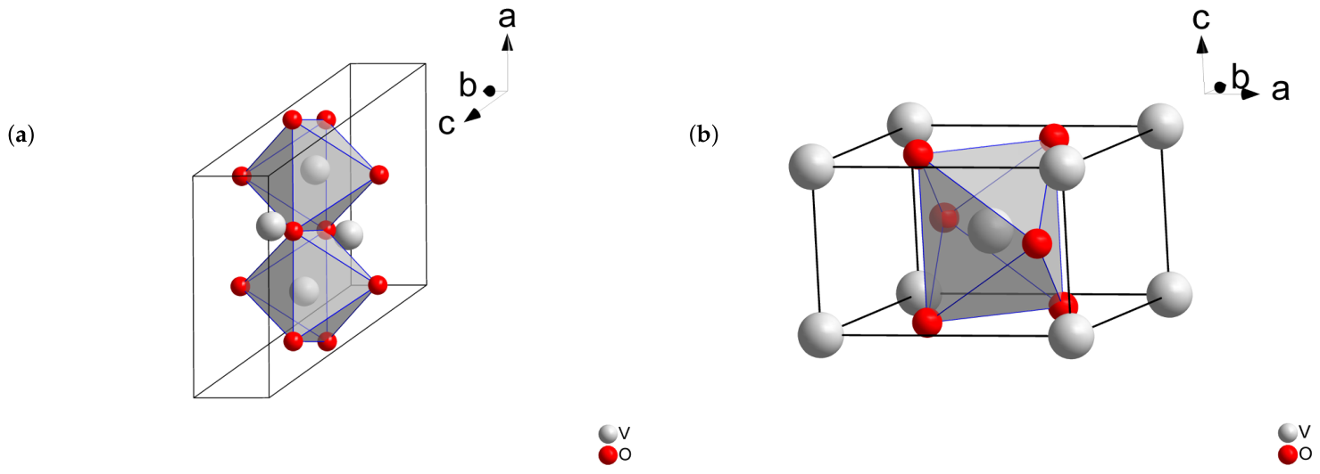
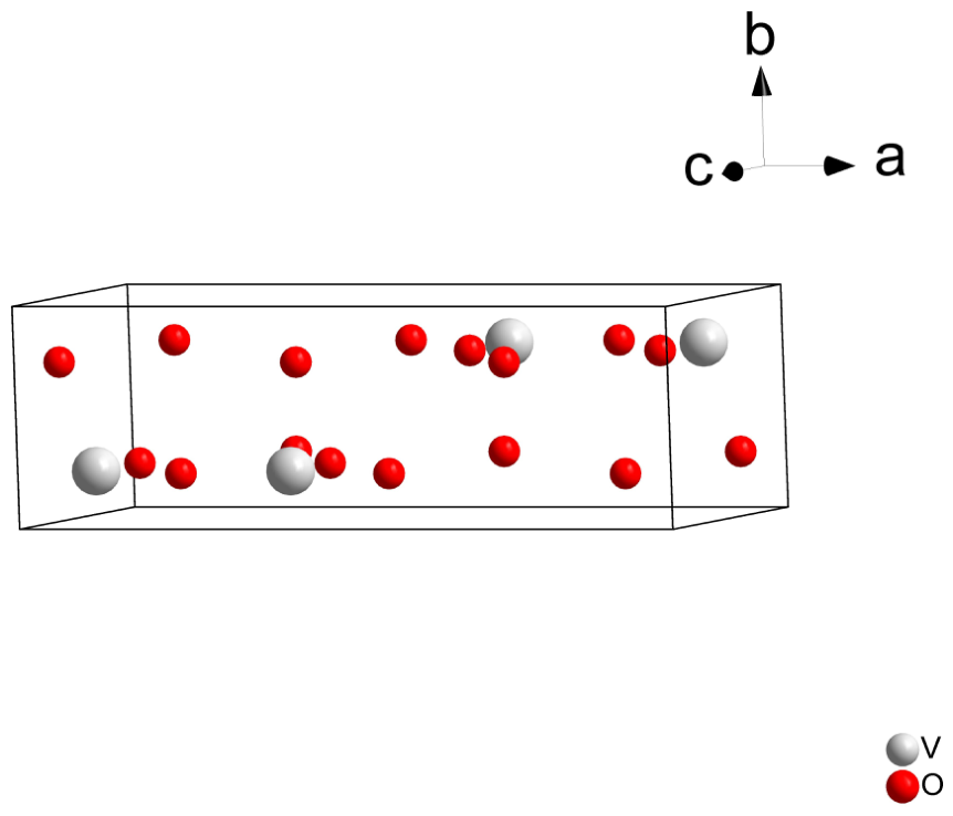
In the M1 phase, vanadium atoms and the two crystallographically distinct oxygen atoms occupy the Wyckoff position 4e. The corresponding symmetry-equivalent positions are given by ± ( x ; y ; z ) and ± ( x ; 1 / 2 y ; 1 / 2 + z ) . The fractional atomic coordinates are summarized in Table 1. Based on these atomic parameters, the crystal structure of VO2 is shown in Figure 3a.
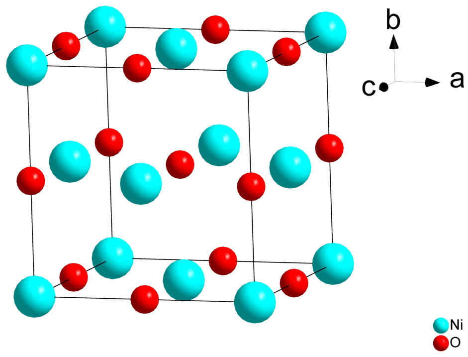
All crystal structure figures were generated using Diamond 4 software, based on crystallographic data reported in the corresponding cited references.
Above T c , VO2 transforms into a metallic phase with the rutile crystal structure. This high-temperature phase crystallizes in the tetragonal space group P 4 2 / m n m (No. 136). Its lattice parameters are a R = b R = 4.556 Å , c R = 2.860 Å , and α = β = γ = 90 [22] (Table 2, Figure 3b).
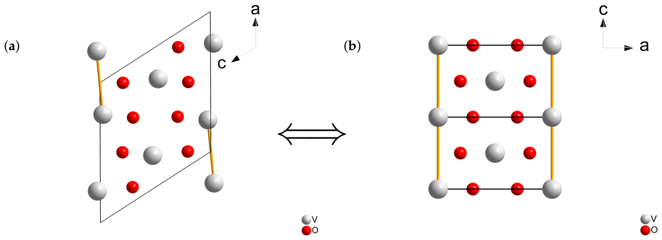
Across the MIT at T c , neighboring vanadium atoms within each chain shift toward one another, leading to V–V pairing, while the surrounding VO6 octahedra undergo accompanying rotations. This cooperative distortion produces a quasi-one-dimensional Peierls-like instability with contributions from electron correlations. It breaks the uniformity of the V chains, creates two distinct oxygen sites, and lowers the lattice symmetry from the rutile R phase to the monoclinic M1 phase.
The V–V distances become alternating, with a dimer bond length of 2.62 Å and an interdimer separation of 3.12 Å . Upon heating, this distortion is reversed and the structure transforms back into the rutile phase [24] (Figure 4); this process is reversible.

2.1.3. Crystal Structure of Divanadium Trioxide V2O3

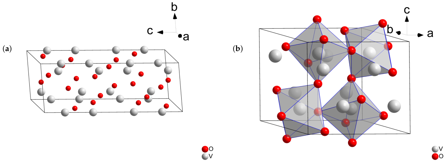
V2O3 is a strongly correlated TMO that exhibits an MIT accompanied by a structural phase transformation at T c 155 K . At higher temperatures, it adopts a corundum-type structure R 3 ¯ c (No. 167) with lattice parameters a = b = 4.951 Å , c = 14.003 Å , α = β = 90 , and γ = 120 [25] (Table 3, Figure 5a).
In this phase, all vanadium atoms are crystallographically equivalent and are octahedrally coordinated by oxygen, forming a three-dimensional lattice of edge-sharing VO6 octahedra. This high-symmetry structure corresponds to the metallic state of V2O3.
Upon cooling below T c , V2O3 undergoes a structural transformation into a monoclinic insulating phase with space group I 2 / a (No. 15) and lattice parameters a = 7.274 Å , b = 5.005 Å , c = 5.551 Å , α = γ = 90 , and β = 96 . 78 [26] (Table 4, Figure 5b). The monoclinic distortion lifts the equivalence of the vanadium sites and introduces subtle rearrangements of the VO6 octahedra, which are closely associated with the onset of electronic localization in the insulating state.

2.1.4. Crystal Structure of Divanadium Pentoxide V2O5

V2O5 represents the most oxygen-rich compound and the highest oxidation state phase in the V–O system, with vanadium in the formal V5+ ( d 0 ) electronic configuration. In contrast to VO2 and V2O3, V2O5 does not exhibit an MIT and remains insulating over a wide temperature range.
V2O5 crystallizes in an orthorhombic structure with space group P m m n (No. 59) and lattice parameters a = 11.512 Å , b = 3.564 Å , c = 4.368 Å , α = β = γ = 90 [27] (Table 5, Figure 6). The crystal structure is highly anisotropic and consists of layers formed by distorted VO5 square pyramids sharing edges and corners.

2.1.5. Electronic Structure of Vanadium Dioxide VO2

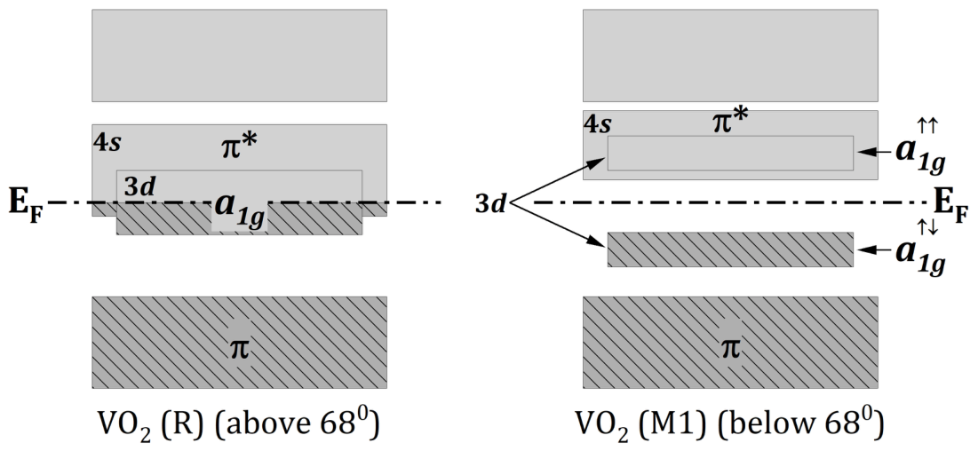
Vanadium dioxide (VO2) is a correlated oxide in which the electronic structure undergoes a pronounced reconstruction across the coupled structural–electronic MIT [28,29,30]. In VO2, vanadium is formally in the V4+ state with a 3 d 1 configuration; therefore, the electronic states near the Fermi level are governed primarily by V- 3 d states hybridized with O- 2 p states [24,31].
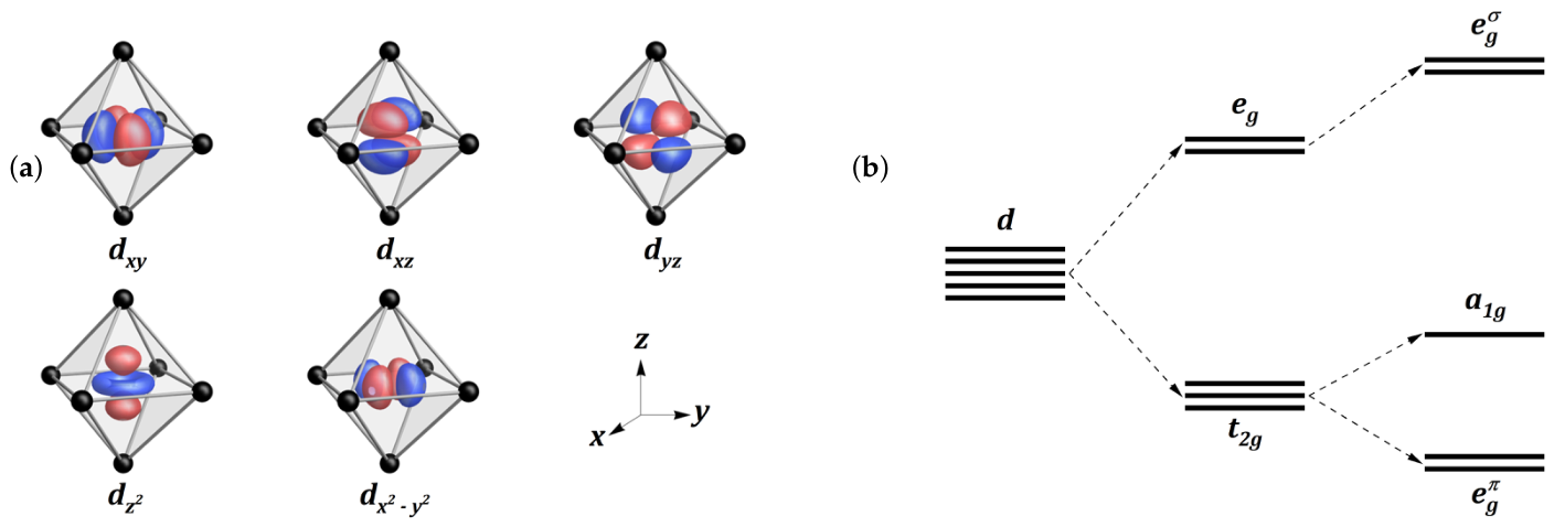
In an approximately octahedral VO6 environment, the five V- 3 d orbitals are split by the crystal field into a low-energy t 2 g manifold ( d x y , d x z , d y z ) and a high-energy e g manifold ( d z 2 , d x 2 y 2 ), with a characteristic splitting energy Δ O (occasionally denoted 10 D q ) (Figure 7a). Since the system hosts a single d electron, the t 2 g states primarily govern the electrical conductivity and the low-energy optical response. The actual local symmetry in VO2 deviates from the ideal O h symmetry; therefore, the t 2 g manifold further splits into sublevels: a 1 g , a singlet often denoted d , with the largest projection along the rutile axis c R and strong overlap along the V–V chains; and e g π , a doublet consisting of two orbital components with a smaller projection along c R and predominantly π -type overlap with O- 2 p states (pd π hybridization) [24,31,32] (Figure 7b).
In the high-temperature rutile phase, V atoms form quasi-linear chains along the c R axis. The a 1 g orbital exhibits the largest overlap along the V–V chains and gives rise to a relatively dispersive band, whereas the two e g π components hybridize more strongly with the oxygen 2 p states via π -channels. As a result, the t 2 g bands are partially filled, the Fermi level crosses the V– 3 d states, and the system exhibits metallic behavior. Importantly, the metallic state of VO 2 is correlated: the effective masses and spectral characteristics of quasiparticles differ markedly from the predictions of a simple single-electron picture due to substantial Coulomb correlations [29,30] (Figure 8). Upon lowering the temperature, VO2 transforms into the monoclinic M1 phase, accompanied by two key lattice distortions: dimerization of V atoms along the chains and tilting of the VO6 octahedra. Dimerization splits the a 1 g band into bonding and antibonding components due to the enhanced V–V overlap along c R . Simultaneously, octahedral tilting modifies the p d hybridization and the energetic position of the e g π states, typically shifting them upward relative to the Fermi level. As a result, the single d-electron occupies the lower a 1 g subband, while the upper a 1 g component and the e g π states lie at higher energies, leading to the opening of a band gap and insulating behavior [24,29,31,32] (Figure 8).

2.1.6. Electronic Structure of Divanadium Trioxide V2O3

Unlike VO2, where the MIT is strongly intertwined with a pronounced dimerization-driven band rearrangement, the MIT in V2O3 is commonly described as a Mott–Hubbard-type transition [33]. In stoichiometric V2O3, vanadium is formally in the V3+ state with a 3 d 2 configuration. Vanadium ions are coordinated by oxygen in an approximately octahedral VO6 environment, so the V- 3 d states are split by the crystal field into a low-energy t 2 g manifold and a high-energy e g manifold, separated by Δ O . Because the relevant d electrons primarily occupy the t 2 g region, the low-energy electronic structure near the Fermi level is dominated by t 2 g -derived states hybridized with O- 2 p states.
In the corundum structure, the local symmetry deviates from ideal O h symmetry due to a trigonal distortion of the VO6 octahedra, which further splits the t 2 g manifold into an a 1 g singlet and an e g π doublet. This trigonal splitting and the resulting orbital polarization ( a 1 g vs. e g π ) play an important role in shaping the low-energy spectrum and the MIT [34,35,36].
In the paramagnetic metallic (PM) regime, realized, for example, at elevated temperatures or under conditions that effectively increase the electronic bandwidth W, the t 2 g -derived bands are partially filled and the Fermi level crosses V- 3 d states, yielding metallic transport. However, the metallic phase is strongly correlated: quasiparticle bands are substantially renormalized, with reduced bandwidth and enhanced effective masses, and the spectral function typically exhibits reduced coherent weight near E F , accompanied by incoherent features at higher binding energies associated with Hubbard physics [37,38].
Upon entering an insulating regime, e.g., the antiferromagnetic insulating (AFI) phase at lower temperatures for stoichiometric material or a paramagnetic insulating state under specific tuning, the coherent spectral weight at the Fermi level is strongly suppressed and a gap opens. In the Mott–Hubbard representation, this corresponds to a redistribution of spectral weight from a coherent quasiparticle peak into lower and upper Hubbard bands, driven by the dominance of the on-site Coulomb repulsion U over the effective bandwidth W. The trigonal crystal-field splitting and orbital occupancy of the a 1 g and e g π submanifolds can influence the detailed character of the transition, including the degree of orbital selectivity and the magnitude of the gap [33,36,37,38].

2.1.7. Electronic Structure of Divanadium Pentoxide V2O5

Stoichiometric V2O5 is an insulating, charge-transfer (CT) TMO. Vanadium in V2O5 is formally in the V5+ oxidation state with a 3 d 0 electronic configuration, i.e., the V- 3 d shell is empty and there are no intrinsic carriers in a partially filled d band. The valence-band maximum is dominated by O- 2 p states, whereas the conduction-band minimum has predominantly V- 3 d character with substantial O- 2 p /V- 3 d hybridization; therefore, the Fermi level lies inside the band gap [39,40,41]. The stable ambient-pressure phase of V2O5 is orthorhombic and layered [27,42]. The V- 3 d states may still be approximately separated into t 2 g -like and e g -like groups. However, the low local symmetry and pronounced structural distortions substantially lift the degeneracy and modify the orbital energies compared with an ideal O h octahedron [39,42]. Unlike VO2 and V2O3, V2O5 is not characterized by a temperature-driven MIT under ambient conditions [43].

2.2. Nickel Oxide

2.2.1. Ni–O Binary Phase Diagram

In the Ni–O system [44,45], nickel oxide NiO is the only oxide that remains thermodynamically stable over a wide range of temperatures and oxygen partial pressures, whereas other nickel oxides appear only under restricted conditions and are generally metastable, such as Ni3O4, Ni3O3 and NiO2 [46]. Although the phase diagram indicates a strict Ni:O ratio of 1:1, in practice NiO almost always exists as a nickel-deficient oxide of the form Ni 1 x O ( x 10 3 10 1 ). Charge compensation in these non-stoichiometric states occurs through the formation of nickel vacancies, the presence of Ni3+ ions [47], and the emergence of localized hole polarons, which govern the p-type conductivity and significantly affect the optical properties of the material.

2.2.2. Crystal Structure of Nickel Oxide

Stoichiometric NiO crystallizes in the rock-salt structure, belonging to the space group F m 3 ¯ m (No. 225). The lattice parameter of the cubic unit cell is a = 4.177 Å [48] (Table 6, Figure 9). Each Ni 2 + ion is octahedrally coordinated by six O 2 ions, forming NiO6 octahedra, while each oxygen atom is similarly coordinated by six nickel ions.

2.2.3. Electronic Structure of Nickel Oxide

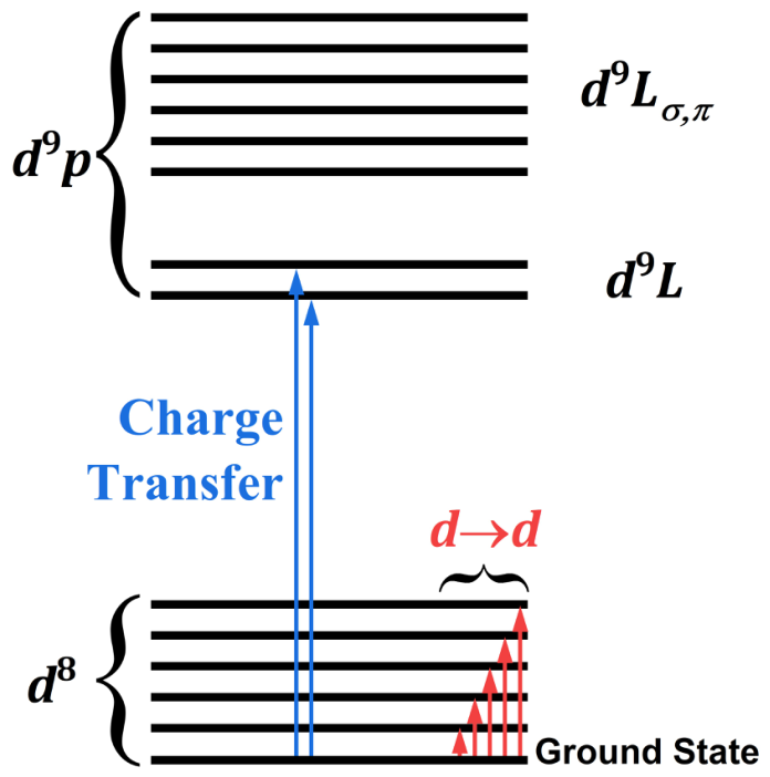
NiO is a prototypical strongly correlated TMO and a CT insulator. In stoichiometric NiO, nickel is formally Ni 2 + with a 3 d 8 configuration. In an approximately octahedral NiO6 environment, the Ni- 3 d states can be described by crystal-field splitting into t 2 g and e g components. However, the insulating gap is not captured by a simple one-electron crystal-field picture and instead reflects substantial electron–electron correlations and strong p d hybridization [49]. The valence states near the band edge contain a significant O- 2 p contribution hybridized with Ni- 3 d , while the unoccupied states have strong Ni- 3 d character [50] (Figure 10).

2.3. Tungsten Oxides

2.3.1. W–O Binary Phase Diagram

The W–O system [51] exhibits one of the most complex phase diagrams among TMOs, characterized by a large number of reported oxide phases spanning a narrow range of oxygen concentrations. This apparent complexity does not arise from the stabilization of numerous independent stoichiometric compounds, but rather from the formation of extended families of structurally related oxygen-deficient and oxygen-rich phases derived from the WO3 framework.
In the O-rich region of the W–O phase diagram, the thermodynamic stability is restricted to a limited number of oxide phases. The only fully stoichiometric and widely stable oxides are WO2 and WO3, which define the lower and upper bounds of oxygen content in this region. Between these two phases, a series of intermediate oxygen-deficient tungsten oxides is stabilized. These phases represent extended homologous series derived from the WO3 framework via crystallographic shear mechanisms.

2.3.2. Crystal Structure of Tungsten Oxide WO3

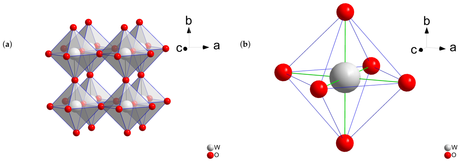
All polymorphs of WO3 can be viewed as distortions of the cubic ReO 3 -type structure P m 3 ¯ m (No. 221) (Table 7, Figure 11a), which consists of a three-dimensional framework of corner-sharing WO6 octahedra (Figure 11b).
The ideal cubic WO3 structure is metastable and can be stabilized only under non-equilibrium conditions, such as chemical substitution or lattice constraint effects, since the A-site of the perovskite lattice remains vacant. Structural polymorphism in WO3 arises primarily from cooperative tilting of WO6 octahedra and off-centering of W atoms within the octahedral units [52]. As a result, WO3 undergoes a sequence of symmetry-lowering phase transitions with decreasing temperature, exhibiting several stable crystallographic phases over the temperature range from 0 to 1170 K (Table 8).

2.3.3. Electronic Structure of Tungsten Oxide WO3

Tungsten trioxide WO3 in stoichiometric form is a d 0 oxide: tungsten is formally in W6+ oxidation state with a 5 d 0 electronic configuration, so the conduction band is derived primarily from empty W- 5 d states, whereas the valence band is dominated mainly by O- 2 p states with significant hybridization [58,59]. In an octahedral environment, the low-lying W-d conduction states are often predominantly t 2 g -like, but real structures exhibit sizable distortions that lift degeneracies and modify the band dispersion [60]. WO3 exhibits multiple temperature-dependent polymorphs, yet it is generally treated as a semiconductor/insulator in its stoichiometric forms; the key changes are typically in lattice symmetry and quantitative band-edge positions rather than a temperature-driven MIT as in VO 2 [58,60].

2.4. Titanium Oxides

2.4.1. Ti–O Binary Phase Diagram

The Ti–O system can be regarded as an intermediate case among TMOs, combining a relatively high solubility of oxygen in metallic titanium with the formation of numerous non-stoichiometric and shear-structure oxides at increasing oxygen content [61,62].
At intermediate oxygen concentrations, the Ti–O system is dominated by titanium suboxides based on TiO and Ti 1 x O compositions. The nominal TiO phase crystallizes in a NaCl-type B1 structure and exhibits an exceptionally wide range of non-stoichiometry, which is accommodated by the simultaneous presence of vacancies on both the titanium and oxygen sublattices. As a result, TiO cannot be regarded as a strictly stoichiometric compound, but rather as a defect-stabilized phase with variable composition. Depending on temperature and oxygen chemical potential, TiO-based phases may undergo vacancy ordering, giving rise to lower-symmetry structures such as α -TiO and β -TiO. These suboxides typically exhibit metallic or semimetallic conductivity and represent a transitional regime between metallic solid solutions and oxygen-rich shear-structure oxides. In addition to the nominal TiO composition, the Ti–O system contains several titanium suboxides in the Ti-rich and intermediate oxygen concentration range. Early suboxides such as Ti3O, Ti2O, and Ti3O2 are typically interpreted as oxygen-ordered derivatives of metallic titanium rather than distinct stoichiometric oxides.
In the O-rich region of the Ti–O system, phase stability is governed by stoichiometric titanium dioxide TiO2 and a series of ordered oxygen-deficient Magnéli phases. The O-rich phases are stabilized by well-defined crystallographic rearrangements of the TiO6 octahedral framework.
TiO2 represents the fully oxidized and strictly stoichiometric endpoint of the Ti–O system. It is thermodynamically stable over a wide range of temperatures and oxygen partial pressures and crystallizes in several polymorphic modifications, with the rutile structure being the most stable under ambient conditions. All Ti sites in TiO2 are occupied by Ti4+ ions in octahedral coordination, and large deviations from stoichiometry are energetically unfavorable.
Between TiO and TiO2, a series of Magnéli phases with the general formula Ti n O 2 n 1 forms a distinct homologous series. These compounds are thermodynamically stable phases rather than defect variants of TiO2 and are characterized by the presence of periodic crystallographic shear planes within a rutile-derived structure. The introduction of shear planes accommodates oxygen deficiency without the formation of isolated point defects, resulting in well-defined compositions and long-range structural order. The Magnéli phases exhibit mixed-valence titanium states, Ti3+/Ti4+, and display electronic properties ranging from semiconducting to metallic, reflecting the progressive reduction of TiO2. Structurally and electronically, they constitute a transitional regime between corundum-type Ti2O3 and rutile TiO2, playing a central role in the O-rich phase chemistry of titanium oxides.

2.4.2. Crystal Structure of Titanium Oxide TiO 2

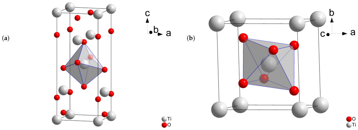
TiO2 crystallizes in three main polymorphic phases: anatase, rutile, and brookite. Anatase adopts a tetragonal structure with space group I 4 1 / a m d (No. 141) and lattice parameters a = b = 3.784 Å and c = 9.514 Å [63] (Table 9, Figure 12a). Rutile crystallizes in the tetragonal space group P 4 2 / m n m (No. 136) with lattice parameters a = b = 4.594 Å and c = 2.959 Å [64] (Table 10, Figure 12b), while brookite exhibits an orthorhombic structure belonging to space group P b c a (No. 61) [65,66]. Among these polymorphs, rutile is the thermodynamically stable phase under ambient conditions, whereas anatase and brookite are metastable and can be stabilized depending on synthesis conditions, particle size, and strain.
All polymorphs of TiO2 are constructed from TiO6 octahedra, in which Ti4+ ions are octahedrally coordinated by six O 2 ions. The different crystal structures arise from variations in the connectivity, distortion, and tilting of these octahedra. In the rutile structure, TiO6 octahedra share edges along the crystallographic c-axis and corners in the perpendicular directions, forming a relatively dense and compact framework. In contrast, anatase exhibits a more open structure with stronger octahedral distortions, which is often associated with enhanced surface reactivity and a higher propensity for defect formation.

2.4.3. Electronic Structure of Titanium Oxide

Titanium dioxide (TiO2) is also a prototypical d 0 oxide: titanium is formally in the Ti4+ oxidation state with a 3 d 0 electronic configuration. The electronic structure is therefore dominated by O- 2 p states at the top of the valence band and Ti- 3 d states at the bottom of the conduction band. In the approximately octahedral TiO6 environment, the Ti- 3 d states are split into lower-energy t 2 g -like and higher-energy e g -like groups, although the actual splitting depends on the polymorph, rutile, anatase, or brookite, and on local structural distortions [67,68]. The best-known polymorphs, rutile and anatase, have similar orbital character but differ in quantitative band-structure details, such as band-gap magnitude and band dispersion. For many optical and photochemical effects, a key role is often attributed to oxygen vacancies and related Ti3+-associated gap states; modern electronic-structure studies describe their electronic levels using beyond-semilocal DFT approaches, such as hybrid functionals [69].

2.5. Comparative Summary of Selected TMOs

Table 11 summarizes the key properties and chromic responses of the selected TMOs, providing the direct comparison between vanadium, nickel, tungsten and titanium oxides.

3. Technology of TMO Preparation

3.1. Pulsed Laser Deposition

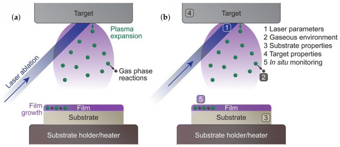
Pulsed laser deposition (PLD) is a physical vapor deposition technique in which a high-power pulsed laser ablates a solid target inside a vacuum chamber, producing a plasma plume that expands toward a substrate where the ablated species condense. The process can be regarded as a sequence of strongly coupled stages: laser–target interaction and ablation, plume formation and expansion, including scattering and gas-phase reactions, and subsequent nucleation and growth on the substrate surface. As a result, the film thickness, microstructure, crystallinity, and phase stability can be tailored by adjusting the laser fluence, repetition rate, substrate temperature, target–substrate distance, and background gas pressure [70,71]. For TMO films, the oxygen background is particularly critical: plume–gas collisions and reactions can promote the formation of oxide species and precursors, enhance oxygen incorporation, and reduce the kinetic energy of arriving species, thereby mitigating surface damage and helping to stabilize the desired phase. In addition, oxygen pressure represents an effective processing parameter for tuning oxygen-related defect populations, such as oxygen vacancies, and consequently the functional properties of the grown oxide [72,73,74].
A schematic representation of the key PLD processes and main control parameters is shown in Figure 13, while representative deposition conditions for selected TMOs are summarized in Table 12.
A major reason why PLD is widely used for the growth of TMO thin films is its combination of versatility and compositional control. Many complex oxides can be deposited from a single target with the desired composition, and PLD often enables near-stoichiometric transfer because the ablation and transport processes are highly energetic and occur on short time scales. However, deviations between the target and film composition may still occur due to incongruent ablation, preferential scattering in the background gas, and re-sputtering, particularly when the background pressure and kinetic energy of the plume species vary [89]. The energetic, ionized plume can also assist crystalline growth and, in some cases, reduce the substrate temperature required for crystalline or epitaxial film formation. The setup is comparatively clean and convenient for multilayer structures, since different targets can be switched during the same deposition run while the laser source remains outside the chamber [72,73].
At the same time, PLD has well-known limitations that are relevant to practical TMO devices. The plume is typically forward-directed and has a limited cross-sectional area, partly determined by the laser spot size, which complicates thickness uniformity and scaling to large-area substrates. For the same geometrical reason, conformal step coverage and in situ thickness control can also be challenging. Another persistent issue is the formation of droplets and particulates during ablation, which can be incorporated into the film surface and degrade performance or even cause device failure. Thus, PLD is often a method of choice for producing high-quality, compositionally faithful TMO films and multilayer structures, but it requires careful process optimization when thickness uniformity, droplet-free surfaces, and large-area manufacturing are required [71,90].
Overall, the representative deposition conditions summarized in Table 12 highlight the broad tunability of PLD for TMOs, where phase formation and defect populations can be adjusted by oxygen pressure, substrate temperature, and laser parameters. In oxide PLD, KrF excimer lasers ( λ = 248 nm ) are used most frequently, and the employed laser fluence is commonly in the 1– 2 J cm 2 range.

3.2. Magnetron Sputtering

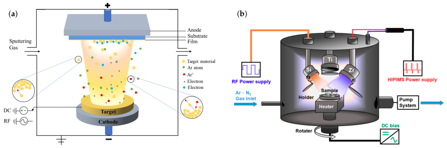
Reactive magnetron sputtering is a widely used physical vapor deposition technique for growing TMO thin films with good thickness uniformity and strong industrial scalability. A metallic or suboxide target is bombarded by ions from a plasma, most commonly sustained in argon, ejecting atoms and clusters from the target surface. These sputtered species are transported through the gas phase and condense on a substrate to form a thin film. In the magnetron configuration, a magnetic field near the target confines electrons, enhances ionization, and thereby enables a stable discharge at relatively low pressures and high deposition rates (often with reduced thermal load on the substrate compared to non-magnetron operation) [91,92].
To deposit oxides, O2 is introduced together with Ar, and the sputtered metal species react in the plasma and/or at the growing surface to form the oxide. Consequently, phase formation, stoichiometry, defect chemistry, and microstructure are governed by parameters such as total pressure, oxygen partial pressure (or O2 flow), Ar:O2 ratio, applied power (DC for conductive targets, RF for insulating conditions, and often pulsed-DC in reactive operation), substrate temperature, substrate bias, and the overall plasma composition. For many TMOs, oxygen partial pressure is especially critical because it directly affects oxygen vacancies and therefore electrical and optical properties [93,94].
One of the main advantages of reactive magnetron sputtering for TMO films is its ability to deliver uniformity and reproducibility over large areas. Thus, it is widely used for coatings and device fabrication. It is compatible with a broad range of substrates and can be operated at relatively low substrate temperatures. Multi-target sputtering and co-sputtering further enable composition tuning, doping, and multilayer architectures [93,95].
The method also has limitations. In reactive operation, the target surface can undergo oxidized target poisoning, reducing the deposition rate and introducing process hysteresis, which complicates stable control of oxygen incorporation—especially near the transition between metallic and compound modes [93,94,96].
In addition, because the typical kinetic energy of arriving species is lower than in highly energetic plume-based methods, high crystallinity in some TMOs may require elevated substrate temperatures, substrate biasing, or post-deposition annealing. Finally, plasma-driven ion bombardment can induce stress, cause re-sputtering of light elements, or create subsurface damage if pressure and bias conditions are not optimized. Overall, reactive magnetron sputtering is a robust and scalable route to functional TMO thin films, but it requires careful tuning of oxygen and plasma conditions when phase purity, defect engineering, and precise stoichiometry are critical [93,94]. Representative sputtering configurations (RF/DC reactive and HiPIMS) are summarized schematically in Figure 14, while representative growth conditions for selected TMOs are listed in Table 13.
Overall, Table 13 emphasizes the practical versatility of magnetron sputtering for TMO thin films. In most studies, oxide layers are deposited in reactive mode using either DC power, for conductive targets, or RF power, commonly adopted to maintain stable operation when the target surface becomes oxidized. A further advantage is the broad compatibility with substrates of different thermal and structural constraints, including glass and SLG for scalable coatings, together with single-crystal substrates, such as sapphire, when improved crystallinity or texture control is needed. Together with the possibility of multi-target sputtering and co-sputtering, these features make magnetron sputtering an established technique for large-area TMO coatings and device fabrication, where uniformity, reproducibility, and compositional and defect tuning through oxygen control are the primary requirements.

3.3. Sol-Gel and Aerosol Spray Deposition

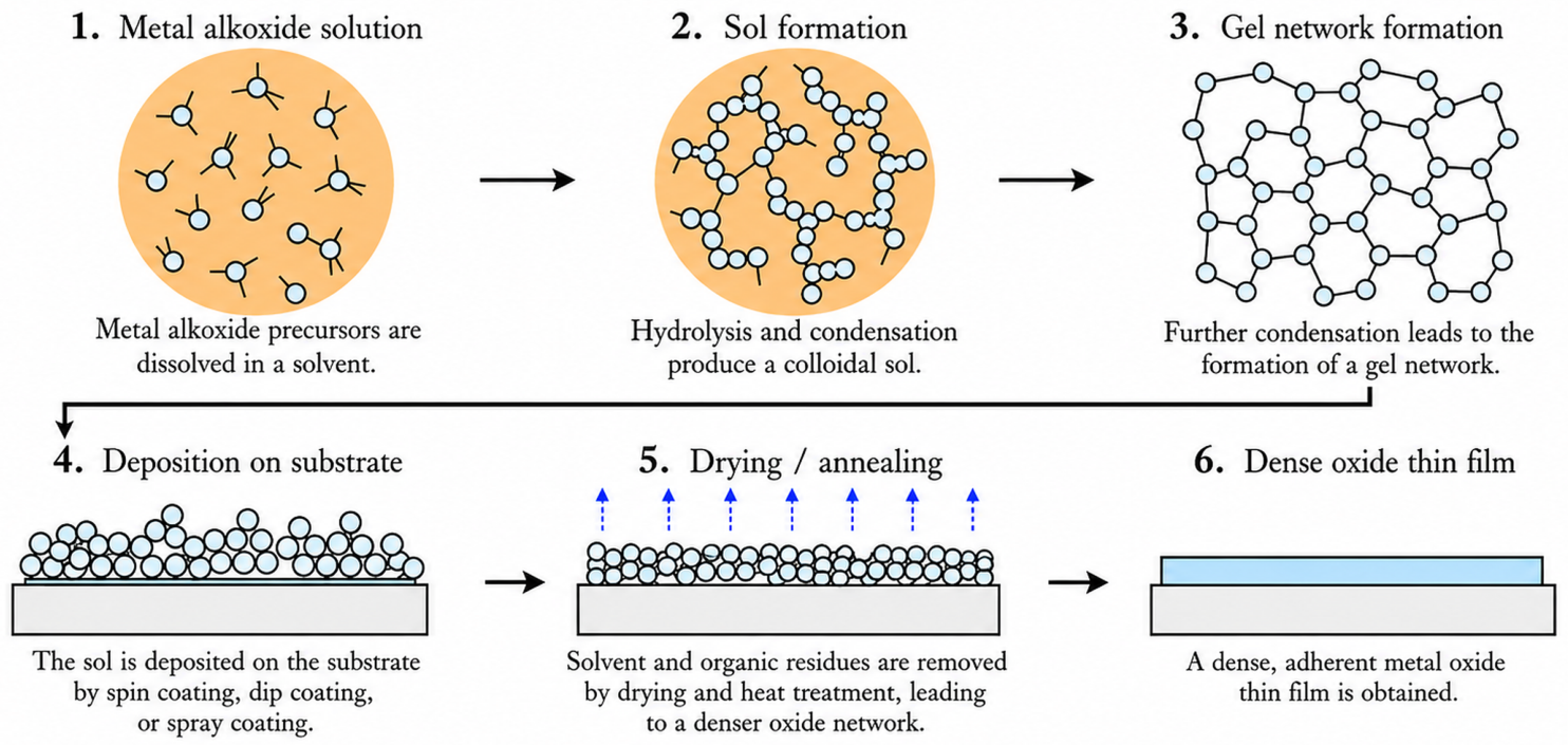
Sol–gel processing (Figure 15) is a solution-based chemical route for producing inorganic thin films and coatings, in which molecular precursors, commonly metal alkoxides or metal salts, are converted into an extended M–O–M network through hydrolysis and condensation reactions. The resulting colloidal sol evolves toward a gel, and subsequent drying and thermal treatment remove volatile species and organic residues, densify the layer, and, when required, promote crystallization of the final inorganic phase [112].
For thin film formation, the sol is typically deposited onto a substrate by dip-coating or spin-coating, with film thickness and uniformity governed by coupled fluid-dynamic and evaporation phenomena, including withdrawal or spin speed, viscosity, surface tension, and solvent volatility. At the same time, the developing gel network determines shrinkage, porosity, and mechanical integrity during drying. In practice, film properties are strongly influenced by chemical parameters, such as precursor type, solvent system, water-to-precursor ratio, pH, complexing or chelating agents, and aging time, together with processing parameters, including ambient humidity during drying, heating rate, annealing temperature, dwell time, and annealing atmosphere [113].
In aerosol-assisted variants, the precursor sol or solution is atomized into droplets and transported to the substrate, enabling coating of large areas and non-planar geometries and offering a practical pathway toward scalable manufacturing. Depending on temperature and chemistry, conversion to the final inorganic network can occur predominantly after deposition, as in aerosol-gel or aerosol-assisted sol–gel processing, or partially during flight, impact, and subsequent heating, as in spray-based routes [114,115,116]. Representative TMO thin film examples obtained using sol–gel routes and their processing conditions are summarized in Table 14.
Overall, Table 14 highlights the practical versatility of sol–gel processing for TMO thin films. Across the reported studies, spin coating and dip coating are the most common deposition modes, while a wide variety of substrates, including Si, quartz, glass, and transparent conductive glass such as ITO- or FTO-coated glass, can be employed depending on the targeted device architecture. The cited examples also illustrate that sol–gel chemistry provides multiple precursor options, including alkoxides, acetylacetonates, chlorides, and acetates, as well as straightforward composition tuning at the solution-processing stage. Importantly, the final oxide phase, crystallinity, and defect-related properties are largely determined by the drying and annealing steps, including atmosphere control, making thermal processing a central processing parameter for sol–gel prepared TMOs in functional coatings.

3.4. Other Deposition Methods

Beyond PLD, magnetron sputtering, and sol–gel, several other thin film technologies are frequently employed to access either (i) highly conformal coatings and precise thickness control, (ii) scalable conformal growth on complex geometries, or (iii) epitaxial films for fundamental structure–property studies. In the context of the present TMOs (VO2, WO3, TiO2, NiO), particularly relevant routes include atomic layer deposition (ALD), chemical vapor deposition (CVD, including aerosol-assisted CVD), electrochemical growth (electrodeposition/anodization), and molecular beam epitaxy (MBE).
Atomic layer deposition (ALD) is especially attractive when thickness control and conformality on textured or 3D substrates are required. VO2 films have been demonstrated by ALD using inorganic precursors, such as VCl 4 , with direct crystallization under suitable conditions [129]. NiO electrochromic coatings have also been prepared by ALD on transparent conductive substrates, illustrating the viability of ALD for anodic electrochromic oxides [130]. For WO3, ALD processes, such as W ( CO ) 6 + O 3 , have been reported as a route to controlled ultrathin tungsten oxide films [131]. TiO2 is one of the best-established ALD oxides; comprehensive reviews summarize its wide precursor chemistry and broad application space [132].
CVD and aerosol-assisted CVD (AACVD) methods are widely used for scalable oxide coatings, often providing good step coverage and industrial compatibility. Thermochromic VO2 films have been fabricated by low-pressure CVD (LPCVD), demonstrating controllable growth of crystalline VO2 from volatile vanadium precursors [133]. AACVD has been used to prepare doped VO2 films as well as WO3 coatings on glass from solution-deliverable precursors [134,135]. For NiO, metal–organic methods have been reported for electrochromic NiO coatings, highlighting that gas-phase chemistry can also be leveraged for this anodic electrochromic oxide [136].
Electrochemical methods, including electrodeposition and anodization, are particularly common for electrochromic TMOs because they naturally integrate with conductive substrates and can yield porous or high-surface-area morphologies. NiO electrochromic films have been produced by electrodeposition onto FTO-coated glass [136]. WO3 is likewise frequently prepared by electrodeposition for electrochromic applications, with multiple studies and reviews treating electrodeposition as a key low-cost method to obtain functional WO3 coatings [137]. For TiO2, anodization of Ti or Ti-coated substrates is a standard method to obtain self-organized TiO2 nanotube arrays, enabling strongly nanostructured films after subsequent annealing [138,139].
Molecular beam epitaxy (MBE), including oxide or oxygen-assisted variants, is often used when epitaxial, well-defined model films are needed to probe intrinsic mechanisms and substrate/strain effects. VO2 ultrathin films have been grown by reactive MBE on rutile TiO2 substrates [140]. Plasma-assisted MBE has also been applied to epitaxial NiO films on semiconducting substrates [141]. For WO3, single-crystalline and epitaxial WO3 thin films grown by MBE have been reported and used to study orientation-dependent functional behavior [142,143]. Epitaxial rutile TiO2 films on sapphire grown by MBE have been reported, illustrating MBE control over phase and microstructure [144].
Overall, other routes complement PLD, sputtering, and sol–gel processing by offering either superior conformality and thickness control (ALD), scalable conformal growth with strong industrial relevance (CVD/AACVD), device-friendly electrochemical fabrication of porous electrochromic layers (electrodeposition/anodization), or high-purity epitaxial model films for mechanistic studies (MBE).

3.5. Comparative Analysis of TMO Thin Film Preparation Technologies

The preparation route is a key factor that determines not only the phase composition, crystallinity, morphology, and stoichiometry of chromic TMO thin films, but also their technological relevance for practical devices. While laboratory-scale methods such as PLD and MBE are highly useful for obtaining well-controlled model systems and clarifying structure–property relationships, scalable techniques such as magnetron sputtering, sol–gel processing, spray deposition, ALD, CVD, and electrochemical deposition are more directly connected with device fabrication. Therefore, the choice of deposition method should be evaluated not only in terms of film quality, but also with respect to scalability, processing temperature, substrate compatibility, reproducibility, cost, and integration into multilayer or device architectures. A comparative overview of the main advantages, limitations, and device-integration aspects of the reviewed preparation technologies is summarized in Table 15.

4. Devices and Applications

4.1. Thermochromic VO2-Based Smart Windows

SWs are a critical component of the building envelope because they simultaneously manage (i) transmission heat losses driven by temperature differences, (ii) solar heat gains driven by short-wave irradiance, and (iii) daylight access, which affects both lighting energy demand and visual comfort.
In the energy balance of a building, the contribution of a window is commonly described by two main terms: a non-solar term, determined by the overall heat transfer coefficient (U-value), and a solar term, determined by the solar heat gain coefficient (SHGC, or g-value). At the same time, optical parameters such as visible transmittance ( T lum ) and solar transmittance ( T sol ) govern the quality of daylighting and solar-energy admission. Therefore, window performance is inherently multi-objective: a low U-value and an optimized SHGC are central design goals, but they must be balanced against daylight access, outside view, condensation resistance, and the long-term durability of the insulating glass unit (IGU) [145].
In more detailed analyses, the angular dependence of solar transmission and the spectral transmittance and reflectance over the solar spectrum are also taken into account. In typical double glazing with an air-filled cavity, a substantial part of the heat transfer across the gap may occur through long-wave radiative exchange between the panes, especially because uncoated glass has high thermal emittance. In addition, perimeter components such as spacers and edge seals may act as thermal bridges and strongly affect service life by limiting moisture ingress and fill-gas leakage. These edge-region effects are therefore not secondary: they directly influence the effective window-level U w and determine whether the initial thermal performance is maintained over time [146].
A conventional window is typically characterized by standardized performance parameters, including U 0.35 , SHGC 0.8 , T vis 0.9 , and T sol 0.8 .
A passive way to improve glazing performance is to combine low-emissivity (low-e) coatings with optimized cavity fills. Low-e coatings suppress long-wave radiative heat transfer by lowering the surface emissivity of the glazing, thereby reducing U g without necessarily sacrificing high visible transmittance T vis when spectrally selective designs are used. Reviews of commercially available low-e materials and products show that such coatings are already a widely implemented strategy for improving both the thermal and optical performance of windows [147]. In parallel, replacing air in the cavity with inert gases, most commonly Ar and, in higher-performance configurations, Kr, reduces conductive and convective heat transfer across the gap. However, the magnitude and long-term persistence of this benefit depend strongly on the quality of the edge seal and spacer design, since these components govern both gas retention and resistance to moisture ingress over service life [146].
An active way to further improve glazing performance beyond low-e coatings and gas fills includes triple glazing, warm-edge spacers, vacuum insulating glazing, and smart glazing technologies that dynamically tune solar and/or visible transmittance to match operational needs. Reviews show that electrochromic and related SWs can reduce cooling demand by modulating transmittance under external control. They can also lower lighting demand by maintaining a more favorable daylighting regime. In contrast, thermochromic systems, often based on VO2, provide passive, temperature-driven solar control. The physics and optimization of thermochromic performance, particularly the trade-off between solar modulation and luminous transmittance, have been extensively reviewed and experimentally characterized [148].
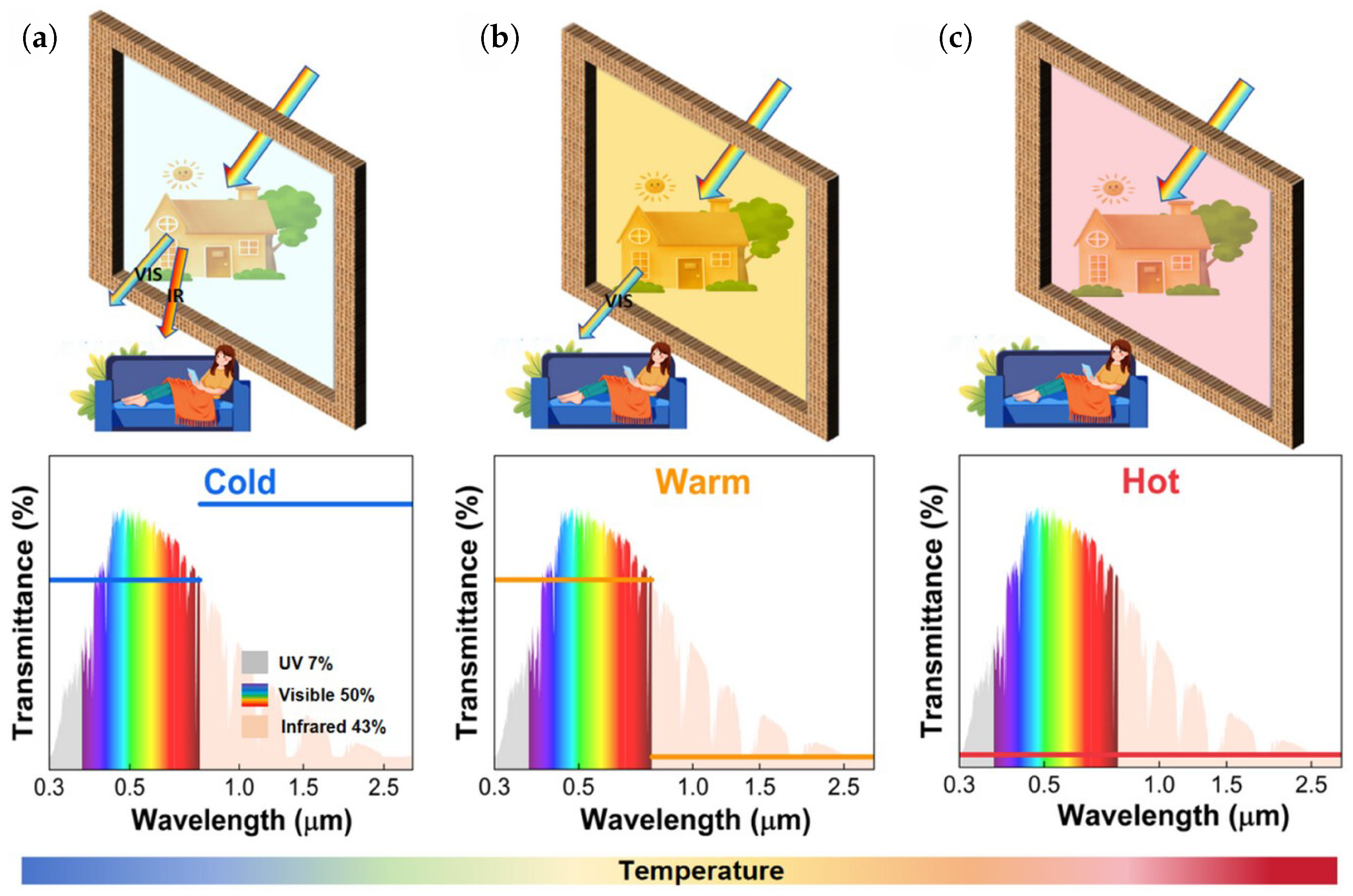
In summer, an ideal SW (Figure 16) should maintain a bright indoor environment while limiting solar heat gains. It should transmit most of the visible light, about 60–80% in the 380–780 nm range, to preserve daylighting and a clear outside view, while blocking or reflecting a significant portion of the near-infrared radiation, about 780–2500 nm, which is mainly responsible for solar heating. Thus, an SW should remain highly transparent in the visible range, suppress NIR transmission, and, ideally, facilitate net radiative heat rejection from the indoor side to the outdoor environment.
In winter, an ideal SW should maximize useful solar heat gains while minimizing heat losses. It should still maintain high visible transmittance, about 60– 80 % in the 380–780 nm range, to ensure daylight access, but it should also exhibit high solar transmittance over a broad part of the solar spectrum to support passive heating. In the long-wave infrared, the desirable behavior is generally the opposite of the summer case: the window should reduce radiative heat loss by reflecting thermal radiation emitted by indoor surfaces back into the room. Thus, the winter-optimal state combines good visible transparency and enhanced solar admission with improved retention of indoor thermal radiation.
The application of vanadium oxide in SW is limited by its intrinsic properties, namely relatively low luminous transmittance ( T lum 40 % ), relatively high absorption, and a limited solar modulation efficiency ( Δ T sol 10 % ) for a single layer. Moreover, the critical temperature ( T c 68 °C) is too high for most climatic regions. Therefore, lowering the critical temperature to T c 25 ° C and improving T lum are the main requirements for practical VO2-based SWs. Another challenge is the long-term cycling stability of VO2, since in the presence of oxygen it may undergo further oxidation to V2O5, which is the most stable oxidation state among vanadium oxides. These challenges can be addressed by doping, morphology engineering, and multilayer design.
Elemental doping is one of the conventional approaches used to tailor the MIT temperature and optical properties (Table 16). The choice of dopant is usually guided by two main considerations: increasing the carrier density to promote the electronic phase transition, or inducing lattice distortion to facilitate the structural phase transition [150].
Besides lowering T c , another major challenge for practical VO2-based SWs is to achieve sufficiently high luminous transmittance ( T lum ) together with adequate solar modulation ability ( Δ T sol ). One possible solution is related to the design and architecture of the glazing stack. A VO2-based SW typically consists of a multilayer thin film structure, as shown in Figure 17. To reduce optical reflection losses and increase luminous transmittance, additional antireflection (AR) layers may be incorporated into the structure (Figure 17d). Candidate AR materials are listed in Table 17 and can be selected depending on the target optical and functional requirements of the device. The optimum thickness and the appropriate refractive index of these layers can be evaluated by means of the transfer matrix method (TMM), which is widely used for the optical design and optimization of multilayer coatings. Thus, multilayer engineering and the integration of AR coatings provide an effective route for improving the optical performance of VO2-based methods.
Thus, a practical route toward high-performance thermochromic glazing is obtained by combining two complementary optimization strategies: chemical tuning of the active VO2 by doping and optical tuning of the complete coating stack by AR, buffer, and protective layers. Doping mainly controls the intrinsic thermochromic response of VO2, especially the T c , visible absorption, and NIR modulation, whereas AR and buffer layers control reflection losses, optical interference, crystallization, interfacial strain, and long-term stability. Therefore, the most successful VO2-based SW coatings are multilayer structures in which composition, thickness, morphology, refractive-index, and interface quality are optimized simultaneously [164,165,166].
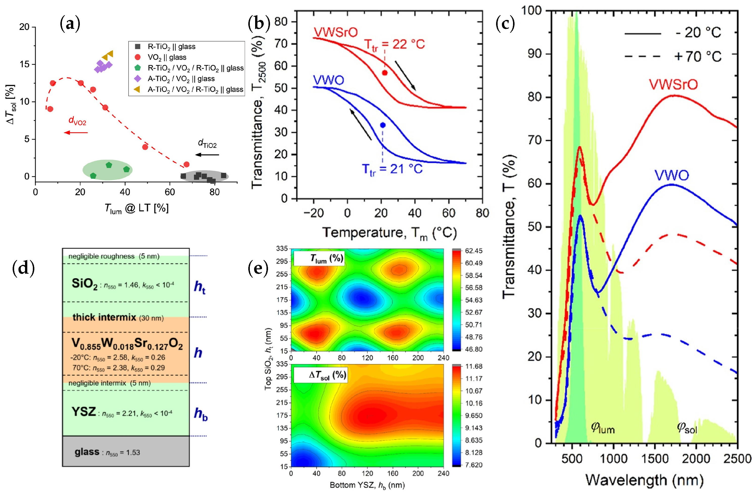
Becker et al. [164] investigated the role of TiO2 AR and buffer layer in undoped VO2 film in order to separate the effect of optical multilayer engineering from doping of the VO2 layer. The choice of TiO2 is motivated by the following considerations. Rutile TiO2 is structurally compatible with the high-temperature rutile phase of VO2 and can therefore promote the formation of the desired thermochromic phase, whereas TiO2 top layers can act as AR coatings for reducing reflection losses and increasing T lum . In this concept, the bottom rutile TiO2 layer acts mainly as a buffer layer, while the top anatase TiO2 layer acts as an AR layer. The coating was prepared by ion-beam sputter deposition (IBSD) on quartz glass, using a customized ceramic TiO2 target for the deposition of both rutile and anatase TiO2 layers and a metallic V target with a purity of 99.9 % for the VO2 layer. This technique was selected because it allows the sequential deposition of oxide thin films under controlled energetic ion bombardment, which is important for stabilizing the desired TiO2 and VO2 phases and for controlling the morphology and interface quality of the multilayer stack. In the first step, R-TiO2, VO2, and VO2/R-TiO2 films were deposited on quartz glass at 550 ° C, providing the reference structures required to evaluate the influence of the rutile TiO2 buffer layer on the growth and thermochromic response of VO2. The optical constants, namely the refractive index n and extinction coefficient k, were determined by spectroscopic ellipsometry at 25 ° C and 90 ° C, corresponding to the low- and high-temperature states of VO2. These experimentally determined optical constants were then used in Macleod simulations to optimize the thicknesses of the R-TiO2 buffer layer and the A-TiO2 AR layer.
For a fixed VO2 thickness of 50 nm, Becker et al. calculated the thermochromic parameters as a function of the rutile-TiO2 buffer thickness and the anatase-TiO2 AR thickness in the range 0–300 nm. The optimized ideal architecture was obtained for a rutile-TiO2 buffer thickness of approximately 152 nm and an anatase-TiO2 AR thickness of approximately 178 nm, giving predicted enhancements of about 8 % in Δ T sol and about 25 % in T lum compared with a bare VO2 layer on quartz glass. Experimentally, the realized trilayer coating improved both T lum and Δ T sol by approximately 5– 8 % . However, the authors showed that using rutile TiO2 as the top AR layer is problematic, because the oxygen-rich and high-temperature conditions required for rutile growth may oxidize the underlying VO2 toward higher vanadium oxidation states, including V2O5. For this reason, anatase TiO2 was selected as the top AR layer, since it can be deposited under milder conditions while still providing AR and capping functions.
A key conclusion of Becker et al. is that ideal optical simulations overestimate the real performance if interface roughness is neglected. In the ideal case, the optimized multilayer stack gave a simulated T lum of about 45 % , whereas the inclusion of effective-medium interface layers with thicknesses of about 4–5 nm at the rutile-TiO2/VO2 interface and about 8–10 nm at the VO2/anatase-TiO2 interface reduced the calculated T lum to approximately 35– 37 % , in better agreement with experiment. Thus, Becker et al. demonstrated that TiO2 buffer and AR layers can improve the optical response of VO2-based coatings, but also that AR engineering alone is insufficient to reach the practical SW requirements of T lum > 60 % and a transition temperature close to room temperature [164] (Figure 17a).
A more complete approach was reported by Kaufman et al., who combined controlled W/Sr codoping of VO2 with a second-order AR multilayer design [165]. The active layer composition was V 0.855 W 0.018 Sr 0.127 O2 (Figure 17d). W was chosen because it is one of the most effective dopants for reducing the T c of VO2, mainly by destabilizing the low-temperature semiconducting phase and increasing the electron concentration. Sr was chosen because it improves the visible optical properties by widening the visible-range optical gap and lowering the extinction coefficient in the visible spectral range. In particular, the incorporation of 12.7 a t . % Sr into the metal sublattice increased the visible-range gap E g 1 from 1.51 to 1.75 eV, decreased n 550 from 2.84 3.13 to 2.38 2.58 , and decreased k 550 from 0.45 0.47 to 0.29 0.26 . These changes explain why Sr strongly increases T lum , while W keeps the transition temperature near room temperature.
The optimized coating architecture reported by Kaufman et al. [165] was YSZ (167 nm)/ V 0.855 W 0.018 Sr 0.127 O2 (71 nm)/SiO2 (280 nm) on 1 mm SLG. The coating was prepared by reactive high-power impulse magnetron sputtering (HiPIMS) at a substrate temperature of 320 ° C and without substrate bias voltage. The top SiO2 layer was selected because Sr lowers the refractive index of the active layer, making the optimum top-AR refractive index about 1.54–1.61, which is much closer to SiO2 with n 550 1.46 than to high-index oxides such as YSZ with n 550 2.21 .
Kaufman et al. deliberately used second-order interference in the AR layers rather than only maximizing the first-order visible-transmittance maximum. For a thermochromic layer thickness of 71 nm, optical modeling gave optimum AR thicknesses close to ∼170 nm for YSZ and ∼269 nm for SiO2, which is consistent with the experimentally realized 167 nm/71 nm/280 nm structure. This design is important because the second-order maximum in the visible region can be combined with a favorable first-order maximum in the infrared region, thereby improving Δ T sol without sacrificing too much T lum . The same modeling also showed the trade-off associated with the thermochromic layer thickness: increasing the V 0.855 W 0.018 Sr 0.127 O2 thickness from 40 to 100 nm decreases the predicted T lum from 72.6 % to 49.6 % , but increases the predicted Δ T sol from 7.41 % to 13.61 % (Figure 17e). Thus, the selected thickness of 71 nm represents a compromise between high visible transmittance and strong solar modulation.
The optimized W/Sr-codoped coating achieved T c = 22 ° C, T lum = 63.7 % in the low-temperature state, T lum = 60.7 % in the high-temperature state, T sol = 58.8 % in the low-temperature state, T sol = 47.6 % in the high-temperature state, and Δ T sol = 11.2 % . For comparison, the W-only reference coating YSZ (178 nm)/ V 0.984 W 0.016 O2 (73 nm)/SiO2 (280 nm) showed only T lum = 47.0 % and 45.3 % in the low- and high-temperature states, respectively, with Δ T sol = 8.4 % . Therefore, Sr doping increased the low-temperature T lum by 16.7 % and the high-temperature T lum by 15.4 % , while also increasing Δ T sol by 2.8 % (Figure 17c). This result shows that W/Sr codoping combined with YSZ/SiO2 AR design can simultaneously satisfy the practical thresholds of T lum > 60 % , Δ T sol > 10 % , and T c close to room temperature.
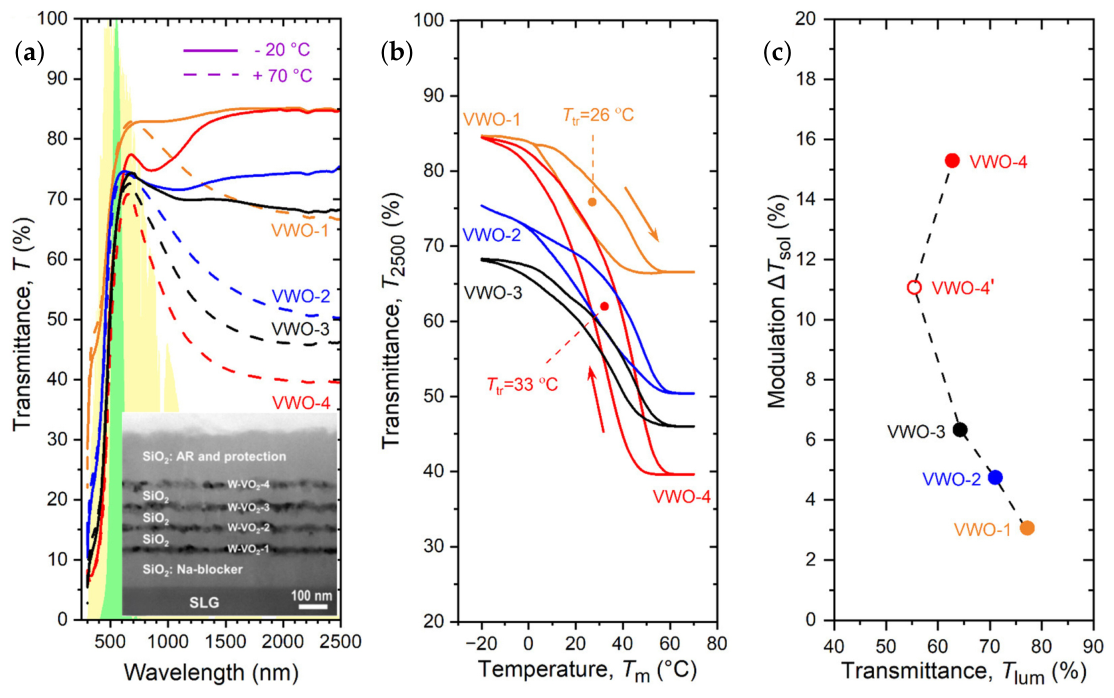
A further important contribution in this direction was reported by Vlček et al. [166], who demonstrated that the thermochromic performance of VO2-based coatings can be significantly improved by replacing the compact active layer with W-doped VO2 nanoparticles embedded in a SiO2 matrix. W was again selected to reduce the T c , while the nanoparticle morphology was selected to reduce the effective visible-range refractive index and extinction coefficient. The SiO2 matrix and overlayer were chosen because SiO2 has a low refractive index, n 1.46 at λ = 550 nm, negligible absorption with k < 10 3 at λ = 550 nm, and can simultaneously act as a Na-diffusion barrier, low-index matrix, AR medium, and protective layer. In addition, the metallic VO2(R) nanoparticles can enhance NIR absorption through localized surface plasmon resonance, which increases Δ T sol without excessively suppressing visible transmittance.
The coating reported by Vlček et al. was prepared on 1 mm SLG at a maximum substrate temperature of 350 ° C. The structure consisted of a bottom ∼100 nm SiO2 layer blocking Na diffusion from the glass substrate, four W-doped VO2 nanoparticle layers separated by three ∼50 nm SiO2 layers, and a top ∼160 nm SiO2 AR/protective overlayer. Each nanoparticle layer was obtained by depositing a ∼10 nm V–W film, annealing it up to 350 ° C for 1 h in pure oxygen at p O 2 = 15 Pa, cooling below 50 ° C, and depositing the next SiO2 layer. The V–W films were deposited from a V–W target containing 4.0 w t . % W, corresponding to 1.14 a t . % W, and the W-induced T c gradient was at least 24 ° C/at.% W.
TEM and HRTEM showed W-doped VO2 nanoparticles embedded in the SiO2 matrix, with representative vertical nanoparticle sizes of about 42 nm in the upper W–VO2 layer and about 22 nm in the lower W–VO2 layer (Figure 18a inset). SEM analysis showed that most nanoparticles had diameters of 41–55 nm and interparticle spacings of 7–21 nm, while some elongated particles reached lengths of 150–400 nm or even about 1 μ m.
The gradual increase in the number of W-doped VO2 layers produced the expected trade-off between visible transmittance and solar modulation. For one, two, three, and four nanoparticle layers with approximately 50 nm SiO2 overlayers, Δ T sol increased from 3.1 % to 4.7 % , 6.3 % , and 11.1 % , respectively, while the low-temperature T lum decreased from 76.3 % to 71.9 % , 64.9 % , and 56.8 % . Replacing the ∼50 nm top SiO2 overlayer in the four-layer coating with an optimized ∼160 nm top SiO2 AR/protective layer strongly improved the performance. The final VWO-4 coating reached T lum = 65.4 % at low temperature, T lum = 60.1 % at high temperature, T sol = 66.1 % at low temperature, T sol = 50.8 % at high temperature, Δ T lum = 5.3 % , Δ T sol = 15.3 % , and T c = 33 ° C [166]. This is the highest Δ T sol among the three selected approaches while still maintaining T lum > 60 % in both thermochromic states (Figure 18).
Overall, these studies illustrate a clear progression in VO2-based SW design. Becker et al. [164] demonstrated that buffer and AR layers can improve the optical performance of undoped VO2, but the resulting T lum remains limited by the intrinsic absorption of the active layer and by interface roughness. Kaufman et al. solved this limitation more effectively by combining W/Sr codoping with second-order YSZ/SiO2 AR design, reaching T c = 22 ° C, T lum > 60 % , and Δ T sol > 10 % in a compact multilayer coating prepared at 320 ° C [165]. Vlček et al. achieved the highest solar modulation by introducing W-doped VO2 nanoparticles into a SiO2 matrix, where the combination of reduced effective optical constants, localized near-infrared absorption, and optimized SiO2 AR/protection produced Δ T sol = 15.3 % while preserving T lum > 60 % [166]. Thus, the most promising direction is the simultaneous optimization of dopant chemistry, optical interference, layer morphology, and interface stability rather than the use of a single modification strategy.
In comparison with VO2 and other inorganic thermochromic material systems, PNIPAm-based hydrogels generally show superior optical performance. PNIPAm-AEMA hydrogel microparticles have shown T lum = 87.2 % , Δ T sol = 81.3 % , and a lower critical solution temperature (LCST) of around 32 ° C [173]. HBPEC/PNIPAm hydrogels reached T lum = 87.5 % , Δ T sol = 71.2 % , and a tunable transition range of 24.1 33.2 ° C [174]. PNIPAm/HEMC hydrogels were also reported with T lum 85 % and Δ T sol 75 % [149]. These values are substantially higher than those of most VO2 coatings, for which Δ T sol typically remains below 20 % . However, hydrogel systems face different device-integration challenges, including encapsulation, water retention, drying/freezing resistance, mechanical stability during swelling/deswelling, and long-term outdoor durability.
Emerging thermochromic systems occupy an intermediate position between VO2 and hydrogel-based systems. Metal-halide perovskite SWs based on CH3NH3PbI3 can exhibit visible transmittance above 85 % in the cold state and about 34.3 % in the hot state, with Δ T sol = 25.5 % and a transition temperature of approximately 54.4 ° C [175]. Hydrated ionic polymers, such as [ ( C 2 H 5 ) 2 NH 2 ] 2 NiCl 4 @PVP-type systems, combine T lum = 87.7 % , Δ T sol = 30.5 % , and a tunable transition temperature of 25– 42 ° C [176]. Commercial IR-selective thermochromic coatings, such as SunSmart coatings, show more moderate but application-oriented values, with T lum 70 75 % and Δ T sol 20 23 % [177]. Cholesteric liquid-crystal thermochromic films are promising for selective NIR modulation and composition-tunable optical response, although their performance metrics are less standardized than those of VO2 or PNIPAm-based systems [178].
These comparisons indicate that the most effective SW designs will likely rely on combining the strengths of different material classes rather than selecting a single universal material system. VO2 offers inorganic stability, compatibility with thin film processing, and strong NIR switching, but it still requires simultaneous improvement of T c , T lum , Δ T sol , color neutrality, interface quality, and scalable deposition. Hydrogels provide the highest optical performance, with T lum > 85 % and Δ T sol > 70 % , but their long-term durability and encapsulation remain unresolved. Perovskites and hydrated ionic polymers offer high contrast and tunable transition temperatures, but they require further validation with respect to toxicity, humidity resistance, UV stability, hysteresis, and cycling lifetime. Commercial IR-selective coatings are closer to real glazing implementation, but their optical modulation is lower than that of laboratory hydrogel systems.

4.2. Electrochromic WO3- and NiO-Based Smart Windows

Among electrochromic materials for SW applications, TMOs remain the most extensively investigated class because they combine reversible optical modulation, chemical robustness, thermal stability, and compatibility with conventional thin film fabrication methods. In TMO-based electrochromic SWs, the optical response is governed by electrically driven redox reactions coupled with the insertion/extraction of ions, such as H + , Li + , Na + . Therefore, the electrochromic performance is determined not only by the intrinsic optical contrast of the active oxide, but also by ion-diffusion kinetics, CT reversibility, electrolyte compatibility, and long-term cycling stability.
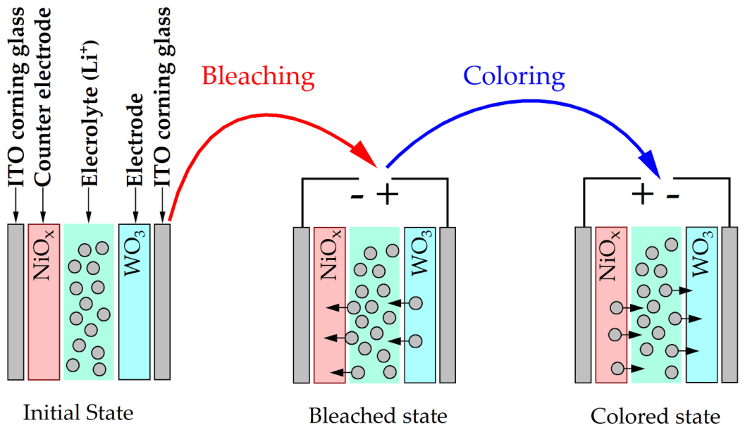
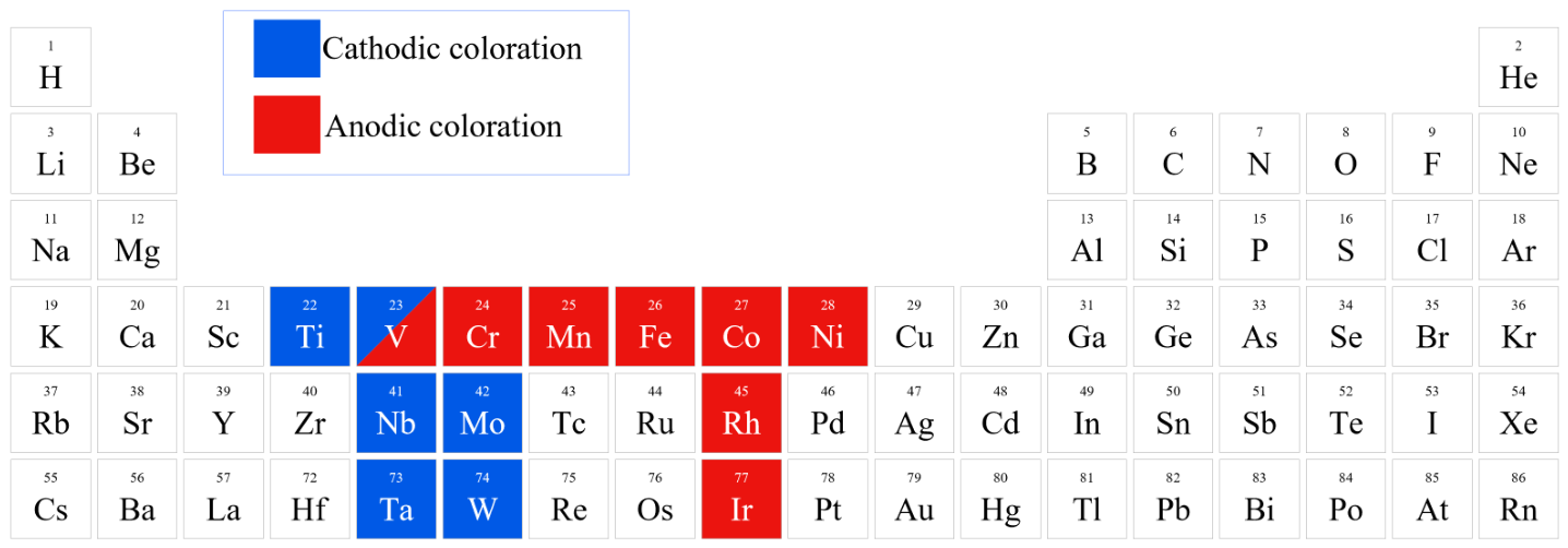
WO3 serves as the benchmark cathodic electrochromic oxide. Upon application of a suitable voltage, electrons are injected into the WO3 layer while charge-compensating ions from the electrolyte are inserted into its structure, forming a colored tungsten-bronze-like state, generally described as M x WO3, where M represents the inserted ion. When the voltage polarity is reversed, ions and electrons are extracted and the material returns to its bleached transparent state. In contrast, NiO is the prototypical anodic oxide counterpart, where coloration is associated with oxidation of Ni2+ toward higher-valence nickel states, such as Ni3+ and Ni4+. Consequently, the complementary integration of cathodic WO3 and anodic NiO remains one of the standard configurations for high-contrast electrochromic SWs.
Besides the benchmark WO3/NiO pair, other TMOs can also contribute to electrochromic functionality. V2O5 is attractive because its layered framework enables ion intercalation, multicolor switching, and infrared modulation, although structural stabilization is often required to improve cycling durability. TiO2, especially in anatase or nanostructured form, is frequently employed either as a weak active electrochromic component or, more importantly, as an ion-storage, passivation, or interfacial layer in all-inorganic and multilayer electrochromic architectures. TMOs are commonly classified into cathodically coloring and anodically coloring materials, depending on the polarity and redox process responsible for coloration [179] (Figure 19).
A typical electrochromic SW consists of two transparent substrates coated with transparent conducting layers, between which an electrochromic layer, an ion-conducting electrolyte, and a complementary counter-electrode or ion-storage layer are arranged in a sandwich-type architecture. Under an applied voltage, ions migrate through the electrolyte toward one electrode, while electrons are supplied through the external circuit. In the colored state, ion/electron insertion into the cathodic layer, most commonly WO3, increases optical absorption in the VIS and/or NIR region. At the same time, the anodic counter electrode, typically NiO or a Ni-containing oxide, balances the charge and can provide complementary coloration. Reversing the voltage extracts the inserted ions and electrons, restoring the bleached state. Therefore, the optical modulation of an electrochromic SW is a device-level response controlled by the active oxide layers, the transparent conductors, the electrolyte, and the stability of their interfaces (Figure 20).
The electrolyte controls ionic conductivity, switching speed, charge compensation, optical memory, leakage resistance, and interfacial degradation. Liquid and gel electrolytes generally provide high ionic conductivity and faster switching, but may suffer from leakage, evaporation, gas formation, and sealing problems. In contrast, solid polymer, inorganic, and hybrid electrolytes are more attractive for all-solid-state laminated windows because they improve mechanical integrity and device stability, although their ionic conductivity can be lower. Typical electrolyte types used in TMO-based electrochromic windows are summarized in Table 18.
TMOs practical relevance cannot be assessed only from the maximum optical contrast. Recent WO3 nanosheet/ITO nanocomposites reached optical modulation values up to Δ T 88 % and a coloration efficiency (CE) of 154.16 cm 2 C 1 [184]. Rare-earth-modified WO3 also shows strong performance: Tb-doped amorphous WO3 exhibited an optical contrast of 78.34 % , a CE of 138.82 cm 2 C 1 , and coloration/bleaching times of 16.0 / 11.4 s [185]. These values are high enough to justify the continued dominance of WO3 in electrochromic SW research, especially when compared with many other oxide systems. Nevertheless, WO3 suffers from the classical limitations of cathodic oxide electrochromics: repeated H+ or Li+ insertion/extraction can produce ion trapping, defect accumulation, local structural disorder, incomplete bleaching, and gradual loss of optical reversibility. Therefore, a WO3 film showing Δ T > 70 % in the first cycles is not necessarily suitable for practical glazing unless the same modulation is retained over thousands of cycles.
Recent improvements in WO3-based devices clearly show that interface engineering is more effective than simple single-layer optimization. For example, WO3/TiO2 electrochromic devices achieved Δ T = 73.9 % at 600 nm , CE up to 69 cm 2 C 1 , coloration times of about 20– 21 s , and stable operation over more than 1000 cycles [186]. More advanced TiO2/WO3/TiO2 double-heterojunction structures achieved a much higher CE of 479.3 cm 2 C 1 and retained 94.72 % of their transmission modulation after 7000 cycles under recovery conditions [187]. This comparison is important because the CE of the TiO2/WO3/TiO2 heterostructure is more than three times higher than that of the WO3 nanosheet/ITO nanocomposite and more than six times higher than the WO3/TiO2 device. Although TiO2 alone is usually a weak visible electrochromic material, in multilayer devices it acts as an ion-storage, passivation, or interfacial layer that suppresses irreversible ion accumulation and improves CT reversibility.
NiO is the most important anodic oxide counterpart to WO3 in complementary electrochromic devices. Recent W6+-doped NiO films showed an optical modulation of 61.56 % at 550 nm , a CE of 45.41 cm 2 C 1 , fast switching times of 4.42 / 1.40 s for coloration/bleaching, and stable operation over 2000 cycles [188]. These figures indicate that NiO can switch faster than many WO3 systems, but its CE remains lower than that of optimized WO3, Prussian Blue, PANI, or PEDOT:PSS. Thus, NiO is not generally selected because it provides the highest CE, but because it is one of the most suitable anodic charge-balancing layers for WO3-based full devices. Its main limitations are its relatively low electrical conductivity, moderate CT kinetics, and degradation during prolonged cycling, which explains why doping, defect engineering, and nanostructuring are required for practical SW integration.
Alternative Ni-based compounds can provide stronger optical modulation than conventional NiO. Electrodeposited NiHPO 4 · 3H2O films demonstrated an optical modulation of 90.8 % at 500 nm and a CE of 75.4 cm 2 C 1 , while also enabling a large-area electrochromic device with an active area of 100 cm 2 [189]. The Δ T value of 90.8 % is higher than that reported for the WO3 nanosheet/ITO system, Tb-doped WO3, W-doped NiO, V2O5, PANI, PEDOT:PSS, and viologen/PEDOT:PSS/Zn devices considered here. From a manufacturing perspective, electrodeposition is also attractive because it is lower-cost and more scalable than pulsed laser deposition or high-vacuum multilayer deposition. However, the long-term outdoor durability of nickel phosphate under humidity, UV exposure, thermal cycling, and realistic electrolyte conditions still requires further validation.
TiO2 should be considered separately from WO3 and NiO because its role in SWs is often interfacial rather than purely electrochromic. TiO2-based heterostructures, such as 2D TiO2/Ti3 C 2 T x MXene systems, have been reported to provide high optical modulation, fast response, and good mechanical stability in flexible devices [190]. In Au nanoparticle-loaded TiO2 nanofibrous layers, the optical modulation was approximately Δ T 40 % , the CE was about 20 cm 2 C 1 , the switching time was around 6 s , and the devices operated for more than 1000 cycles [191]. These values are lower than those of optimized WO3 or conducting-polymer systems, but TiO2 remains highly valuable because it can improve cycling stability, protect active layers, assist ion storage, and enable flexible or nanostructured device architectures.
V2O5 is attractive because it offers multicolor electrochromism and very fast switching. Annealed V2O5 films showed a bleached transmittance of T b = 71.89 % , a colored transmittance of T col = 29.57 % , an optical modulation of Δ T = 42.32 % , a CE of 34.93 cm 2 C 1 , and very short coloration/bleaching times of 0.4 / 3.0 s [192]. The switching speed of V2O5 is therefore better than that of many WO3-based devices and comparable to fast polymer systems. However, its optical contrast can degrade significantly after only about 100 cycles, which is far below the 2000 cycles reported for W-doped NiO, the 7000 cycles reported for TiO2/WO3/TiO2, and the 10,000 cycles reported for PANI-based devices. This makes V2O5 promising for rapid or multicolor electrochromic functions, but still problematic for long-lifetime architectural glazing.
When TMOs are compared with non-oxide electrochromic materials, the differences become even clearer. Nanogranular Prussian Blue films reached optical modulation values of about 80 % , CEs as high as 417.79 cm 2 C 1 , and 91.4 % optical contrast retention [193]. Thus, the CE of Prussian Blue is approximately 2.7 times higher than that of the WO3 nanosheet/ITO system, about 9.2 times higher than that of W-doped NiO, and about 12 times higher than that of V2O5. This demonstrates the strong charge-utilization advantage of Prussian Blue, although its dominant blue coloration and electrolyte sensitivity can limit its use in color-neutral architectural glazing.
Conducting polymers also show highly competitive electrochromic performance. Polyaniline-based dual-band electrochromic SWs demonstrated Δ T = 65 % at 633 nm and Δ T = 59 % at 1600 nm , with CEs of 367.1 cm 2 C 1 in the visible region and 299.6 cm 2 C 1 in the NIR region, together with stability exceeding 10,000 cycles [194]. This is particularly important because dual-band modulation allows independent control of visible light and solar heat, a functionality that most single-component oxide systems cannot easily provide. PEDOT:PSS-based devices achieved an optical contrast of 47.9 % at 635 nm , a CE of 352 cm 2 C 1 , and very fast switching times of 1.6 / 0.6 s [195]. Although the optical contrast of PEDOT:PSS is lower than that of WO3, Prussian Blue, or PANI, its switching speed and solution processability make it attractive for printed, flexible, and low-temperature electrochromic devices.
Viologen-based hybrid systems further illustrate the advantages of organic electrochromics. Viologen/PEDOT:PSS/Zn devices reached an optical difference of 64.23 % , a CE of 389.44 cm 2 C 1 , switching times of 1.6 / 0.8 s , and 90.58 % retention of Δ T [196]. The CE of this hybrid system is higher than that of WO3, NiO, nickel phosphate, TiO2, and V2O5, and its switching is faster than most oxide systems. However, aqueous organic–metal hybrid devices may suffer from swelling, electrolyte leakage, dissolution, interfacial instability, and degradation of organic redox species during prolonged outdoor exposure. Therefore, their excellent short-term electrochemical performance must be balanced against environmental durability requirements.
A direct performance comparison therefore shows that each material class has a distinct advantage. WO3 provides high optical modulation, with values up to Δ T 88 % , and remains the most reliable cathodic oxide. NiO provides fast anodic switching, with 4.42 / 1.40 s switching times and 2000-cycle stability, but lower CE. TiO2 improves interfaces and cycling stability rather than acting as the strongest active electrochromic layer. V2O5 provides very fast switching, down to 0.4 s for coloration, but poor cycling stability. Nickel phosphate provides very high optical modulation of 90.8 % and scalable electrodeposition. Prussian Blue, PANI, PEDOT:PSS, and viologen systems provide much higher CE values, typically in the range of 352– 417.79 cm 2 C 1 , but their environmental stability is generally more problematic than that of inorganic oxides.
From the viewpoint of deposition and manufacturing, TMOs are compatible with magnetron sputtering, PLD, ALD, sol–gel processing, and electrodeposition. Vacuum-based methods such as sputtering and ALD offer dense, uniform, and reproducible coatings, which are essential for large-area optical uniformity, but they increase equipment cost and may limit low-cost manufacturing. PLD is useful for high-quality research films but is less attractive for industrial-scale glazing. Sol–gel processing and electrodeposition are more scalable and cost-effective, as illustrated by the 100 cm 2 nickel phosphate device, but they require strict control of film porosity, adhesion, crystallinity, and post-treatment. Processing temperature is also critical: high-temperature annealing can improve oxide crystallinity and cycling stability, whereas low-temperature processing is required for flexible substrates, polymers, and laminated window structures.
At the device level, electrolyte compatibility is as important as the active electrochromic material. H+, Li+, Na+, Zn2+, and other mobile ions can provide electrochromic switching, but they also determine diffusion kinetics, reversibility, charge compensation, interfacial stability, and degradation pathways. Dense WO3 films may suffer from slow ion diffusion and ion trapping, whereas organic and hydrogel-like devices may suffer from swelling, leakage, or dissolution. A device with high CE is therefore not automatically superior if the electrolyte causes gas evolution, parasitic redox reactions, delamination, or rapid loss of optical memory. For practical SWs, the target is not simply the highest Δ T or CE, but the best combination of optical contrast, response speed, cycling lifetime, color neutrality, haze control, sealing, and compatibility with large-area laminated glazing.
These comparison shows that no single electrochromic material currently maximizes all relevant parameters. WO3 remains the benchmark cathodic oxide because it provides high optical modulation and relatively strong durability. NiO remains the preferred anodic oxide because it enables complementary WO3-based devices. TiO2 is most valuable as an interfacial and stabilizing component. V2O5 is attractive for rapid and multicolor switching but is limited by cycling degradation.
For commercial applications, ITO, FTO, AZO, and PEDOT or PEDOT-based transparent conducting coatings are widely used.
At present, a relatively large number of both major and smaller companies are involved in the production of electrochromic SW. Table 19 summarizes selected commercial products from four companies chosen for this review, as they represent different technological, commercial, and manufacturing approaches within the SW sector. A common feature of these products is the use of a WO3/NiO cathode–anode configuration.
However, the exact layer chemistry used in commercial electrochromic SWs is rarely disclosed in current product literature and is generally treated as proprietary. Publicly available information is therefore often fragmentary and must be reconstructed from patents, older technical brochures, and review papers. Taken together, these sources suggest that many commercially relevant inorganic electrochromic SW platforms rely on a tungsten-oxide-based cathodic layer combined with a nickel-oxide-based, nickel-containing, or mixed tungsten–nickel anodic/counter electrode, frequently in lithiated or otherwise compositionally modified form rather than as strictly stoichiometric WO3 and NiO. Accordingly, the systems listed in Table 19 are best described as devices that, with a high degree of confidence, appear to belong to the broader WO3/NiO materials family.

4.3. Optical Hydrogen Detection Using TMO-Based Gasochromic Sensors

Hydrogen leakage detection is a critical safety requirement because H 2 [197]: (i) is flammable over a wide concentration range in air, typically ∼4– 75 vol . % ; (ii) exhibits an extremely low minimum ignition energy, 0.017 mJ ; (iii) is colorless, odorless, and tasteless, making leaks difficult to notice without instrumentation; (iv) can cause hydrogen embrittlement of structural materials, thereby increasing the probability of failures and leakage.
Gasochromic hydrogen sensors [197] provide an optical route to leak detection by converting the gas–solid interaction into a reversible change of the materials’ optical response, such as transmittance, reflectance, absorbance, or perceived color. In TMO materials, the gasochromic response is commonly attributed to near-surface redox reactions, intercalation–deintercalation, which result in increased absorption in the VIS–NIR region. Gasochromic hydrogen sensors have several key features: (i) they can operate at room temperature and may not require external electrical biasing at the sensing element, reducing ignition risks; (ii) hydrogen exposure can induce a distinct optical contrast, including visible color changes in some systems, enabling direct visual indication and straightforward optical readout; (iii) the device concept can be implemented using simple thin film stacks and low-cost optical interrogation, e.g., photodiodes or cameras, which is attractive for scalable safety indicators.
Among TMOs, tungsten trioxide WO3 is widely applicable as one of the most practically established materials for optical hydrogen detection [197]. This preference is largely driven by its pronounced and reversible optical modulation upon hydrogen exposure, typically a pale-yellow to deep-blue coloration [198,199]. In most device implementations, WO3 is combined with a thin Pd or Pt catalytic overlayer to dissociate H2 and promote spillover/insertion, enabling large changes in transmittance with good repeatability [200]. These features make Pd/Pt–WO3 coatings a common choice for passive, optically readable hydrogen-leak indicators [199,201].
Vanadium oxides represent another important gasochromic TMO class for hydrogen optical sensing [197]. In particular, V2O5 thin films, often combined with a noble-metal catalyst such as Pt, exhibit a pronounced and reversible optical contrast upon H2 exposure under ambient conditions, e.g., from yellow to gray/black, consistent with hydrogen-driven redox processes [202,203,204]. In parallel, VO2 is frequently exploited in a distinct route, where the gas environment, hydrogenation, shifts the MIT and produces a large change in resistance [205,206]. The MIT in VO2 is accompanied by a strong modulation of optical constants, especially in the NIR/MIR region, so a gas-induced MIT shift can, in principle, be read out optically as well, either as a gasochromic contrast or as an MIT-assisted transmittance/reflectance change [207].
In contrast to WO3 and several vanadium oxides, NiO [208] and TiO2 [209] are most commonly deployed as chemiresistive metal oxide (MOX) sensors, where the primary signal is a gas-induced change in conductivity rather than a pronounced, reversible optical contrast. Nevertheless, both oxides can still be integrated into optically readable sensor architectures at the device level. For NiO, its well-known anodic electrochromism under ion intercalation–deintercalation can be leveraged as a visual transducer in electrochromic sensor concepts, where a gas-driven electrochemical/potentiometric process is converted into a measurable optical modulation of the NiO layer [8,210]. For TiO2, a practical route toward optical/low-temperature operation is photoactivated sensing, where UV illumination modifies surface charge chemistry and enables room-temperature or reduced-temperature gas detection, with optical control and straightforward optical interrogation schemes [209,211]. Finally, TiO2 can develop Ti3+ or oxygen-vacancy centers under strongly reducing, hydrogenating treatments, producing blue/black optical states. This suggests a possible gas-induced optical pathway, although this typically requires elevated temperatures and careful engineering to ensure reversibility and selectivity [212,213].

5. Future Perspectives

The development of chromic TMO thin films is moving from the optimization of individual films toward the design of complete device architectures. The central issue is the simultaneous control of optical, ionic, electronic, mechanical, and environmental parameters within the same structure.
For thermochromic VO2, the relevant performance window combines T c close to 20– 35 ° C , T lum > 60 % , Δ T sol > 10 15 % , narrow hysteresis, and stable optical response during repeated heating and cooling. For electrochromic devices, the technologically meaningful range combines Δ T > 60 80 % , C E > 100 cm 2 C 1 where attainable, coloration/bleaching below 10– 20 s at device scale, and optical-modulation retention above 90 % after 5000–10,000 cycles. These combined targets are more restrictive than isolated record values and therefore represent a more realistic criterion for SW integration.
VO2 demonstrates the balance between material improvement and optical trade-off. W/Sr-codoped VO2 multilayers can reduce T c to 22 ° C while maintaining T lum = 63.7 % in the low-temperature state and 60.7 % in the high-temperature state, with T sol decreasing from 58.8 % to 47.6 % and Δ T sol = 11.2 % [165]. W-doped VO2/SiO2 nanoparticle coatings reach T lum = 65.4 % and 60.1 % in the low- and high-temperature states, Δ T sol = 15.3 % , and T c = 33 ° C [166].
AI and machine-learning approaches provide a route for treating chromic oxides as multi-parameter systems. In NiO, recent machine-learning studies mainly concern optical-property prediction in RF-magnetron-sputtered or doped films [214,215]. Machine learning has been used to connect WO3 sputtering parameters with electrochromic reversibility and blue-color persistence [216]. In an ammonium metatungstate/FeCl2/D2O a multilayer perceptron model trained on 25 devices enabled a device with Δ T = 74 % , coloration and bleaching times of 6.5 and 13.5 s , and stability above 1000 cycles [217]. Another machine-learning-guided all-liquid electrochromic device reached Δ T = 62.6 % with response times of 5.7 and 7.1 s [218]. Long short-term memory (LSTM) modelling has also been applied to cycle-life prediction, giving Δ T = 43.95 % , coloration/bleaching times of 7 and 8 s , and Δ T = 44.92 % after 1000 cycles [219]. Overall, AI is useful for device and multilayer structure optimization, and also for property prediction.
Interface engineering represents a decisive factor in both thermochromic and electrochromic oxide devices. In VO2 multilayers, a few nanometers of interfacial roughness can change the optical response substantially. For TiO2/VO2/TiO2 stacks, an ideal model predicted T lum of about 45 % , whereas the introduction of effective-medium interface layers of only 4– 5 nm and 8– 10 nm reduced the calculated T lum to approximately 35– 37 % [164]. Thus, nominal layer thickness is not sufficient for describing real optical stacks. Interface roughness, interdiffusion width, oxidation-state gradients, and the optical constants of the actual multilayer determine the final coating performance [6,164]. In electrochromic devices, WO3/electrolyte, NiO/electrolyte, TiO2/WO3, and transparent-conductor/oxide interfaces control CT resistance, ion trapping, incomplete bleaching, and long-term drift [186,220,221]. The high CE reported for TiO2/WO3/TiO2 heterostructures shows that TiO2 can operate as an active interfacial component that improves CT reversibility and suppresses irreversible ion accumulation [186,187].
Nanostructuring is effective only when optical gain, ion transport, and durability remain balanced. In W-doped VO2/SiO2 nanoparticle coatings, increasing the number of nanoparticle layers from one to four increased Δ T sol from 3.1 % to 11.1 % , but decreased low-temperature T lum from 76.3 % to 56.8 % [166]. After optimization of the SiO2 AR/protective layer, the coating reached T lum = 65.4 % , Δ T sol = 15.3 % , and T c = 33 ° C [166]. In electrochromic WO3, NiO, and V2O5, nanosheets, porous films, nanofibers, and nanocomposites reduce ion-diffusion length and increase electrochemically active surface area [182,184,222,223,224]. At the same time, excessive porosity and uncontrolled open morphology can increase electrolyte penetration, local structural distortion, irreversible ion trapping, incomplete ion extraction, and cycling degradation [11,192,222]. V2O5 demonstrates this trade-off clearly: coloration and bleaching times of 0.4 and 3.0 s are very fast, but degradation after about 100 cycles remains incompatible with long-life smart-window operation [192].
Flexible and large-area devices introduce constraints that are not visible in small-area cells. Commercial electrochromic glazing already reaches dimensions of several square meters (Table 19) In contrast, many laboratory TMO devices are tested on areas of only a few cm 2 . Scaling from cm 2 to m 2 changes the dominant limitations: sheet resistance, lateral voltage drop, electrolyte distribution, edge sealing, defect density, and non-uniform coloration become central performance factors [180,225]. Flexible devices add another set of variables, including bending radius, number of bending cycles, Δ T retention after bending, adhesion loss, electrolyte leakage, and change in sheet resistance [226,227]. Optical modulation measured before bending is therefore insufficient for evaluating flexible electrochromic devices, because mechanical stability, electrochemical reversibility, electrode conductivity, and encapsulation integrity must also be retained after repeated deformation [182,190].
Overall, AI-assisted optimization, flexible processing, interface engineering, and nanostructuring are connected strategies for achieving reproducible device performance under realistic optical, electrochemical, mechanical, and environmental conditions.

6. Conclusions

Chromic TMO thin films are promising materials for adaptive optical technologies, including SWs, optical switching, gas sensing, and multifunctional coatings. The systems discussed in this review, namely VO2 and related vanadium oxides, WO3, NiO, and TiO2, show that chromic behavior is controlled by the interplay between crystal structure, electronic configuration, oxidation state, oxygen stoichiometry, defects, ion transport, and thin film microstructure. Thus, their optical response must be understood not only from chemical composition, but also from phase purity, morphology, interfaces, and preparation conditions.
VO2 remains the reference thermochromic oxide because its MIT transition enables passive temperature-driven optical modulation, especially in the NIR region. WO3 and NiO are key electrochromic oxides, with performance governed by ion insertion/extraction, charge compensation, crystallinity, porosity, electrolyte compatibility, and cycling stability. V2O5 extends chromic functionality toward multicolor electrochromism and gas sensing, whereas TiO2 is important as a defect-active oxide and as an auxiliary layer in electrochromic, photocatalytic, antireflective, and optoelectronic architectures.
The preparation route is a decisive factor for chromic performance. Deposition and post-treatment conditions control thickness, stoichiometry, crystallinity, morphology, defects, and interfaces, which directly affect optical contrast, switching kinetics, stability, and reproducibility. Therefore, efficient chromic coatings require the simultaneous optimization of material composition, thin film processing, and device architecture.
Despite significant progress, several challenges remain. VO2-based systems still require better control of transition temperature, hysteresis, visible transparency, solar modulation, and long-term stability. WO3-, NiO-, V2O5-, and TiO2-based systems are often limited by ion-transport constraints, charge trapping, slow switching, structural fatigue, and cycling degradation. These limitations are especially important for SW applications, where high luminous transmittance, strong solar modulation, color neutrality, durability, and large-area manufacturability must be achieved simultaneously.
Future research should focus on the following directions:
improving VO2 thermochromic coatings through reducing the transition temperature while preserving high luminous transmittance, strong solar modulation, narrow hysteresis, and environmental stability through doping, strain engineering, multilayer design, protective layers, and nanostructuring;
enhancing WO3/NiO-based electrochromic oxide devices, namely faster switching, lower operating voltage, higher optical contrast, better color neutrality, and longer cycling lifetime through improved ion transport, electrolyte compatibility, charge balance, and interface stability;
controlling defects and microstructure such as oxygen vacancies, mixed-valence states, grain boundaries, and porosity to tune optical modulation, ion diffusion, switching kinetics, and degradation;
expanding gasochromic WO3 and V2O5 devices for hydrogen sensing and optical gas detection through improving sensitivity, selectivity, reversibility, humidity tolerance, and stable low-temperature operation.
Overall, future TMO films should be compatible with scalable deposition methods, large-area and flexible substrates, and multilayer architectures, while combining chromism with antireflection, photocatalysis, sensing, thermal regulation, or energy-related functions.

Author Contributions

Conceptualization, Ş.-A.I., J.L. and S.V.; software, G.G. and A.V.; validation, G.G., A.V., Ş.-A.I., J.L. and S.V.; investigation, G.G. and A.V.; resources, Ş.-A.I., J.L. and S.V.; data curation, G.G., A.V., Ş.-A.I., J.L. and S.V.; writing–original draft preparation, G.G. and A.V.; writing–review and editing, G.G., A.V., Ş.-A.I., J.L. and S.V.; visualization, G.G. and A.V.; supervision, Ş.-A.I., J.L. and S.V.; project administration, Ş.-A.I., J.L. and S.V.; funding acquisition, Ş.-A.I., J.L. and S.V. All authors contributed equally to this work. All authors have read and agreed to the published version of the manuscript.

Funding

This work was supported by CNCS-UEFISCDI through the Bilateral Romania-Moldova project DUALCHROM, Grant No. 18ROMD/20.05.2024, PN-IV-P8-8.3-ROMD-2023-0186; and by the Ministry of Education and Research of the Republic of Moldova through the research subproject Abundant-element-based materials and structures for radiation detection and efficient energy conversion, Grant No. 011207 DETCONV.

Data Availability Statement

No new data were created or analyzed in this study. Data sharing is not applicable to this article.

Conflicts of Interest

The authors declare no conflicts of interest.

Abbreviations

The following abbreviations are used in this manuscript:
AACVDAerosol-assisted chemical vapor deposition
AFIAntiferromagnetic insulating
ALDAtomic layer deposition
ARAntireflection
AZOAluminum-doped zinc oxide
CEColoration efficiency
CTCharge-transfer
CVDChemical vapor deposition
DFTDensity functional theory
DGUDouble glazing unit
ECWElectrochromic window
HiPIMSHigh-power impulse magnetron sputtering
HRTEMHigh-resolution transmission electron microscopy
IGUInsulating glass unit
IRInfrared
ITOIndium tin oxide
LCSTLower critical solution temperature
LPCVDLow-pressure chemical vapor deposition
LPEsLiquid/liquid-polymer electrolytes
MBEMolecular beam epitaxy
MIRMid-infrared
MITMetal–insulator transition
MOXMetal oxide
NIRNear-infrared
PCPropylene carbonate
PLDPulsed laser deposition
RFMSRadio-frequency magnetron sputtering
RHRelative humidity
SEMScanning electron microscopy
SHGCSolar heat gain coefficient
SLGSoda-lime glass
SPEsSolid polymer electrolytes
SWSmart window
SWsSmart windows
TEMTransmission electron microscopy
TGUTriple glazing unit
TMMTransfer matrix method
TMOTransition metal oxide
TMOsTransition metal oxides
UVUltraviolet
VISVisible
YSZYttria-stabilized zirconia

References

  1. Yan, D.; Wang, Z.; Zhang, Z. Stimuli-Responsive Crystalline Smart Materials: From Rational Design and Fabrication to Applications. Acc. Chem. Res. 2022, 55, 1047–1058. [Google Scholar] [CrossRef] [PubMed]
  2. Stuart, M.A.C.; Huck, W.T.S.; Genzer, J.; Müller, M.; Ober, C.; Stamm, M.; Sukhorukov, G.B.; Szleifer, I.; Tsukruk, V.V.; Urban, M.; et al. Emerging Applications of Stimuli-Responsive Polymer Materials. Nat. Mater. 2010, 9, 101–113. [Google Scholar] [CrossRef] [PubMed]
  3. Imato, K.; Ooyama, Y. Stimuli-Responsive Smart Polymers Based on Functional Dyes. Polym. J. 2024, 56, 1093–1109. [Google Scholar] [CrossRef]
  4. Wu, S.; Sun, H.; Duan, M.; Mao, H.; Wu, Y.; Zhao, H.; Lin, B. Applications of Thermochromic and Electrochromic Smart Windows: Materials to Buildings. Cell Rep. Phys. Sci. 2023, 4, 101370. [Google Scholar] [CrossRef]
  5. Cannavale, A.; Ayr, U.; Fiorito, F.; Martellotta, F. Smart Electrochromic Windows to Enhance Building Energy Efficiency and Visual Comfort. Energies 2020, 13, 1449. [Google Scholar] [CrossRef]
  6. Jiang, C.; He, L.; Xuan, Q.; Liao, Y.; Dai, J.G.; Lei, D. Phase-Change VO2-based Thermochromic Smart Windows. Light Sci. Appl. 2024, 13, 255. [Google Scholar] [CrossRef] [PubMed]
  7. Shchegolkov, A.V.; Jang, S.H.; Shchegolkov, A.V.; Rodionov, Y.V.; Sukhova, A.O.; Lipkin, M.S. A Brief Overview of Electrochromic Materials and Related Devices: A Nanostructured Materials Perspective. Nanomaterials 2021, 11, 2376. [Google Scholar] [CrossRef] [PubMed]
  8. Seok, H.; Son, S.; Cho, J.; Choi, S.; Park, K.; Kim, C.; Jeon, N.; Kim, T.; Kim, H.U. Chromism-Integrated Sensors and Devices for Visual Indicators. Sensors 2022, 22, 4288. [Google Scholar] [CrossRef] [PubMed]
  9. Mustafa, M.N.; Mohd Abdah, M.A.A.; Numan, A.; Moreno-Rangel, A.; Radwan, A.; Khalid, M. Smart Window Technology and Its Potential for Net-Zero Buildings: A Review. Renew. Sustain. Energy Rev. 2023, 181, 113355. [Google Scholar] [CrossRef]
  10. Fu, H.; Zhang, L.; Dong, Y.; Zhang, C.; Li, W. Recent Advances in Electrochromic Materials and Devices for Camouflage Applications. Mater. Chem. Front. 2023, 7, 2337–2358. [Google Scholar] [CrossRef]
  11. Zhang, Y.; Ding, Y.; Lan, F.; Zhang, W.; Li, J.; Zhang, R. Recent Advances in Tungsten Oxide-Based Chromogenic Materials: Photochromism, Electrochromism, and Gasochromism. Nanoscale 2024, 16, 21279–21293. [Google Scholar] [CrossRef] [PubMed]
  12. Rao, C.N.R. Transition Metal Oxides. Annu. Rev. Phys. Chem. 1989, 40, 291–326. [Google Scholar] [CrossRef]
  13. Ahn, C.; Cavalleri, A.; Georges, A.; Ismail-Beigi, S.; Millis, A.J.; Triscone, J.M. Designing and Controlling the Properties of Transition Metal Oxide Quantum Materials. Nat. Mater. 2021, 20, 1462–1468. [Google Scholar] [CrossRef] [PubMed]
  14. Yu, X.; Marks, T.J.; Facchetti, A. Metal Oxides for Optoelectronic Applications. Nat. Mater. 2016, 15, 383–396. [Google Scholar] [CrossRef] [PubMed]
  15. Agnihotri, A.S.; Varghese, A.; M, N. Transition Metal Oxides in Electrochemical and Bio Sensing: A State-of-Art Review. Appl. Surf. Sci. Adv. 2021, 4, 100072. [Google Scholar] [CrossRef]
  16. Hidayat, R.; Aftab, S.; Khalid, A.; Hegazy, H.H.; Rajpar, A.H.; Rubab, N.; Yewale, M.A. Transition Metal Oxides for Battery Technologies. J. Alloy. Compd. 2025, 1039, 183257. [Google Scholar] [CrossRef]
  17. Ganduglia-Pirovano, M.V.; Hofmann, A.; Sauer, J. Oxygen Vacancies in Transition Metal and Rare Earth Oxides: Current State of Understanding and Remaining Challenges. Surf. Sci. Rep. 2007, 62, 219–270. [Google Scholar] [CrossRef]
  18. Nilius, N. Properties of Oxide Thin Films and Their Adsorption Behavior Studied by Scanning Tunneling Microscopy and Conductance Spectroscopy. Surf. Sci. Rep. 2009, 64, 595–659. [Google Scholar] [CrossRef]
  19. Cao, Z.; Li, S.; Xie, W.; Du, G.; Qiao, Z. Critical Evaluation and Thermodynamic Optimization of the V–O System. Calphad 2015, 51, 241–251. [Google Scholar] [CrossRef]
  20. Hu, P.; Hu, P.; Vu, T.D.; Li, M.; Wang, S.; Ke, Y.; Zeng, X.; Mai, L.; Long, Y. Vanadium Oxide: Phase Diagrams, Structures, Synthesis, and Applications. Chem. Rev. 2023, 123, 4353–4415. [Google Scholar] [CrossRef] [PubMed]
  21. Longo, J.M.; Kierkegaard, P.; Ballhausen, C.J.; Ragnarsson, U.; Rasmussen, S.E.; Sunde, E.; Sørensen, N.A. A Refinement of the Structure of VO2. Acta Chem. Scand. 1970, 24, 420–426. [Google Scholar] [CrossRef]
  22. Marezio, M.; McWhan, D.B.; Remeika, J.P.; Dernier, P.D. Structural Aspects of the Metal-Insulator Transitions in Cr-Doped V O 2. Phys. Rev. B 1972, 5, 2541–2551. [Google Scholar] [CrossRef]
  23. Park, J.H.; Coy, J.M.; Kasirga, T.S.; Huang, C.; Fei, Z.; Hunter, S.; Cobden, D.H. Measurement of a Solid-State Triple Point at the Metal–Insulator Transition in VO2. Nature 2013, 500, 431–434. [Google Scholar] [CrossRef] [PubMed]
  24. Eyert, V. The Metal-insulator Transitions of VO2: A Band Theoretical Approach. Ann. Phys. 2002, 514, 650–704. [Google Scholar] [CrossRef]
  25. Vincent, M.G.; Yvon, K.; Ashkenazi, J. Electron-density studies of metal–metal bonds. I. The deformation density of V2O3 at 295 K. Acta Crystallogr. Sect. A 1980, 36, 814–818. [Google Scholar] [CrossRef]
  26. Tenailleau, C.; Suard, E.; Rodriguez-Carvajal, J.; Gibaud, A.; Lacorre, P. Effect of Doping and Temperature on the Crystal Structure of (V1-xMox)2O3 above and below the Metal/Insulator Transition. J. Solid State Chem. 2003, 174, 431–440. [Google Scholar] [CrossRef]
  27. Enjalbert, R.; Galy, J. A Refinement of the Structure of V2O5. Acta Crystallogr. Sect. C 1986, 42, 1467–1469. [Google Scholar] [CrossRef]
  28. Morin, F.J. Oxides Which Show a Metal-to-Insulator Transition at the Neel Temperature. Phys. Rev. Lett. 1959, 3, 34–36. [Google Scholar] [CrossRef]
  29. Biermann, S.; Poteryaev, A.; Lichtenstein, A.I.; Georges, A. Dynamical Singlets and Correlation-Assisted Peierls Transition in VO2. Phys. Rev. Lett. 2005, 94, 026404. [Google Scholar] [CrossRef] [PubMed]
  30. Zylbersztejn, A.; Mott, N.F. Metal-Insulator Transition in Vanadium Dioxide. Phys. Rev. B 1975, 11, 4383–4395. [Google Scholar] [CrossRef]
  31. Goodenough, J.B. The Two Components of the Crystallographic Transition in VO2. J. Solid State Chem. 1971, 3, 490–500. [Google Scholar] [CrossRef]
  32. Haverkort, M.W.; Hu, Z.; Tanaka, A.; Reichelt, W.; Streltsov, S.V.; Korotin, M.A.; Anisimov, V.I.; Hsieh, H.H.; Lin, H.J.; Chen, C.T.; et al. Orbital-Assisted Metal-Insulator Transition in VO2. Phys. Rev. Lett. 2005, 95, 196404. [Google Scholar] [CrossRef] [PubMed]
  33. McWhan, D.B.; Menth, A.; Remeika, J.P.; Brinkman, W.F.; Rice, T.M. Metal-Insulator Transitions in Pure and Doped V2O3. Phys. Rev. B 1973, 7, 1920–1931. [Google Scholar] [CrossRef]
  34. Castellani, C.; Natoli, C.R.; Ranninger, J. Magnetic Structure of V2O3 in the Insulating Phase. Phys. Rev. B 1978, 18, 4945–4966. [Google Scholar] [CrossRef]
  35. Park, J.H.; Tjeng, L.H.; Tanaka, A.; Allen, J.W.; Chen, C.T.; Metcalf, P.; Honig, J.M.; de Groot, F.M.F.; Sawatzky, G.A. Spin and Orbital Occupation and Phase Transitions in V2O3. Phys. Rev. B 2000, 61, 11506–11509. [Google Scholar] [CrossRef]
  36. Rodolakis, F.; Hansmann, P.; Rueff, J.P.; Toschi, A.; Haverkort, M.W.; Sangiovanni, G.; Tanaka, A.; Saha-Dasgupta, T.; Andersen, O.K.; Held, K.; et al. Inequivalent Routes across the Mott Transition in V2O3 Explored by X-Ray Absorption. Phys. Rev. Lett. 2010, 104, 047401. [Google Scholar] [CrossRef] [PubMed]
  37. Keller, G.; Held, K.; Eyert, V.; Vollhardt, D.; Anisimov, V.I. Electronic Structure of Paramagnetic V2O3: Strongly Correlated Metallic and Mott Insulating Phase. Phys. Rev. B 2004, 70, 205116. [Google Scholar] [CrossRef]
  38. Poteryaev, A.I.; Tomczak, J.M.; Biermann, S.; Georges, A.; Lichtenstein, A.I.; Rubtsov, A.N.; Saha-Dasgupta, T.; Andersen, O.K. Enhanced Crystal-Field Splitting and Orbital-Selective Coherence Induced by Strong Correlations in V2O3. Phys. Rev. B 2007, 76, 085127. [Google Scholar] [CrossRef]
  39. Eyert, V.; Höck, K.H. Electronic Structure of V2O5: Role of Octahedral Deformations. Phys. Rev. B 1998, 57, 12727–12737. [Google Scholar] [CrossRef]
  40. Parker, J.C.; Lam, D.J.; Xu, Y.N.; Ching, W.Y. Optical Properties of Vanadium Pentoxide Determined from Ellipsometry and Band-Structure Calculations. Phys. Rev. B 1990, 42, 5289–5293. [Google Scholar] [CrossRef] [PubMed]
  41. Bhandari, C.; Lambrecht, W.R.L.; van Schilfgaarde, M. Quasiparticle Self-Consistent GW Calculations of the Electronic Band Structure of Bulk and Monolayer V2O5. Phys. Rev. B 2015, 91, 125116. [Google Scholar] [CrossRef]
  42. Chakrabarti, A.; Hermann, K.; Druzinic, R.; Witko, M.; Wagner, F.; Petersen, M. Geometric and Electronic Structure of Vanadium Pentoxide: A Density Functional Bulk and Surface Study. Phys. Rev. B 1999, 59, 10583–10590. [Google Scholar] [CrossRef]
  43. Pergament, A.L.; Stefanovich, G.B.; Kuldin, N.A.; Velichko, A.A. On the Problem of Metal-Insulator Transitions in Vanadium Oxides. Int. Sch. Res. Not. 2013, 2013, 960627. [Google Scholar] [CrossRef]
  44. Neumann, J.P.; Zhong, T.; Chang, Y.A. The Ni-O (Nickel-Oxygen) System. Bull. Alloy. Phase Diagr. 1984, 5, 141–144. [Google Scholar] [CrossRef]
  45. Okamoto, H. Ni-O (Nitrogen-Oxygen). J. Phase Equilibria 1997, 18, 404. [Google Scholar] [CrossRef]
  46. Bujdák, R.; Derzsi, M.; Tokár, K. Identity of Oxygen-Rich Nickel Oxides as Oxosuperoxides and Oxoperoxides and Their Heterostructures. Inorg. Chem. 2025, 64, 15402–15412. [Google Scholar] [CrossRef] [PubMed]
  47. Salunkhe, P.; A.V, M.A.; Kekuda, D. Structural, Spectroscopic and Electrical Properties of Dc Magnetron Sputtered NiO Thin Films and an Insight into Different Defect States. Appl. Phys. A 2021, 127, 390. [Google Scholar] [CrossRef]
  48. Martin, K.; McCarthy, G. North Dakota State Univ. Fargo, ND, USA. ICDD Grant-in-Aid, 1991. J. Solid State Chem. 1990, 89, 184. [Google Scholar]
  49. Zaanen, J.; Sawatzky, G.A.; Allen, J.W. Band Gaps and Electronic Structure of Transition-Metal Compounds. Phys. Rev. Lett. 1985, 55, 418–421. [Google Scholar] [CrossRef] [PubMed]
  50. Fujimori, A.; Minami, F. Valence-Band Photoemission and Optical Absorption in Nickel Compounds. Phys. Rev. B 1984, 30, 957–971. [Google Scholar] [CrossRef]
  51. Wriedt, H.A. The O-W (Oxygen-Tungsten) System. Bull. Alloy. Phase Diagr. 1989, 10, 368–384. [Google Scholar] [CrossRef]
  52. Vogt, T.; Woodward, P.M.; Hunter, B.A. The High-Temperature Phases of WO3. J. Solid State Chem. 1999, 144, 209–215. [Google Scholar] [CrossRef]
  53. Salje, E.; Viswanathan, K. Physical Properties and Phase Transitions in WO3. Acta Cryst. A 1975, 31, 356–359. [Google Scholar] [CrossRef]
  54. Salje, E. The Orthorhombic Phase of WO3. Acta Crystallogr. B Struct. Sci. 1977, 33, 574–577. [Google Scholar] [CrossRef]
  55. Woodward, P.; Sleight, A.; Vogt, T. Structure Refinement of Triclinic Tungsten Trioxide. J. Phys. Chem. Solids 1995, 56, 1305–1315. [Google Scholar] [CrossRef]
  56. Salje, E.K.H.; Rehmann, S.; Pobell, F.; Morris, D.; Knight, K.S.; Herrmannsdörfer, T.; Dove, M.T. Crystal Structure and Paramagnetic Behaviour Of. J. Phys. Condens. Matter 1997, 9, 6563. [Google Scholar] [CrossRef]
  57. Gerand, B.; Nowogrocki, G.; Guenot, J.; Figlarz, M. Structural Study of a New Hexagonal Form of Tungsten Trioxide. J. Solid State Chem. 1979, 29, 429–434. [Google Scholar] [CrossRef]
  58. Ping, Y.; Rocca, D.; Galli, G. Optical Properties of Tungsten Trioxide from First-Principles Calculations. Phys. Rev. B 2013, 87, 165203. [Google Scholar] [CrossRef]
  59. Wang, F.; Di Valentin, C.; Pacchioni, G. Electronic and Structural Properties of WO3: A Systematic Hybrid DFT Study. J. Phys. Chem. C 2011, 115, 8345–8353. [Google Scholar] [CrossRef]
  60. Ingham, B.; Hendy, S.C.; Chong, S.V.; Tallon, J.L. Density-Functional Studies of Tungsten Trioxide, Tungsten Bronzes, and Related Systems. Phys. Rev. B 2005, 72, 075109. [Google Scholar] [CrossRef]
  61. Cancarevic, M.; Zinkevich, M.; Aldinger, F. Thermodynamic Description of the Ti–O System Using the Associate Model for the Liquid Phase. Calphad 2007, 31, 330–342. [Google Scholar] [CrossRef]
  62. Okamoto, H. O-Ti (Oxygen-Titanium). J. Phase Equilib. Diffus. 2011, 32, 473–474. [Google Scholar] [CrossRef]
  63. Howard, C.J.; Sabine, T.M.; Dickson, F. Structural and Thermal Parameters for Rutile and Anatase. Acta Crystallogr. Sect. B 1991, 47, 462–468. [Google Scholar] [CrossRef]
  64. Ballirano, P.; Caminiti, R. Rietveld Refinements on Laboratory Energy Dispersive X-ray Diffraction (EDXD) Data. J. Appl. Crystallogr. 2001, 34, 757–762. [Google Scholar] [CrossRef]
  65. Ekanayake, S.A.; Mai, H.; Chen, D.; Caruso, R.A. Recent Advances in Synthesis and Application of Magnéli Phase Titanium Oxides for Energy Storage and Environmental Remediation. Chem. Sci. 2025, 16, 2980–3018. [Google Scholar] [CrossRef] [PubMed]
  66. Eddy, D.R.; Permana, M.D.; Sakti, L.K.; Sheha, G.A.N.; Solihudin; Hidayat, S.; Takei, T.; Kumada, N.; Rahayu, I. Heterophase Polymorph of TiO2 (Anatase, Rutile, Brookite, TiO2 (B)) for Efficient Photocatalyst: Fabrication and Activity. Nanomaterials 2023, 13, 704. [Google Scholar] [CrossRef] [PubMed]
  67. Mo, S.D.; Ching, W.Y. Electronic and Optical Properties of Three Phases of Titanium Dioxide: Rutile, Anatase, and Brookite. Phys. Rev. B 1995, 51, 13023–13032. [Google Scholar] [CrossRef] [PubMed]
  68. Diebold, U. The Surface Science of Titanium Dioxide. Surf. Sci. Rep. 2003, 48, 53–229. [Google Scholar] [CrossRef]
  69. Janotti, A.; Varley, J.B.; Rinke, P.; Umezawa, N.; Kresse, G.; Van de Walle, C.G. Hybrid Functional Studies of the Oxygen Vacancy in TiO2. Phys. Rev. B 2010, 81, 085212. [Google Scholar] [CrossRef]
  70. Craciun, F.; Lippert, T.; Dinescu, M. Pulsed Laser Deposition: Fundamentals, Applications, and Perspectives. In Handbook of Laser Micro- and Nano-Engineering; Springer: Cham, Switzerland, 2021; pp. 1291–1323. [Google Scholar] [CrossRef]
  71. Shepelin, N.A.; Tehrani, Z.P.; Ohannessian, N.; Schneider, C.W.; Pergolesi, D.; Lippert, T. A Practical Guide to Pulsed Laser Deposition. Chem. Soc. Rev. 2023, 52, 2294–2321. [Google Scholar] [CrossRef] [PubMed]
  72. Sambri, A.; Aruta, C.; Di Gennaro, E.; Wang, X.; Scotti di Uccio, U.; Miletto Granozio, F.; Amoruso, S. Effects of Oxygen Background Pressure on the Stoichiometry of a LaGaO3 Laser Ablation Plume Investigated by Time and Spectrally Resolved Two-Dimensional Imaging. J. Appl. Phys. 2016, 119, 125301. [Google Scholar] [CrossRef]
  73. Yao, X.; Schneider, C.W.; Wokaun, A.; Lippert, T. New Insight into the Gas Phase Reaction Dynamics in Pulsed Laser Deposition of Multi-Elemental Oxides. Materials 2022, 15, 4862. [Google Scholar] [CrossRef] [PubMed]
  74. Horynova, E.; Holovsky, J.; Landova, L.; Jain, N.; Pakki, A.D.; Kuo, M.H.; Beshajová Pelikánová, I.; Dzurňák, B.; Horák, L.; Pop-Georgievski, O.; et al. Nickel Oxide Hole Transport Layer for Perovskite Solar Cells: Preparation via Pulsed Laser Deposition with Simulation and Experimental Insights. Vacuum 2026, 245, 114812. [Google Scholar] [CrossRef]
  75. Bhardwaj, D.; Goswami, A.; Umarji, A.M. Synthesis of Phase Pure Vanadium Dioxide (VO2) Thin Film by Reactive Pulsed Laser Deposition. J. Appl. Phys. 2018, 124, 135301. [Google Scholar] [CrossRef]
  76. Sakai, J.; Zaghrioui, M.; Ta Phuoc, V.; Roger, S.; Autret-Lambert, C.; Okimura, K. Pulsed Laser-Deposited VO2 Thin Filacms on Pt Layers. J. Appl. Phys. 2013, 113, 123503. [Google Scholar] [CrossRef]
  77. Diallo, A.; Ndiaye, N.M.; Ngom, B.D.; Khamlich, S.; Talla, K.; Ndiaye, S.; Manyala, N.; Nemraoui, O.; Madjoe, R.; Beye, A.C.; et al. Effect of Substrate Temperature on the Structure and the Metal Insulator Transition in Pulsed Laser Deposed V02 Films on Soda Lime Glass. J. Opt. 2015, 44, 36–44. [Google Scholar] [CrossRef]
  78. Fan, L.; Wu, Y.; Si, C.; Zou, C.; Qi, Z.; Li, L.; Pan, G.; Wu, Z. Oxygen Pressure Dependent VO2 Crystal Film Preparation and the Interfacial Epitaxial Growth Study. Thin Solid Films 2012, 520, 6124–6129. [Google Scholar] [CrossRef]
  79. Kim, D.H.; Kwok, H.S. Pulsed Laser Deposition of VO2 Thin Films. Appl. Phys. Lett. 1994, 65, 3188–3190. [Google Scholar] [CrossRef]
  80. Bhardwaj, D.; Singh, D.K.; Krupanidhi, S.B.; Umarji, A.M. Fabrication of Smooth Thin Film of Vanadium Oxides VOx Using Pulsed Laser Deposition. Appl. Phys. A 2020, 126, 157. [Google Scholar] [CrossRef]
  81. Huang, Z.; Laskowski, K.; Sitaram, S.R.; Herrmann, E.; Jahadun Nobi, S.M.; Ma, K.; Wang, X. High-Quality Polycrystalline Vanadium Dioxide Thin Films Deposited via Pulsed Laser Deposition with High Uniformity and Consistency. J. Mater. Sci. Mater. Electron. 2025, 36, 1850. [Google Scholar] [CrossRef] [PubMed]
  82. Bouessay, I.; Rougier, A.; Beaudoin, B.; Leriche, J.B. Pulsed Laser-Deposited Nickel Oxide Thin Films as Electrochromic Anodic Materials. Appl. Surf. Sci. 2002, 186, 490–495. [Google Scholar] [CrossRef]
  83. Mazzi, A.; Orlandi, M.; Bazzanella, N.; Popat, Y.J.; Minati, L.; Speranza, G.; Miotello, A. Pulsed Laser Deposition of Nickel Oxide Films with Improved Optical Properties to Functionalize Solar Light Absorbing Photoanodes and Very Low Overpotential for Water Oxidation Catalysis. Mater. Sci. Semicond. Process. 2019, 97, 29–34. [Google Scholar] [CrossRef]
  84. Sonavane, A.C.; Inamdar, A.I.; Shinde, P.S.; Deshmukh, H.P.; Patil, R.S.; Patil, P.S. Efficient Electrochromic Nickel Oxide Thin Films by Electrodeposition. J. Alloy. Compd. 2010, 489, 667–673. [Google Scholar] [CrossRef]
  85. Zou, Y.; Zhang, Y.; Lou, D.; Wang, H.; Gu, L.; Dong, Y.; Dou, K.; Song, X.; Zeng, H. Structural and Optical Properties of WO3 Films Deposited by Pulsed Laser Deposition. J. Alloy. Compd. 2014, 583, 465–470. [Google Scholar] [CrossRef]
  86. Kalhori, H.; Porter, S.B.; Esmaeily, A.S.; Coey, M.; Ranjbar, M.; Salamati, H. Morphology and Structural Studies of WO3 Films Deposited on SrTiO3 by Pulsed Laser Deposition. Appl. Surf. Sci. 2016, 390, 43–49. [Google Scholar] [CrossRef]
  87. Kumi-Barimah, E.; Penhale-Jones, R.; Salimian, A.; Upadhyaya, H.; Hasnath, A.; Jose, G. Phase Evolution, Morphological, Optical and Electrical Properties of Femtosecond Pulsed Laser Deposited TiO2 Thin Films. Sci. Rep. 2020, 10, 10144. [Google Scholar] [CrossRef] [PubMed]
  88. Curcio, M.; De Bonis, A.; Brutti, S.; Santagata, A.; Teghil, R. Pulsed Laser Deposition of Thin Films of TiO2 for Li-ion Batteries. Appl. Surf. Sci. Adv. 2021, 4, 100090. [Google Scholar] [CrossRef]
  89. Wicklein, S.; Sambri, A.; Amoruso, S.; Wang, X.; Bruzzese, R.; Koehl, A.; Dittmann, R. Pulsed Laser Ablation of Complex Oxides: The Role of Congruent Ablation and Preferential Scattering for the Film Stoichiometry. Appl. Phys. Lett. 2012, 101, 131601. [Google Scholar] [CrossRef]
  90. Yu, J.; Han, W.; Suleiman, A.A.; Han, S.; Miao, N.; Ling, F.C.C. Recent Advances on Pulsed Laser Deposition of Large-Scale Thin Films. Small Methods 2024, 8, 2301282. [Google Scholar] [CrossRef] [PubMed]
  91. Ekpe, S.D.; Jimenez, F.J.; Field, D.J.; Davis, M.J.; Dew, S.K. Effect of Magnetic Field Strength on Deposition Rate and Energy Flux in a Dc Magnetron Sputtering System. J. Vac. Sci. Technol. A 2009, 27, 1275–1280. [Google Scholar] [CrossRef]
  92. Rudolph, M.; Brenning, N.; Hajihoseini, H.; Raadu, M.A.; Minea, T.M.; Anders, A.; Gudmundsson, J.T.; Lundin, D. Influence of the Magnetic Field on the Discharge Physics of a High Power Impulse Magnetron Sputtering Discharge. J. Phys. D Appl. Phys. 2021, 55, 015202. [Google Scholar] [CrossRef]
  93. Musil, J.; Baroch, P.; Vlček, J.; Nam, K.H.; Han, J.G. Reactive Magnetron Sputtering of Thin Films: Present Status and Trends. Thin Solid Films 2005, 475, 208–218. [Google Scholar] [CrossRef]
  94. Strijckmans, K.; Schelfhout, R.; Depla, D. Tutorial: Hysteresis during the Reactive Magnetron Sputtering Process. J. Appl. Phys. 2018, 124, 241101. [Google Scholar] [CrossRef]
  95. Borowski, P.; Myśliwiec, J. Recent Advances in Magnetron Sputtering: From Fundamentals to Industrial Applications. Coatings 2025, 15, 922. [Google Scholar] [CrossRef]
  96. Berg, S.; Nyberg, T. Fundamental Understanding and Modeling of Reactive Sputtering Processes. Thin Solid Films 2005, 476, 215–230. [Google Scholar] [CrossRef]
  97. Shahinuzzaman, M.; Afroz, S.; Mohafez, H.; Jamal, M.S.; Khandaker, M.U.; Sulieman, A.; Tamam, N.; Islam, M.A. Roles of Inorganic Oxide Based HTMs towards Highly Efficient and Long-Term Stable PSC—A Review. Nanomaterials 2022, 12, 3003. [Google Scholar] [CrossRef] [PubMed]
  98. Chang, L.C.; Zheng, Y.Z.; Chen, Y.I. Mechanical Properties of Zr–Si–N Films Fabricated through HiPIMS/RFMS Co-Sputtering. Coatings 2018, 8, 263. [Google Scholar] [CrossRef]
  99. Kana Kana, J.B.; Ndjaka, J.M.; Vignaud, G.; Gibaud, A.; Maaza, M. Thermally Tunable Optical Constants of Vanadium Dioxide Thin Films Measured by Spectroscopic Ellipsometry. Opt. Commun. 2011, 284, 807–812. [Google Scholar] [CrossRef]
  100. Luo, Y.Y.; Zhu, L.Q.; Zhang, Y.X.; Pan, S.S.; Xu, S.C.; Liu, M.; Li, G.H. Optimization of Microstructure and Optical Properties of VO2 Thin Film Prepared by Reactive Sputtering. J. Appl. Phys. 2013, 113, 183520. [Google Scholar] [CrossRef]
  101. Peterseim, T.; Dressel, M.; Dietrich, M.; Polity, A. Optical Properties of VO2 Films at the Phase Transition: Influence of Substrate and Electronic Correlations. J. Appl. Phys. 2016, 120, 075102. [Google Scholar] [CrossRef]
  102. Zhang, C.; Koughia, C.; Güneş, O.; Luo, J.; Hossain, N.; Li, Y.; Cui, X.; Wen, S.J.; Wong, R.; Yang, Q.; et al. Synthesis, Structure and Optical Properties of High-Quality VO2 Thin Films Grown on Silicon, Quartz and Sapphire Substrates by High Temperature Magnetron Sputtering: Properties through the Transition Temperature. J. Alloy. Compd. 2020, 848, 156323. [Google Scholar] [CrossRef]
  103. Zhu, M.; Zhang, D.; Jiang, S.; Liu, S.; Qi, H.; Yang, Y. Phase Evolution and Thermochromism of Vanadium Oxide Thin Films Grown at Low Substrate Temperatures during Magnetron Sputtering. Ceram. Int. 2021, 47, 15491–15499. [Google Scholar] [CrossRef]
  104. Predanocy, M.; Hotový, I.; Čaplovičová, M. Structural, Optical and Electrical Properties of Sputtered NiO Thin Films for Gas Detection. Appl. Surf. Sci. 2017, 395, 208–213. [Google Scholar] [CrossRef]
  105. Terlemezoglu, M.; Surucu, O.; Isik, M.; Gasanly, N.M.; Parlak, M. Temperature-Dependent Optical Characteristics of Sputtered NiO Thin Films. Appl. Phys. A 2022, 128, 50. [Google Scholar] [CrossRef]
  106. Johansson, M.B.; Zietz, B.; Niklasson, G.A.; Österlund, L. Optical Properties of Nanocrystalline WO3 and WO3-x Thin Films Prepared by DC Magnetron Sputtering. J. Appl. Phys. 2014, 115, 213510. [Google Scholar] [CrossRef]
  107. Zhen, Y.; Jelle, B.P.; Gao, T. Electrochromic Properties of WO3 Thin Films: The Role of Film Thickness. Anal. Sci. Adv. 2020, 1, 124–131. [Google Scholar] [CrossRef] [PubMed]
  108. Kim, H.; Wang, Y.; Denisov, N.; Wu, Z.; Kment, Š.; Schmuki, P. DC Sputter Deposited TiO2 Layers on FTO: Towards a Maximum Photoelectrochemical Response of Photoanodes. J. Mater. Sci. 2022, 57, 12960–12970. [Google Scholar] [CrossRef]
  109. Heo, C.H.; Lee, S.B.; Boo, J.H. Deposition of TiO2 Thin Films Using RF Magnetron Sputtering Method and Study of Their Surface Characteristics. Thin Solid Films 2005, 475, 183–188. [Google Scholar] [CrossRef]
  110. Rafieian, D.; Ogieglo, W.; Savenije, T.; Lammertink, R.G.H. Controlled Formation of Anatase and Rutile TiO2 Thin Films by Reactive Magnetron Sputtering. AIP Adv. 2015, 5, 097168. [Google Scholar] [CrossRef]
  111. Jin, P.; Xu, G.; Tazawa, M.; Yoshimura, K. Design, Formation and Characterization of a Novel Multifunctional Window with VO2 and TiO2 Coatings. Appl. Phys. A 2003, 77, 455–459. [Google Scholar] [CrossRef]
  112. Landau, M.V. Sol–Gel Process. In Handbook of Heterogeneous Catalysis; John Wiley & Sons, Ltd.: Hoboken, NJ, USA, 2008; Chapter 2.3.4; pp. 119–160. [Google Scholar] [CrossRef]
  113. Brinker, C.J.; Hurd, A.J.; Schunk, P.R.; Frye, G.C.; Ashley, C.S. Review of Sol-Gel Thin Film Formation. J. Non Cryst. Solids 1992, 147–148, 424–436. [Google Scholar] [CrossRef]
  114. Langlet, M. Ultrasonic Pulverization of an Aerosol: A Versatile Tool for the Deposition of Sol–Gel Thin Films. In Handbook of Sol-Gel Science and Technology; Springer: Cham, Switzerland, 2017; pp. 1–23. [Google Scholar] [CrossRef]
  115. Workie, A.B.; Ningsih, H.S.; Shih, S.J. An Comprehensive Review on the Spray Pyrolysis Technique: Historical Context, Operational Factors, Classifications, and Product Applications. J. Anal. Appl. Pyrolysis 2023, 170, 105915. [Google Scholar] [CrossRef]
  116. Innocenzi, P. Understanding Sol–Gel Transition through a Picture. A Short Tutorial. J. Sol-Gel Sci. Technol. 2020, 94, 544–550. [Google Scholar] [CrossRef]
  117. Basso, M.; Furlan, C.; Colusso, E.; Sgarbossa, F.; Jasieniak, J.; Martucci, A. Influence of Humidity and Aging on the Optimization of VO2 Sol-Gel Thin Films for Thermochromic Smart Windows. J. Sol-Gel Sci. Technol. 2025, 116, 946–957. [Google Scholar] [CrossRef]
  118. Zhang, J.; Sun, X.; Wang, T.; Xu, W.; Luo, G.; Wang, Y.; Zhou, C. Vanadium Dioxide Coatings with Enhanced Optical and Thermochromic Performances. Opt. Mater. 2023, 136, 113498. [Google Scholar] [CrossRef]
  119. Qu, H.; Guo, Y.; Zhang, D.; Sun, B.; Yan, L. Composition Evolution and Electrical Properties of VO2 Thin Films Induced by Annealing Temperature. J. Sol-Gel Sci. Technol. 2022, 104, 138–146. [Google Scholar] [CrossRef]
  120. Nalage, S.; Chougule, M.; Sen, S.; Joshi, P.; Patil, V. Sol–Gel Synthesis of Nickel Oxide Thin Films and Their Characterization. Thin Solid Films 2012, 520, 4835–4840. [Google Scholar] [CrossRef]
  121. Mateos, D.; Valdez, B.; Castillo, J.; Nedev, N.; Curiel, M.; Perez, O.; Arias, A.; Tiznado, H. Synthesis of High Purity Nickel Oxide by a Modified Sol-Gel Method. Ceram. Int. 2019, 45, 11403–11407. [Google Scholar] [CrossRef]
  122. Ozkan Zayim, E.; Turhan, I.; Tepehan, F.; Ozer, N. Sol–Gel Deposited Nickel Oxide Films for Electrochromic Applications. Sol. Energy Mater. Sol. Cells 2008, 92, 164–169. [Google Scholar] [CrossRef]
  123. Wen-Cheun Au, B.; Chan, K.Y.; Knipp, D. Effect of Film Thickness on Electrochromic Performance of Sol-Gel Deposited Tungsten Oxide (WO3). Opt. Mater. 2019, 94, 387–392. [Google Scholar] [CrossRef]
  124. Ge, C.; Wang, M.; Hussain, S.; Xu, Z.; Liu, G.; Qiao, G. Electron Transport and Electrochromic Properties of Sol-Gel WO3 Thin Films: Effect of Crystallinity. Thin Solid Films 2018, 653, 119–125. [Google Scholar] [CrossRef]
  125. Purushothaman, K.; Muralidharan, G.; Vijayakumar, S. Sol-Gel Coated WO3 Thin Films Based Complementary Electrochromic Smart Windows. Mater. Lett. 2021, 296, 129881. [Google Scholar] [CrossRef]
  126. Khima, N.; Chelouche, A.; Challali, F.; Djouadi, D.; Djermoune, A.; Luce, M.; Cricenti, A.; Becerril, D.; Bellucci, S.; Touam, T. TiO2 Sol–Gel Thin Films: Effect of Acidic and Basic pH on Physical Characteristics. J. Sol-Gel Sci. Technol. 2024, 112, 277–288. [Google Scholar] [CrossRef]
  127. Sunil, A.; Gopika, M.S.; Jayasudha, S.; Nair, P.B. Multifunctional Applications of TiO2 Thin Films Synthesized by Sol–Gel Dip Coating Technique. J. Sol-Gel Sci. Technol. 2024, 110, 346–362. [Google Scholar] [CrossRef]
  128. Khan, M.; Bhatti, K.; Qindeel, R.; Althobaiti, H.S.; Alonizan, N. Structural, Electrical and Optical Properties of Multilayer TiO2 Thin Films Deposited by Sol–Gel Spin Coating. Results Phys. 2017, 7, 1437–1439. [Google Scholar] [CrossRef]
  129. Lee, W.J.; Chang, Y.H. Growth without Postannealing of Monoclinic VO2 Thin Film by Atomic Layer Deposition Using VCl4 as Precursor. Coatings 2018, 8, 431. [Google Scholar] [CrossRef]
  130. Su, X.; Tu, Z.; Ji, L.; Wu, H.; Xu, H.; Liu, C. Electrochromic Properties of NiO Films Prepared by Atomic Layer Deposition. J. Vac. Sci. Technol. A 2023, 41, 062407. [Google Scholar] [CrossRef]
  131. Malm, J.; Sajavaara, T.; Karppinen, M. Atomic Layer Deposition of WO3 Thin Films Using W(CO)6 and O3 Precursors. Chem. Vap. Depos. 2012, 18, 245–248. [Google Scholar] [CrossRef]
  132. Niemelä, J.P.; Marin, G.; Karppinen, M. Titanium Dioxide Thin Films by Atomic Layer Deposition: A Review. Semicond. Sci. Technol. 2017, 32, 093005. [Google Scholar] [CrossRef]
  133. Guo, B.; Chen, L.; Shi, S.; Ishaq, A.; Wan, D.; Chen, Z.; Zhang, L.; Luo, H.; Gao, Y. Low Temperature Fabrication of Thermochromic VO2 Thin Films by Low-Pressure Chemical Vapor Deposition. RSC Adv. 2017, 7, 10798–10805. [Google Scholar] [CrossRef]
  134. Piccirillo, C.; Binions, R.; Parkin, I.P. Nb-Doped VO2 Thin Films Prepared by Aerosol-Assisted Chemical Vapour Deposition. Eur. J. Inorg. Chem. 2007, 2007, 4050–4055. [Google Scholar] [CrossRef]
  135. Ashraf, S.; Blackman, C.S.; Palgrave, R.G.; Parkin, I.P. Aerosol-Assisted Chemical Vapour Deposition of WO3 Thin Films Using Polyoxometallate Precursors and Their Gas Sensing Properties. J. Mater. Chem. 2007, 17, 1063–1070. [Google Scholar] [CrossRef]
  136. Strekalovskaya, D.A.; Baturova, L.P.; Kondrateva, A.S.; Semencha, A.V.; Andreeva, V.D. Electrochromic Thin-Film Nickel-Oxide Coatings for Systems with Adjustable Light Transmission. Phys. Status Solidi A 2024, 221, 2300825. [Google Scholar] [CrossRef]
  137. Buch, V.R.; Chawla, A.K.; Rawal, S.K. Review on Electrochromic Property for WO3 Thin Films Using Different Deposition Techniques. Mater. Today Proc. 2016, 3, 1429–1437. [Google Scholar] [CrossRef]
  138. Fu, Y.; Mo, A. A Review on the Electrochemically Self-organized Titania Nanotube Arrays: Synthesis, Modifications, and Biomedical Applications. Nanoscale Res. Lett. 2018, 13, 187. [Google Scholar] [CrossRef] [PubMed]
  139. Li, S.; Zhang, G.; Guo, D.; Yu, L.; Zhang, W. Anodization Fabrication of Highly Ordered TiO2 Nanotubes. J. Phys. Chem. C 2009, 113, 12759–12765. [Google Scholar] [CrossRef]
  140. Paik, H.; Moyer, J.A.; Spila, T.; Tashman, J.W.; Mundy, J.A.; Freeman, E.; Shukla, N.; Lapano, J.M.; Engel-Herbert, R.; Zander, W.; et al. Transport Properties of Ultra-Thin VO2 Films on (001) TiO2 Grown by Reactive Molecular-Beam Epitaxy. Appl. Phys. Lett. 2015, 107, 163101. [Google Scholar] [CrossRef]
  141. Budde, M.; Remmele, T.; Tschammer, C.; Feldl, J.; Franz, P.; Lähnemann, J.; Cheng, Z.; Hanke, M.; Ramsteiner, M.; Albrecht, M.; et al. Plasma-Assisted Molecular Beam Epitaxy of NiO on GaN(00.1). J. Appl. Phys. 2020, 127, 015306. [Google Scholar] [CrossRef]
  142. Li, G.; Varga, T.; Yan, P.; Wang, Z.; Wang, C.; Chambers, S.A.; Du, Y. Crystallographic Dependence of Photocatalytic Activity of WO3 Thin Films Prepared by Molecular Beam Epitaxy. Phys. Chem. Chem. Phys. 2015, 17, 15119–15123. [Google Scholar] [CrossRef] [PubMed]
  143. Yano, M.; Koike, K.; Matsuo, M.; Murayama, T.; Harada, Y.; Inaba, K. Growth and Crystallographic Characterization of Molecular Beam Epitaxial WO3 and MoO3/WO3 Thin Films on Sapphire Substrates. Appl. Surf. Sci. 2016, 381, 32–35. [Google Scholar] [CrossRef]
  144. Engel-Herbert, R.; Jalan, B.; Cagnon, J.; Stemmer, S. Microstructure of Epitaxial Rutile TiO2 Films Grown by Molecular Beam Epitaxy on R-Plane Al2O3. J. Cryst. Growth 2009, 312, 149–153. [Google Scholar] [CrossRef]
  145. Baetens, R.; Jelle, B.P.; Gustavsen, A. Properties, Requirements and Possibilities of Smart Windows for Dynamic Daylight and Solar Energy Control in Buildings: A State-of-the-Art Review. Sol. Energy Mater. Sol. Cells 2010, 94, 87–105. [Google Scholar] [CrossRef]
  146. Van Den Bergh, S.; Hart, R.; Jelle, B.P.; Gustavsen, A. Window Spacers and Edge Seals in Insulating Glass Units: A State-of-the-Art Review and Future Perspectives. Energy Build. 2013, 58, 263–280. [Google Scholar] [CrossRef]
  147. Jelle, B.P.; Kalnæs, S.E.; Gao, T. Low-Emissivity Materials for Building Applications: A State-of-the-Art Review and Future Research Perspectives. Energy Build. 2015, 96, 329–356. [Google Scholar] [CrossRef]
  148. Zhang, Z.; Zhang, L.; Zhou, Y.; Cui, Y.; Chen, Z.; Liu, Y.; Li, J.; Long, Y.; Gao, Y. Thermochromic Energy Efficient Windows: Fundamentals, Recent Advances, and Perspectives. Chem. Rev. 2023, 123, 7025–7080. [Google Scholar] [CrossRef] [PubMed]
  149. Liu, M.; Li, X.; Zhang, W.; Li, L.; Li, L.; Wang, C.; Pei, G.; Zhao, B.; Zou, C. Three-State Thermochromic Smart Window for Building Energy-Saving. Adv. Sci. 2025, 12, 2416688. [Google Scholar] [CrossRef] [PubMed]
  150. Cui, Y.; Ke, Y.; Liu, C.; Chen, Z.; Wang, N.; Zhang, L.; Zhou, Y.; Wang, S.; Gao, Y.; Long, Y. Thermochromic VO2 for Energy-Efficient Smart Windows. Joule 2018, 2, 1707–1746. [Google Scholar] [CrossRef]
  151. Romanyuk, A.; Steiner, R.; Marot, L.; Oelhafen, P. Temperature-Induced Metal–Semiconductor Transition in W-doped VO2 Films Studied by Photoelectron Spectroscopy. Sol. Energy Mater. Sol. Cells 2007, 91, 1831–1835. [Google Scholar] [CrossRef]
  152. Binions, R.; Piccirillo, C.; Parkin, I.P. Tungsten Doped Vanadium Dioxide Thin Films Prepared by Atmospheric Pressure Chemical Vapour Deposition from Vanadyl Acetylacetonate and Tungsten Hexachloride. Surf. Coat. Technol. 2007, 201, 9369–9372. [Google Scholar] [CrossRef]
  153. Chen, S.; Dai, L.; Liu, J.; Gao, Y.; Liu, X.; Chen, Z.; Zhou, J.; Cao, C.; Han, P.; Luo, H.; et al. The Visible Transmittance and Solar Modulation Ability of VO2 Flexible Foils Simultaneously Improved by Ti Doping: An Optimization and First Principle Study. Phys. Chem. Chem. Phys. 2013, 15, 17537–17543. [Google Scholar] [CrossRef] [PubMed]
  154. Du, J.; Gao, Y.; Luo, H.; Kang, L.; Zhang, Z.; Chen, Z.; Cao, C. Significant Changes in Phase-Transition Hysteresis for Ti-doped VO2 Films Prepared by Polymer-Assisted Deposition. Sol. Energy Mater. Sol. Cells 2011, 95, 469–475. [Google Scholar] [CrossRef]
  155. Batista, C.; Ribeiro, R.M.; Teixeira, V. Synthesis and Characterization of VO2-based Thermochromic Thin Films for Energy-Efficient Windows. Nanoscale Res. Lett. 2011, 6, 301. [Google Scholar] [CrossRef] [PubMed]
  156. Li, S.Y.; Mlyuka, N.R.; Primetzhofer, D.; Hallén, A.; Possnert, G.; Niklasson, G.A.; Granqvist, C.G. Bandgap Widening in Thermochromic Mg-doped VO2 Thin Films: Quantitative Data Based on Optical Absorption. Appl. Phys. Lett. 2013, 103, 161907. [Google Scholar] [CrossRef]
  157. Mlyuka, N.R.; Niklasson, G.A.; Granqvist, C.G. Mg Doping of Thermochromic VO2 Films Enhances the Optical Transmittance and Decreases the Metal-Insulator Transition Temperature. Appl. Phys. Lett. 2009, 95, 171909. [Google Scholar] [CrossRef]
  158. Shen, N.; Chen, S.; Chen, Z.; Liu, X.; Cao, C.; Dong, B.; Luo, H.; Liu, J.; Gao, Y. The Synthesis and Performance of Zr-doped and W–Zr-codoped VO2 Nanoparticles and Derived Flexible Foils. J. Mater. Chem. A 2014, 2, 15087–15093. [Google Scholar] [CrossRef]
  159. Béteille, F.; Livage, J. Optical Switching in VO2 Thin Films. J. Sol-Gel Sci. Technol. 1998, 13, 915–921. [Google Scholar] [CrossRef]
  160. Lee, M.H.; Kim, M.G.; Song, H.K. Thermochromism of Rapid Thermal Annealed VO2 and Sn-doped VO2 Thin Films. Thin Solid Films 1996, 290–291, 30–33. [Google Scholar] [CrossRef]
  161. Cao, X.; Wang, N.; Magdassi, S.; Mandler, D.; Long, Y. Europium Doped Vanadium Dioxide Material: Reduced Phase Transition Temperature, Enhanced Luminous Transmittance and Solar Modulation. Sci. Adv. Mater. 2014, 6, 558–561. [Google Scholar] [CrossRef]
  162. Wang, N.; Liu, S.; Zeng, X.T.; Magdassi, S.; Long, Y. Mg/W-codoped Vanadium Dioxide Thin Films with Enhanced Visible Transmittance and Low Phase Transition Temperature. J. Mater. Chem. C 2015, 3, 6771–6777. [Google Scholar] [CrossRef]
  163. Jiazhen, Y.; Yue, Z.; Wanxia, H.; Mingjin, T. Effect of Mo-W Co-doping on Semiconductor-Metal Phase Transition Temperature of Vanadium Dioxide Film. Thin Solid Films 2008, 516, 8554–8558. [Google Scholar] [CrossRef]
  164. Becker, M.; Wollenweber-Bienerth, Y.R.; Hartmann, S.; Polity, A.; Chatterjee, S.; Klar, P.J. Optimization and Validation of the Thermochromic Performance of a Trilayer Coating of TiO2/VO2/TiO2 for Smart Windows. ACS Appl. Electron. Mater. 2025, 7, 7668–7678. [Google Scholar] [CrossRef]
  165. Kaufman, M.; Vlček, J.; Houška, J.; Farrukh, S.; Haviar, S. Design and Scalable Synthesis of Thermochromic VO2-Based Coatings for Energy-Saving Smart Windows with Exceptional Optical Performance. ACS Appl. Mater. Interfaces 2024, 16, 57268–57276. [Google Scholar] [CrossRef] [PubMed]
  166. Vlček, J.; Kaufman, M.; Mohammadi Nia, E.; Houška, J.; Jiang, J.; Čerstvý, R.; Haviar, S.; Meletis, E.I. High-Performance Thermochromic Multilayer Coatings of W-Doped VO2 Nanoparticles Dispersed in an SiO2 Matrix Prepared on Glass at a Low Temperature. ACS Appl. Nano Mater. 2026, 9, 3597–3602. [Google Scholar] [CrossRef] [PubMed]
  167. Liu, H.; Zong, H.; Yan, L.; Zhou, D.; Yin, Y.; Cao, G.; Bian, L.; Kang, C.; Li, M. SnO2/VO2/SnO2 Tri-Layer Thermochromic Films with High Luminous Transmittance, Remarkable Solar Modulation Ability and Excellent Hydrophobicity Grown on Glass Substrates. Infrared Phys. Technol. 2021, 113, 103648. [Google Scholar] [CrossRef]
  168. Fang, Z.; Tian, S.; Li, B.; Liu, Q.; Liu, B.; Zhao, X.; Sankar, G. VO2/ZnO Bilayer Films with Enhanced Thermochromic Property and Durability for Smart Windows. Appl. Surf. Sci. 2021, 540, 148414. [Google Scholar] [CrossRef]
  169. Chang, T.; Cao, X.; Li, N.; Long, S.; Gao, X.; Dedon, L.R.; Sun, G.; Luo, H.; Jin, P. Facile and Low-Temperature Fabrication of Thermochromic Cr2O3/VO2 Smart Coatings: Enhanced Solar Modulation Ability, High Luminous Transmittance and UV-Shielding Function. ACS Appl. Mater. Interfaces 2017, 9, 26029–26037. [Google Scholar] [CrossRef] [PubMed]
  170. Long, S.; Zhou, H.; Bao, S.; Xin, Y.; Cao, X.; Jin, P. Thermochromic Multilayer Films of WO3/VO2/WO3 Sandwich Structure with Enhanced Luminous Transmittance and Durability. RSC Adv. 2016, 6, 106435–106442. [Google Scholar] [CrossRef]
  171. Zong, H.; Zhou, D.; Yan, L.; Liu, H.; Wu, J.; Hu, Q.; Kang, C.; Li, M. ZrO2/VO2/ZrO2 Sandwich Structure with Improved Optical Properties and Weatherability for Smart Window Application. Appl. Phys. A 2021, 127, 472. [Google Scholar] [CrossRef]
  172. Becker, M.; Wollenweber-Bienerth, Y.R.; Hauptmann, J.; Celik, E.; Polity, A.; Chatterjee, S.; Klar, P.J. Assessing AlN||VO2||AlN Multilayer Architectures Deposited by Ion-Beam Sputtering for Smart Window Applications. ACS Appl. Electron. Mater. 2024, 6, 6049–6058. [Google Scholar] [CrossRef]
  173. Li, X.H.; Liu, C.; Feng, S.P.; Fang, N.X. Broadband Light Management with Thermochromic Hydrogel Microparticles for Smart Windows. Joule 2019, 3, 290–302. [Google Scholar] [CrossRef]
  174. Sun, M.; Sun, H.; Wei, R.; Li, W.; Lai, J.; Tian, Y.; Li, M. Energy-Efficient Smart Window Based on a Thermochromic Hydrogel with Adjustable Critical Response Temperature and High Solar Modulation Ability. Gels 2024, 10, 494. [Google Scholar] [CrossRef] [PubMed]
  175. Zhang, Y.; Tso, C.Y.; Iñigo, J.S.; Liu, S.; Miyazaki, H.; Chao, C.Y.H.; Yu, K.M. Perovskite Thermochromic Smart Window: Advanced Optical Properties and Low Transition Temperature. Appl. Energy 2019, 254, 113690. [Google Scholar] [CrossRef]
  176. Wang, H.; Lu, Y.; Wang, J.; Qi, T.; Tian, X.; Yang, C.; Huang, Y.; Wang, M.; Zhang, B.; Qu, Z.; et al. Hydrated Ionic Polymer for Thermochromic Smart Windows in Buildings. Nat. Commun. 2025, 16, 6509. [Google Scholar] [CrossRef] [PubMed]
  177. Mann, D.; Yeung, C.P.K.; Habets, R.; Zandvoort, R.V.; Leufkens, L.; Hupperetz, J.; Out, D.; Valckenborg, R.; Vroon, Z.; Buskens, P. SunSmart—The First Affordable, Energy Optimized Smart Window. IOP Conf. Ser. Earth Environ. Sci. 2022, 1085, 012060. [Google Scholar] [CrossRef]
  178. Sentjens, H.; Kragt, A.J.J.; van der Burgt, J.S.; Schenning, A.P.H.J. Advancing Solar Modulation Ability of Near Infrared Thermochromic Cholesteric Liquid Crystal Smart Window Films Using a Waveplate. Adv. Opt. Mater. 2025, 13, 2403508. [Google Scholar] [CrossRef]
  179. Granqvist, C.G. Handbook of Inorganic Electrochromic Materials; Elsevier: Amsterdam, The Netherlands; New York, NY, USA, 1995. [Google Scholar]
  180. Au, B.W.C.; Chan, K.Y. Towards an All-Solid-State Electrochromic Device: A Review of Solid-State Electrolytes and the Way Forward. Polymers 2022, 14, 2458. [Google Scholar] [CrossRef] [PubMed]
  181. Ding, Y.; Wang, M.; Mei, Z.; Diao, X. Different Ion-Based Electrolytes for Electrochromic Devices: A Review. Sol. Energy Mater. Sol. Cells 2022, 248, 112037. [Google Scholar] [CrossRef]
  182. Guo, J.; Liang, Y.; Zhang, S.; Ma, D.; Yang, T.; Zhang, W.; Li, H.; Cao, S.; Zou, B. Recent Progress in Improving Strategies of Metal Oxide-Based Electrochromic Smart Window. Green Energy Resour. 2023, 1, 100007. [Google Scholar] [CrossRef]
  183. Zhang, J.; Tu, J.P.; Xia, X.H.; Qiao, Y.; Lu, Y. An All-Solid-State Electrochromic Device Based on NiO/WO3 Complementary Structure and Solid Hybrid Polyelectrolyte. Sol. Energy Mater. Sol. Cells 2009, 93, 1840–1845. [Google Scholar] [CrossRef]
  184. An, F.H.; Yuan, Y.Z.; Liu, J.Q.; He, M.D.; Zhang, B. Enhanced Electrochromic Properties of WO3/ITO Nanocomposite Smart Windows. RSC Adv. 2023, 13, 13177–13182. [Google Scholar] [CrossRef] [PubMed]
  185. Morankar, P.J.; Amate, R.U.; Bhosale, M.K.; Jeon, C.W. Harnessing 4f-Orbital Rare-Earth Ion Chemistry in WO3 for next-Generation Electrochromic Windows with Tunable Modulation Kinetics and Enhanced Ion–Optical Dynamics. Nanoscale 2025, 17, 23032–23048. [Google Scholar] [CrossRef] [PubMed]
  186. Gui, P.; Jin, Z.; Bai, Y.; Lv, Z.; Mo, J.; Chang, S.; Yang, D. The Effect of the TiO2 Interface Layer on the Electrochromic Properties of WO3-based Devices. Mater. Adv. 2023, 4, 3787–3795. [Google Scholar] [CrossRef]
  187. Lv, Z.; Yang, D.; Mo, J.; Jin, Z.; Chang, S. Construction of TiO2/WO3/TiO2 Double Heterojunction Films for Excellent Electrochromic Performance. Sci. Rep. 2024, 14, 11443. [Google Scholar] [CrossRef] [PubMed]
  188. Xiao, Y.; Zhang, X.; Yan, D.; Deng, J.; Chen, M.; Zhang, H.; Sun, W.; Zhao, J.; Li, Y. Defect Engineering of W6+-Doped NiO for High-Performance Black Smart Windows. Nano Res. 2024, 17, 3043–3052. [Google Scholar] [CrossRef]
  189. Lei, P.; Wang, J.; Gao, Y.; Hu, C.; Zhang, S.; Tong, X.; Wang, Z.; Gao, Y.; Cai, G. An Electrochromic Nickel Phosphate Film for Large-Area Smart Window with Ultra-Large Optical Modulation. Nano Micro Lett. 2023, 15, 34. [Google Scholar] [CrossRef] [PubMed]
  190. Li, R.; Ma, X.; Li, J.; Cao, J.; Gao, H.; Li, T.; Zhang, X.; Wang, L.; Zhang, Q.; Wang, G.; et al. Flexible and High-Performance Electrochromic Devices Enabled by Self-Assembled 2D TiO2/MXene Heterostructures. Nat. Commun. 2021, 12, 1587. [Google Scholar] [CrossRef] [PubMed]
  191. Eyovge, C.; Deenen, C.S.; Ruiz-Zepeda, F.; Bartling, S.; Smirnov, Y.; Morales-Masis, M.; Susarrey-Arce, A.; Gardeniers, H. Color Tuning of Electrochromic TiO2 Nanofibrous Layers Loaded with Metal and Metal Oxide Nanoparticles for Smart Colored Windows. ACS Appl. Nano Mater. 2021, 4, 8600–8610. [Google Scholar] [CrossRef] [PubMed]
  192. Tan, M.Y.; Thien, G.S.H.; Tan, K.B.; Murthy, H.C.A.; Chan, K.Y. Investigation of Electrochromic Performances of Multicolor V2O5 Devices Fabricated at Low Processing Temperature. Sci. Rep. 2025, 15, 1184. [Google Scholar] [CrossRef] [PubMed]
  193. Fu, X.; Li, K.; Zhang, C.; Wang, Q.; Xu, G.; Rogachev, A.A.; Yarmolenko, M.A.; Cao, H.; Zhang, H. Homogeneous and Nanogranular Prussian Blue to Enable Long-Term-Stable Electrochromic Devices. ACS Appl. Mater. Interfaces 2024, 16, 17745–17756. [Google Scholar] [CrossRef] [PubMed]
  194. Wang, Q.; Cao, S.; Meng, Q.; Wang, K.; Yang, T.; Zhao, J.; Zou, B. Robust and Stable Dual-Band Electrochromic Smart Window with Multicolor Tunability. Mater. Horiz. 2023, 10, 960–966. [Google Scholar] [CrossRef] [PubMed]
  195. Song, M.; Gong, C.; Liu, X. 3D Printed PEDOT:PSS Flexible Electrochromic Devices for Patterned Displays. J. Polym. Mater. 2025, 42, 111–123. [Google Scholar] [CrossRef]
  196. Sun, F.; Pal, R.; Eom, S.Y.; Choi, J.W.; Zhang, W.; Jeong, B.; Park, J.S. Fast-Switching Dual-Cathode Electrochromic Smart Windows for Year-Round Building Energy Savings. Nat. Commun. 2025, 16, 9569. [Google Scholar] [CrossRef] [PubMed]
  197. Liu, H.; Yang, Z.; Wang, L.; Yu, P.; Kang, Z.; Wu, Q.; Kuang, C.; Yu, A. Gasochromic Hydrogen Sensors: Fundamentals, Recent Advances, and Perspectives. Sens. Mater. 2023, 35, 39. [Google Scholar] [CrossRef]
  198. Gao, C.; Guo, X.; Nie, L.; Wu, X.; Peng, L.; Chen, J. A Review on WO3 Gasochromic Film: Mechanism, Preparation and Properties. Int. J. Hydrogen Energy 2023, 48, 2442–2465. [Google Scholar] [CrossRef]
  199. Mazur, M.; Kapuścik, P.; Weichbrodt, W.; Domaradzki, J.; Mazur, P.; Kot, M.; Flege, J.I. WO3 Thin-Film Optical Gas Sensors Based on Gasochromic Effect towards Low Hydrogen Concentrations. Materials 2023, 16, 3831. [Google Scholar] [CrossRef] [PubMed]
  200. Weichbrodt, W.; Gibson, D.; Domaradzki, J.; Serafińczuk, J.; Mazur, M. Improving the Efficiency of Gasochromic Response by Using a Dual Sample System with WO3 Thin Films with Pd and Pt Catalysts. Sci. Rep. 2025, 16, 2114. [Google Scholar] [CrossRef] [PubMed]
  201. Mirzaei, A.; Kim, J.H.; Kim, H.W.; Kim, S.S. Gasochromic WO3 Nanostructures for the Detection of Hydrogen Gas: An Overview. Appl. Sci. 2019, 9, 1775. [Google Scholar] [CrossRef]
  202. Ho, Y.K.; Chang, C.C.; Wei, D.H.; Dong, C.L.; Chen, C.L.; Chen, J.L.; Jang, W.L.; Hsu, C.C.; Chan, T.S.; Kumar, K.; et al. Characterization of Gasochromic Vanadium Oxides Films by X-ray Absorption Spectroscopy. Thin Solid Films 2013, 544, 461–465. [Google Scholar] [CrossRef]
  203. Chen, C.L.; Dong, C.L.; Ho, Y.K.; Chang, C.C.; Wei, D.H.; Chan, T.C.; Chen, J.L.; Jang, W.L.; Hsu, C.C.; Kumar, K.; et al. Electronic and Atomic Structures of Gasochromic V2O5 Films. EPL 2013, 101, 17006. [Google Scholar] [CrossRef]
  204. Lu, Y.R.; Hsu, H.H.; Chen, J.L.; Chang, H.W.; Chen, C.L.; Chou, W.C.; Dong, C.L. Atomic and Electronic Aspects of the Coloration Mechanism of Gasochromic Pt/Mo-modified V2O5 Smart Films: An in Situ X-ray Spectroscopic Study. Phys. Chem. Chem. Phys. 2016, 18, 5203–5210. [Google Scholar] [CrossRef] [PubMed]
  205. Strelcov, E.; Lilach, Y.; Kolmakov, A. Gas Sensor Based on Metal-Insulator Transition in VO2 Nanowire Thermistor. Nano Lett. 2009, 9, 2322–2326. [Google Scholar] [CrossRef] [PubMed]
  206. Chen, Y.; Wang, Z.; Chen, S.; Ren, H.; Wang, L.; Zhang, G.; Lu, Y.; Jiang, J.; Zou, C.; Luo, Y. Non-Catalytic Hydrogenation of VO2 in Acid Solution. Nat. Commun. 2018, 9, 818. [Google Scholar] [CrossRef] [PubMed]
  207. Chen, J.L.; Chang, C.C.; Ho, Y.K.; Chen, C.L.; Hsu, C.C.; Jang, W.L.; Wei, D.H.; Dong, C.L.; Pao, C.W.; Lee, J.F.; et al. Behind the Color Switching in Gasochromic VO2. Phys. Chem. Chem. Phys. 2015, 17, 3482–3489. [Google Scholar] [CrossRef] [PubMed]
  208. Kaur, N. Nickel Oxide Nanostructures for Gas Sensing: Recent Advances, Challenges, and Future Perspectives. ACS Sens. 2025, 10, 1641–1674. [Google Scholar] [CrossRef] [PubMed]
  209. Nunes, D.; Fortunato, E.; Martins, R. Flexible Nanostructured TiO2-based Gas and UV Sensors: A Review. Discov. Mater. 2022, 2, 2. [Google Scholar] [CrossRef]
  210. Aller Pellitero, M.; del Campo, F.J. Electrochromic Sensors: Innovative Devices Enabled by Spectroelectrochemical Methods. Curr. Opin. Electrochem. 2019, 15, 66–72. [Google Scholar] [CrossRef]
  211. Choi, H.J.; Kwon, S.H.; Lee, W.S.; Im, K.G.; Kim, T.H.; Noh, B.R.; Park, S.; Oh, S.; Kim, K.K. Ultraviolet Photoactivated Room Temperature NO2 Gas Sensor of ZnO Hemitubes and Nanotubes Covered with TiO2 Nanoparticles. Nanomaterials 2020, 10, 462. [Google Scholar] [CrossRef] [PubMed]
  212. Bharti, B.; Kumar, S.; Lee, H.N.; Kumar, R. Formation of Oxygen Vacancies and Ti3+ State in TiO2 Thin Film and Enhanced Optical Properties by Air Plasma Treatment. Sci. Rep. 2016, 6, 32355. [Google Scholar] [CrossRef] [PubMed]
  213. Rahimi, N.; Pax, R.A.; MacA. Gray, E. Mechanism of Hydrogen Modification of Titanium-Dioxide. J. Alloy. Compd. 2020, 815, 152249. [Google Scholar] [CrossRef]
  214. Yüksek, A.G.; Horoz, S.; Altuntaş, İ.; Demir, İ.; Tüzemen, E.Ş. Predicting Optical Properties of NiO Films Fabricated by RF Magnetron Sputtering: A Machine Learning Approach. Optik 2025, 321, 172155. [Google Scholar] [CrossRef]
  215. Kaya, D.; Hopoğlu, H.; Çelik, A.; Akyol, M.; Karadag, F.; Şenadım Tüzemen, E.; Ekicibil, A. Optical Properties of NiO Films: Effect of Nitrogen-Doping, Substrate Temperature and Band Gap Estimation Using Machine Learning. Mater. Sci. Eng. B 2024, 307, 117507. [Google Scholar] [CrossRef]
  216. Faceira, B.; Teule-Gay, L.; Rignanese, G.M.; Rougier, A. Toward the Prediction of Electrochromic Properties of WO3 Films: Combination of Experimental and Machine Learning Approaches. J. Phys. Chem. Lett. 2022, 13, 8111–8115. [Google Scholar] [CrossRef] [PubMed]
  217. Kong, S.; Li, M.; Xiang, Y.; Wu, Y.; Fan, Z.; Yang, H.; Cai, Q.; Zhang, M.; Zhang, Y.; Ning, H. Machine Learning-Guided Investigation for a High-Performance Electrochromic Device Based on Ammonium Metatungstate-Iron(II) Chloride-Heavy Water Electrochromic Liquid. J. Mater. Chem. C 2023, 11, 12776–12784. [Google Scholar] [CrossRef]
  218. Lai, H.; Cai, Q.; Li, M.; Kong, S.; Wu, Y.; Yang, H.; Zhang, Y.; Ning, H. Machine Learning-Guided Performance Evaluation of an All-Liquid Electrochromic Device. ACS Appl. Mater. Interfaces 2024, 16, 28798–28807. [Google Scholar] [CrossRef] [PubMed]
  219. Wu, Y.; Kong, S.; Yao, Q.; Li, M.; Lai, H.; Sun, D.; Cai, Q.; Qiu, Z.; Ning, H.; Zhang, Y. Machine Learning-Guided Cycle Life Prediction for Electrochromic Devices Based on Deuterium and Water Mixing Solvent. Micromachines 2024, 15, 1073. [Google Scholar] [CrossRef] [PubMed]
  220. Wen, R.T.; Granqvist, C.G.; Niklasson, G.A. Eliminating Degradation and Uncovering Ion-Trapping Dynamics in Electrochromic WO3 Thin Films. Nat. Mater. 2015, 14, 996–1001. [Google Scholar] [CrossRef] [PubMed]
  221. Wen, R.T.; Malmgren, S.; Granqvist, C.G.; Niklasson, G.A. Degradation Dynamics for Electrochromic WO3 Films under Extended Charge Insertion and Extraction: Unveiling Physicochemical Mechanisms. ACS Appl. Mater. Interfaces 2017, 9, 12872–12877. [Google Scholar] [CrossRef] [PubMed]
  222. Cai, G.; Wang, J.; Lee, P.S. Next-Generation Multifunctional Electrochromic Devices. Acc. Chem. Res. 2016, 49, 1469–1476. [Google Scholar] [CrossRef] [PubMed]
  223. Yao, S.; Zhang, Y.; Cai, J.; Hong, Y.; Wang, Y.; Cui, J.; Shu, X.; Liu, J.; Tan, H.H.; Wu, Y. In Situ Grown Hierarchical NiO Nanosheet@nanowire Arrays for High-Performance Electrochromic Energy Storage Applications. Nanoscale Adv. 2022, 4, 4748–4755. [Google Scholar] [CrossRef] [PubMed]
  224. Tong, Z.; Hao, J.; Zhang, K.; Zhao, J.; Su, B.L.; Li, Y. Improved Electrochromic Performance and Lithium Diffusion Coefficient in Three-Dimensionally Ordered Macroporous V2O5 Films. J. Mater. Chem. C 2014, 2, 3651–3658. [Google Scholar] [CrossRef]
  225. Strand, M.T.; Barile, C.J.; Hernandez, T.S.; Dayrit, T.E.; Bertoluzzi, L.; Slotcavage, D.J.; McGehee, M.D. Factors That Determine the Length Scale for Uniform Tinting in Dynamic Windows Based on Reversible Metal Electrodeposition. ACS Energy Lett. 2018, 3, 2823–2828. [Google Scholar] [CrossRef]
  226. Rozman, M.; Lukšič, M. Electrode Materials for Flexible Electrochromics. Int. J. Mol. Sci. 2025, 26, 3260. [Google Scholar] [CrossRef] [PubMed]
  227. Nuroldayeva, G.; Balanay, M.P. Flexing the Spectrum: Advancements and Prospects of Flexible Electrochromic Materials. Polymers 2023, 15, 2924. [Google Scholar] [CrossRef] [PubMed]
Figure 1. Chromism mechanism in selected TMOs.
Materials 19 02943 g001
Figure 2. Article map.
Materials 19 02943 g002
Figure 3. Crystal structure of (a) M1 and (b) rutile VO2.
Materials 19 02943 g003
Figure 4. Structural change from (a) M1 along a M 1 to (b) rutile along c R .
Materials 19 02943 g004
Figure 5. Crystal structures of V 2 O 3 (a) corundum and (b) monoclinic.
Materials 19 02943 g005
Figure 6. Crystal structures of V2O5.
Materials 19 02943 g006
Figure 7. Schematic illustration of (a) the five d orbitals in an octahedral coordination and (b) the corresponding crystal-field splitting: d t 2 g + e g , followed by t 2 g a 1 g + e g π and e g e g σ .
Materials 19 02943 g007
Figure 8. Schematic electronic structure of VO 2 .
Materials 19 02943 g008
Figure 9. Crystal structure of NiO.
Materials 19 02943 g009
Figure 10. Schematic electronic diagram of NiO 6 10 cluster illustrating intra-atomic d d multiplet excitations within the d 8 configuration and CT excitations d 8 d 9 L ( O - 2 p Ni - 3 d ) electron transfer.
Materials 19 02943 g010
Figure 11. Crystal structure of WO3: (a) ideal WO3 structure in an octahedral environment and (b) WO6 octahedra.
Materials 19 02943 g011
Figure 12. Crystal structure of TiO 2 (a) anatase and (b) rutile.
Materials 19 02943 g012
Figure 13. (a) An overview of the key processes involved in PLD. (b) The main parameters tailored during the PLD process. Reproduced from Shepelin et al. [71] under the CC BY 3.0 license.
Materials 19 02943 g013
Figure 14. Schematic representation of (a) RF–DC magnetron sputtering system. Reproduced from Shahinuzzaman et al. [97] under CC BY 4.0 license. (b) High-power impulse magnetron sputtering (HiPIMS) and radio-frequency magnetron sputtering co-sputtering equipment. Reproduced from Chang et al. [98] under the CC BY 4.0 license.
Materials 19 02943 g014
Figure 15. A schematic representation of the sol–gel process.
Materials 19 02943 g015
Figure 16. Ideal three-state thermochromic SW. The blue, yellow, and red lines represent the spectra for an ideal energy-saving SW in the (a) cold state, (b) warm state, and (c) hot state. Reproduced from Liu et al. [149] under the CC BY 4.0 license.
Materials 19 02943 g016
Figure 17. Optical optimization of VO 2 -based SW coatings. (a) Δ T sol as a function of T lum at low temperature for different TiO 2 / VO 2 multilayer configurations. Reproduced from Becker et al. [164] under the CC BY 4.0 license. (b) Temperature-dependent transmittance at 2500 nm , (c) spectral transmittance at 20 ° C and + 70 ° C , (d) multilayer coating design, and (e) calculated T lum and Δ T sol maps as a function of YSZ and SiO 2 layer thicknesses. Reproduced from Kaufman et al. [165] under the CC BY 4.0 license.
Materials 19 02943 g017
Figure 18. Optical and thermochromic performance of multilayer VWO coatings for SWs applications. (a) Spectral transmittance of thermochromic coatings with 1, 2, 3, and 4 WVO layers measured at 20 ° C and + 70 ° C , with the visible spectral region highlighted; the inset shows the cross-sectional structure of the multilayer coating. (b) Temperature-dependent transmittance at 2500 nm for VWO-2, VWO-3, and VWO-4 coatings, showing the thermochromic transition behavior. (c) Solar modulation Δ T sol as a function of luminous transmittance T lum for the investigated VWO coatings. Reproduced from Vlček et al. [166] under the CC BY 4.0 license.
Materials 19 02943 g018
Figure 19. Cathodic and anodic type coloration of TMOs.
Materials 19 02943 g019
Figure 20. Design of a typical electrochromic SW.
Materials 19 02943 g020
Table 1. VO2 M1 atomic parameters [21].
AtomWyckoffSite Symmetryx/ay/bz/c
V14e10.239470.978940.02646
O24e10.106160.211850.20859
O34e10.400510.702580.29884
Table 2. VO2 rutile atomic parameters [22].
AtomWyckoffSite Symmetryx/ay/bz/c
V12am.mm000
O24fm.2m0.3050.3050
Table 3. V2O3 corundum structure atomic parameters [25].
AtomWyckoffx/ay/bz/c
V112c000.34629
O218e0.311800.25
Table 4. V2O3 monoclinic structure atomic parameters [26].
AtomWyckoffx/ay/bz/c
V18f0.34450.00250.3001
O18f0.40430.84930.6459
O218e0.250.31660.5
Table 5. V2O5 atomic parameters [27].
AtomWyckoffx/ay/bz/c
V4f0.101180.250.8917
O14f0.10430.250.531
O24f−0.06890.250.003
O32a0.250.250.001
Table 6. NiO atomic parameters [48].
AtomWyckoffx/ay/bz/c
Ni14a000
O24b1/21/21/2
Table 7. Ideal cubic WO3 structure atomic parameters.
AtomWyckoffx/ay/bz/c
W11a000
O23b1/200
Table 8. WO 3 stable phases.
PhaseStructureLattice ParametersStability Temperature Range
α –WO3 [53]Tetragonal P 4 / n m m a = 5.250 Å 1010– 1170 K
(No. 129) c = 3.910 Å
β –WO3 [54]Orthorhombic P n m a a = 7.340 Å 600– 1010 K
(No. 62) b = 7.570 Å
c = 7.750 Å
γ –WO3 [8]Monoclinic P 2 1 / n a = 7.300 Å β = 90 . 88 290– 600 K
(No. 14) b = 7.540 Å
c = 7.690 Å
δ –WO3 [55]Triclinic P 1 ¯ a = 7.300 Å α = 88 . 81 230– 290 K
(No. 2) b = 7.510 Å β = 90 . 985
c = 7.681 Å γ = 90 . 985
ϵ –WO3 [56]Monoclinic P c a = 5.277 Å β = 91 . 76 <230 K
(No. 7) b = 5.155 Å
c = 7.663 Å
H-WO3 [57]Hexagonal P 6 / m m m a = 7.298 Å metastable
(No. 191) c = 7.798 Å
Table 9. Anatase TiO 2 atomic parameters [63].
AtomWyckoffx/ay/bz/c
Ti14a000
O28eb000.20806
Table 10. Rutile TiO 2 atomic parameters [64].
AtomWyckoffx/ay/bz/c
Ti12a000
O24f0.3060.3060
Table 11. Comparative summary of key properties of selected TMOs.
PropertiesVanadium OxidesNickel OxidesTungsten OxidesTitanium Oxides
Stoichiometry/
Oxidation state
– VO2; V4+; 3 d 1 – NiO; Ni2+; 3 d 8 – WO3; W6+; 5 d 0 – TiO2; Ti4+; 3 d 0
– V2O3; V3+; 3 d 2 Ni 1 x O; WO 3 x ; TiO 2 x ;
– V2O5; V5+; 3 d 0 Ni vacancies;W5+/W6+ statesoxygen vacancies;
V n O 2 n 1 /Ni3+ states Ti3+ states
V n O 2 n + 1 ; mixed-valence phases Ti n O 2 n 11 ; Ti3+/Ti4+ Magnéli phases
Crystal Structure/
Main Phases
VO2: monoclinic M1 ( P 2 1 / c , No. 14);NiO: rock-salt ( F m 3 ¯ m , No. 225) α -WO3: tetragonal ( P 4 / n m m , No. 129);TiO2: anatase ( I 4 1 / a m d , No. 141);
VO2: monoclinic M2 ( C 2 / m , No. 12); β -WO3: orthorhombic (Pnma, No. 62);TiO2: rutile ( P 4 2 / m n m , No. 136)
VO2: rutile R ( P 4 2 / m n m , No. 136); γ -WO3: monoclinic ( P 2 1 / n , No. 14);TiO2: brookite ( P b c a , No. 61)
V2O3: corundum ( R 3 ¯ c , No. 167); δ -WO3: triclinic ( P 1 ¯ , No. 2);
V2O3: monoclinic ( I 2 / a , No. 15); ϵ -WO3: monoclinic ( P c , No. 7);
V2O5: orthorhombic ( P m m n , No. 59) H-WO3: hexagonal ( P 6 / m m m , No. 191)
Electronic StructureVO2: correlated oxide; V- 3 d   t 2 g states split into a 1 g and e g π ; temperature-driven MITCT/correlated insulator; O- 2 p states dominate the valence band;wide-band-gap d 0 oxide; O- 2 p valence band and W- 5 d conduction band;wide-band-gap d 0 oxide; O- 2 p valence band and Ti- 3 d conduction band;
V2O3: strongly correlated oxide; t 2 g states split into a 1 g and e g π by trigonal distortion; Mott–Hubbard-type MITNi- 3 d states contribute to unoccupied states and multiplet/CT excitationselectron/ion insertion creates W5+/W6+ statesoxygen vacancies and Ti3+ states introduce defect levels
V2O5: insulating CT oxide; O- 2 p valence band and V- 3 d conduction band;
Main Chromic MechanismVO2: Peierls-Mott MIT & V2O3: Mott MIT → thermochromism;deintercalation/hole-polaron formation → anodic electrochromism > Alexandru V.:intercalation/electron-polaron formation → cathodic electrochromism and gasochromismphotoinduced charge trapping/small-polaron formation → photochromism
V2O5: intercalation/deintercalation → electrochromism/gasochromism
Table 12. PLD deposition conditions for selected transition-metal oxide films.
TMOSubstratePLD ParametersLaser Type and Parameters
VO 2 Pt(111)/ TiO 2  [75]Substrate temperature: 600 ° C
Distance to substrate: 50 mm
Working pressure p O 2 :   1 Pa
Target: V 2 O 5
KrF excimer
Frequency: 5 Hz
Fluence: 1.0 J · cm 2
Deposition time: –
Si/ SiO 2  [76]Substrate temperature: 600 ° C
Distance to substrate: 31 mm
Working pressure p O 2 :   6.67 Pa
Target: V-metal
KrF excimer
Frequency: 10 Hz
Fluence: 2.6 J · cm 2
Deposition time: 15 min
Soda lime glass (SLG) [77]Substrate temperature: 450– 600 ° C
Distance to substrate: 65 mm
Working pressure p O 2 :   2 Pa
Target: V-metal
KrF excimer
Frequency: 10 Hz
Fluence: 1.7 J · cm 2
Deposition time: 45 min
c-plane sapphire [78]Substrate temperature: 600 ° C
Distance to substrate: 40 mm
Working pressure p O 2 : 0.5 3.6 Pa
Target: VO 2
KrF excimer
Frequency: 10 Hz
Fluence: –
Deposition time: –
Sapphire [79]Substrate temperature: 600 ° C
Working pressure p O 2 : 2.6 4 Pa
Target: V 2 O 3
ArF excimer
Frequency: –
Fluence: 2.0 3.0 J · cm 2
Deposition time: –
Si/ SiO 2  [80]Substrate temperature: 600 ° C
Distance to substrate: 35 mm
Working pressure p O 2 :   6.67 Pa
Target: V 2 O 5
KrF excimer
Frequency: 10 Hz
Laser energy: 200 mJ
Deposition time: –
Sapphire [81]Substrate temperature: 600 ° C
Distance to substrate: 90 mm
Working pressure p O 2 :   1.33 Pa
Target: V 2 O 5
Flow F O 2 : 10 sccm
KrF excimer
Frequency: –
Fluence: –
Deposition time: –
NiO SnO 2 : F (FTO)-coated glass [82]Substrate temperature: RT– 300 ° C
Distance to substrate: 40– 50 mm
Working pressure p O 2 : 0.1 10 Pa
Target: NiO
KrF excimer
Frequency: 5 Hz
Fluence: 1.0 2.0 J · cm 2
Deposition time: 30– 60 min
SnO 2 : F (FTO)-coated glass [83]Substrate temperature: RT– 300 ° C
Distance to substrate: 55 mm
Working pressure p O 2 : 45 Pa
Target: Ni-metal
KrF excimer
Frequency: 20 Hz
Fluence: 2.0 J · cm 2
Deposition time: –
ITO-coated glass [84]Substrate temperature: RT– 400 ° C
Working pressure p O 2 : 0.01 0.016 Pa
Target: NiO
Flow F O 2 : 10 sccm
KrF excimer
Frequency: 5– 50 Hz
Laser energy: 125 mJ
Deposition time: –
WO 3 Si(100) [85]Substrate temperature: 300– 400 ° C
Distance to substrate: 75 mm
Working pressure p O 2 : 2.67 Pa
Target: WO 3
ArF excimer
Frequency: 10 Hz
Fluence: 1.5 J · cm 2
Deposition time: 30 min
SrTiO 3  [86]Substrate temperature: 300– 800 ° C
Working pressure p O 2 : 1 6 Pa
Target: WO 3
KrF excimer
Frequency: 3 Hz
Fluence: 0.6 1.2 J · cm 2
Deposition time: –
TiO 2 ITO-coated glass, Si [87]Substrate temperature: 25– 700 ° C
Distance to substrate: 80 mm
Working pressure p O 2 : 0.1 Pa
Target: TiO 2 (anatase and rutile)
Femtosecond laser ( 800 nm , 100 fs )
Frequency: 1 kHz
Fluence: 3.34 J · cm 2
Deposition time: –
Aluminum foil, Si(100) [88]Substrate temperature: RT
Distance to substrate: 30 mm
Without oxygen
Target: TiO 2 (anatase)
Nd:glass
Frequency: 10 Hz
Laser energy: 2.8 mJ
Deposition time: 180 min
Table 13. Magnetron sputtering deposition conditions for selected transition-metal oxide films.
TMOMagnetron Sputtering TechniqueDeposition ParametersSubstrate and Target ParametersAmbient Conditions
VO 2 RF [99]Sputtering power: 70 W Substrate: Corning glass
Substrate temperature: 450 ° C
Target: V
Working pressure: 1.8 Pa
RF [100]Sputtering power: 350 W Substrates: Si(100), glass
Substrate temperature: 500 ° C
Distance to substrate: 90 mm
Target: V
Working pressure: 0.1 0.5 Pa
Flow rate F O 2 : 1.75 sccm
RF [101]Substrates: SiO 2 /Si, c-plane sapphire
Substrate temperature: 650 ° C
Target: V
p O 2 : 56 mPa
p Ar : 19.4 mPa
Working pressure: 0.02 Pa
DC [102]Sputtering power: 90– 100 W Substrates: SiO 2 /Si, quartz sapphire
Substrate temperature: 650 ° C
Target: V
Working pressure: 0.02 Pa
Flow rate F O 2 : 1.3 sccm
Flow rate F Ar : 100 sccm
Magnetron sputtering
[103]
Power density on V-target:
1.1 W · cm 2
Substrate: SLG
Substrate temperature: 300– 400 ° C
Target: V
Working pressure: 0.02 Pa
Flow rate F O 2 : 1.8 sccm
Flow rate F Ar : 40 sccm
NiO DC [104]Sputtering power: 600 W Substrates: Al, KCl, glass
Substrate temperature: RT
Distance to substrate: 75 mm
Target: Ni
p O 2 : 0.15 Pa
p Ar : 0.35 Pa
Working pressure: 0.5 Pa
DC [47]Sputtering power: 30– 70 W Substrate: glass
Substrate temperature: RT
Distance to substrate: 75 mm
Target: Ni
p O 2 / p Ar : 2 / 1
Working pressure: 1 Pa
RF [105]Sputtering power: 90 W Substrate: SLG
Substrate temperature: RT
Target: NiO
Working pressure: 40 mPa
Flow rate F Ar : 6 sccm
WO 3 DC [106]Sputtering power: 200 W Substrate: CaF 2
Substrate temperature: 280 ° C
Target: W
p O 2 / p Ar : 0.43
Working pressure: 1.33 4 Pa
RF [107]Sputtering power: 120 W Substrate: ITO-coated glass
Substrate temperature: RT
Target: WO 3
Working pressure: 0.4 Pa
Flow rate F Ar : 67 sccm
TiO 2 DC [108]Sputtering power: 0– 50 W Substrate: Ti/FTO
Substrate temperature: RT
Distance to substrate: 115 mm
Target: Ti
p O 2 : 46 mPa
Working pressure: 0.14 Pa
Flow rate F Ar : 10 sccm
Flow rate F O 2 : 5 sccm
RF [109]Sputtering power: 80– 200 W Substrates: Si(100), glass
Substrate temperature: RT– 150 ° C
Target: TiO 2
Working pressure: 4– 8 Pa
Flow rate F O 2 : 0 30 sccm
RF [110]Sputtering power: 500 W Substrate: p-Si(100)
Substrate temperature: RT
Distance to substrate: 44 mm
Target: TiO 2
Working pressure: 0.6 Pa
Flow rate F O 2 : 0 8.5 sccm
RF [111]Sputtering power: 160 W Substrate: glass
Substrate temperature: RT
Target: TiO 2
Working pressure: 0.6 Pa
Flow rate F Ar : 30 sccm
Table 14. Sol–gel deposition conditions for selected transition-metal oxide films.
TMOSubstratePLD ParametersLaser Type and Parameters
VO 2 Spin coating  [117]Substrate: Si
Source of TM: VO ( acac ) 2
Sol: 100 mM of VO ( acac ) 2 in ethanol
Drying at 150 ° C
1. humid N 2 : 1.8 2.3 g H 2 O / kg dry air (11– 13 % RH at 22– 23 ° C )
2. dry air: 2.2 3.2 g H 2 O / kg dry air (14– 18 % RH at 21– 23 ° C )
3. ambient air: 5.7 7.5 g H 2 O / kg dry air (34– 45 % RH at 22 ° C )
4. humid air: 12.5 15.9 g H 2 O / kg dry air (85– 90 % RH at 20– 23 ° C )
Annealing at 550 ° C for 1 h ( 5 ° C / min ) under a 1.7 L / min   F N 2 flux
Spin coating  [118]Substrates: Si, quartz
Source of TM: ammonium citrato-oxovanadate (IV)
( NH 4 ) 4 [ V 2 O 2 ( C 6 H 4 O 7 ) 2 ] 2 · H 2 O (CA-V(IV))
Sol: CA-V(IV) + ethanol + cetyltrimethylammonium bromide (CTAB) + distilled water, with varying molar ratio of CTAB to V
Annealing at 500 ° C for 1 h in Ar atmosphere
Spin coating  [119]Substrate: Al 2 O 3 ( 0001 )
Source of TM: vanadyl triisopropoxide VO ( OC 3 H 7 ) 3
Sol: 50 mL of VO ( OC 3 H 7 ) 3 , isopropanol and acetic acid with mass ratio of 1 : 20.1 : 3.2 , respectively
Drying at 250 ° C for 3 min
Annealing at 370– 520 ° C for 7 h in N 2 with 500 mL / min flow rate
NiO Spin coating  [120]Substrate: glass
Source of TM: nanocrystalline NiO powder
Sol: nanocrystalline NiO powder + m-cresol
Drying at 100 ° C for 10 min
Spin coating  [121]Substrate: –
Source of TM: nickel acetate tetrahydrate
[ Ni ( CH 3 COO ) 2 · 4 H 2 O ]
Sol: 2.54 g of nickel acetate tetrahydrate + 100 mL of 1 M aqueous citric acid solution and 10 mL of ethylene glycol
Drying at 250 ° C for 2 h at atmospheric pressure
Annealing at 800 ° C for 1 h
Spin & dip coating  [122]Substrates: ITO-coated glass, Corning glass
Source of TM: Nickel(II) 2-ethylhexanoate
[ CH 3 ( CH 2 ) 3 CH ( C 2 H 5 ) CO 2 ] 2 Ni
Sol: 42 g of Nickel(II) 2-ethylhexanoate + 4 mL isopropanol
Drying at RT in air for 10 min
Annealing at 350 ° C for 1 h
WO 3 Spin coating  [123]Substrate: ITO-coated glass
Source of TM: tungsten (VI) chloride ( WCl 6 ) powder
Sol: 1 g of WCl 6
20 mL of absolute ethanol
2 mL of glacial acetic acid
2 mL of H 2 O 2
Drying at 100 ° C for 3 min
Annealing at 250 ° C
Dip coating  [124]Substrate: glass
Source of TM: H 2 WO 4
Sol: 6.72 g of H 2 WO 4 + 10 mL of H 2 O 2
Drying at 100 ° C for 10 min
Air-annealing at 150– 400 ° C for 1 h ( 5 ° C / min )
Sol–gel  [125]Substrates: FTO-coated glass, glass
Source of TM: tungsten (VI) chloride ( WCl 6 ) powder
Sol: 1.1896 g of WCl 6
10 mL of H 2 O 2
30 mL of 2-methoxyethanol
Drying at RT for 5 min in air
Air-annealing at 300 ° C for 1 h
TiO 2 Dip coating  [126]Substrate: glass
Source of TM: titanium tetra-isopropoxide (TTIP)
Ti [ OCH ( CH 3 ) 2 ] 4
Sol: TTIP, 1-propanol, hydrochloric acid (HCl, 36 % ), and monoethanolamine
Drying at 100 ° C for 20 min
Preheated at 200 ° C for 10 min
Annealing at 500 ° C for 2 h
Dip coating  [127]Substrates: SLG, quartz
Source of TM: titanium tetra-isopropoxide (TTIP)
Ti [ OCH ( CH 3 ) 2 ] 4
Sol: TTIP, isopropanol ( CH 3 ) 2 CHOH , glacial acetic acid CH 3 COOH and methanol CH 3 OH
Drying at 100 ° C for 15 min
Annealing at 350– 950 ° C for 1 h
Spin coating  [128]Substrate: glass
Source of TM: nanocrystalline TiO 2 powder
Sol: 0.4 g of nanocrystalline TiO 2 powder
5 mL of ethanol
5 mL of diethylene glycol
Drying at 100 ° C for 10 min
Annealing at 400 ° C
Table 15. Summary of TMO thin film preparation technologies.
TMO Preparation TechnologyMain AdvantagesMain LimitationsDevice Integration Aspects
Magnetron SputteringScalable to large-area coatings; industry-compatible; good thickness and uniformity controlRequires optimization of oxygen partial pressure, stress, crystallinity, and post-annealing; reactive sputtering may suffer from target poisoning and process hysteresis; phase control can be challenging for multivalent oxidesHighly relevant for SW and multilayer coatings; compatible with glass substrates and industrial coating lines
PLDGood stoichiometry transfer; suitable for complex and multicomponent oxides; precise control of deposition parameters, including oxygen pressure, laser fluence, and substrate temperatureLimited scalability; relatively small deposition area; possible formation of particulates/droplets; relatively high cost and low throughputExcellent for model films and mechanism studies; less attractive for industrial large-area devices
Sol–gelLow cost; simple equipment; compositional flexibility; potentially scalable to large-area coatingsCracking, porosity, thickness non-uniformity, organic residues, low oxygen control, and the need for thermal treatmentUseful for low-cost coatings, but device reproducibility and long-term stability require careful control
Table 16. Dopants for tuning the MIT temperature and optical performance of VO2 films.
Dopant T lum Δ T sol Δ T c Mechanism
W 6 +  [151,152] 69.5 % 3.4 % Decrease in 20 26 ° C / at . % Increased free electron concentration
Ti 4 +  [153,154] 53.0 % 17.2 % IncreaseSmaller ionic radius
Nb 5 +  [155]22– 40 % Decrease in 2 ° C / at . % Increased free electron concentration
Mg 2 +  [156,157] 82.1 % 4.8 % Decrease in 3 ° C / at . % Increased free hole concentration
Zr 4 +  [158] 60.4 % 14.1 % Decrease in 0.4 ° C / at . % Larger ionic radius
Cr 3 +  [159] 4.0 23.8 % 0.6 11.0 % IncreaseIncreased free hole concentration
Sn 4 +  [160]Increase in 1 ° C / at . % Smaller ionic radius
Eu 3 +  [161]52– 56 % 5.3 6.7 % Decrease in 5 ° C / at . % Larger ionic radius
Mg 2 + + W 6 +  [162] 81.3 % 4.3 % DecreaseIncreased free hole and electron concentrations
Zr 4 + + W 6 +  [158] 56.4 % 12.3 % DecreaseIncreased free electron concentration
Mo 6 + + W 6 +  [163]DecreaseIncreased free electron concentration
Table 17. AR materials for improving the luminous transmittance of VO 2 -based SWs.
AR Materialsn at λ = 550 nmDesign and Architecture
SiO 2  [166]∼1.45Top AR
TiO 2  [164] 2.40 2.60 Top and bottom AR, self-cleaning, photocatalyst
SnO 2  [167] 1.9 2.0 Top and bottom AR
ZnO  [168] 1.9 2.0 Top and bottom AR
Cr 2 O 3  [169] 2.40 2.60 Bottom AR + UV shielding
WO 3  [170] 2.00 2.10 Top and bottom AR
ZrO 2  [171] 2.05 2.15 Top and bottom AR
AlN  [172] 2.00 2.10 Top and bottom AR
Table 18. Electrolytes used in TMO-based electrochromic windows.
Electrolyte TypeTypical ExamplesCommon Mobile IonsNotes for TMO Electrochromic SW
Liquid/liquid-polymer electrolytes (LPEs) [180]Propylene carbonate (PC), polyethylene glycol (PEG), polyethylene oxide (PEO) with salts such as LiClO4, LiI, LiTFSI, LiPF6Mainly Li+High ionic conductivity and easy processing, but limited by leakage, evaporation, bubble formation, and sealing/safety issues
Gel polymer electrolytes (GPEs)/quasi-solid electrolytes [180,181]PVDF-HFP-based gels, PEGDA/PEO gels, UV-cured PMMA gels, ion gelsMainly Li+High ionic conductivity, better mechanical stability, and reduced leakage; common in WO3/NiO devices
Solid polymer electrolytes (SPEs) [180]PMMA, gelatin, methyl-cellulose-based electrolytes, bio-based polymer electrolytesLi+ or H+Attractive for all-solid-state SWs because they eliminate leakage and simplify lamination/packaging, although conductivity can be lower than in liquid systems
Inorganic solid electrolytes [180,182]Ta2O5, Li:Ta2O5, LiAlSiO4, phosphate glass, related oxide/ceramic ion conductorsH+, Li+, Na+ depending on compositionImportant in all-solid-state SWs because they offer good film integration, durability, and device stability
Hybrid organic–inorganic polyelectrolytes [183]Sol–gel-derived hybrid electrolytes, ORMOLYTE-type materials, siloxane-based hybrid polyelectrolytesMainly Li+Designed to combine the mechanical robustness of inorganic networks with the processability and flexibility of polymers; reported in NiO/WO3 complementary devices
Table 19. Commercial electrochromic glazing products and reported optical performance.
ManufacturerProduct NameMaximum Size (mm) T lum Range T sol Range
SageGlass
www.sageglass.com (accessed date: 19 May 2026)
SageGlass Clear DGU 3095 × 1828 1 % 60 % 0.4 % 33 %
SageGlass Blue DGU 3095 × 1828 0.5 % 40 % 0.3 % 21 %
View
https://view.com/ (accessed date: 19 May 2026)
View Gen 4 DGU–Clear 1828 × 3048 1 % 53 % 0 % 29 %
View Gen 4 DGU–Clear + SN68 low-e 1828 × 3048 1 % 45 % 0 % 19 %
View Gen 4 Laminated DGU–clear/ 0.060 PVB/clear 1828 × 3048 1 % 52 % 0 % 27 %
View Gen 4 TGU–Clear × 2 1828 × 3048 1 % 47 % 0 % 24 %
View Gen 4 TGU–Clear × 2 + SN68 low-e 1828 × 3048 1 % 40 % 0 % 16 %
Vitrum Glass Group
https://www.vitrum.ca/ (accessed date: 19 May 2026)
Halio 3058 × 1508 2 % 65 %
Halio Black 3058 × 1508 0.01 % 52 %
ConverLight
https://converlight.com/ (accessed date: 19 May 2026)
ConverLight Dynamic 75 2G 1550 × 4400 36 % 67 % 21 % 41 %
ConverLight Dynamic 75 3G 1550 × 4400 33 % 61 % 17 % 34 %
ConverLight Dynamic 65 3G 1550 × 4400 14 % 56 % 7 % 31 %
ConverLight Dynamic 65 4G 1550 × 4400 13 % 51 % 6 % 26 %
Disclaimer/Publisher’s Note: The statements, opinions and data contained in all publications are solely those of the individual author(s) and contributor(s) and not of MDPI and/or the editor(s). MDPI and/or the editor(s) disclaim responsibility for any injury to people or property resulting from any ideas, methods, instructions or products referred to in the content.