
Fabrication and Optoelectronic Properties of Advanced Quinary Amorphous Oxide Semiconductor InGaZnSnO Thin Film

 ,
, 
 and
and Highlights
- Four series of quinary oxide IGZTO thin films were grown by RF magnetron sputtering.
- Effect of sputtering power, Ar flow rate, target-to-substrate distance, and thickness on optoelectronic properties are analyzed.
- All films are amorphous, transparent, and conductive.
- Highest mobility (~30 cm2/V·s) was obtained.
- Oxygen vacancies is the main source of electrical carriers in IGZTO films.
Abstract

1. Introduction
2. Experimental Details
2.1. Film Preparation
2.2. Characterization
3. Results and Discussion
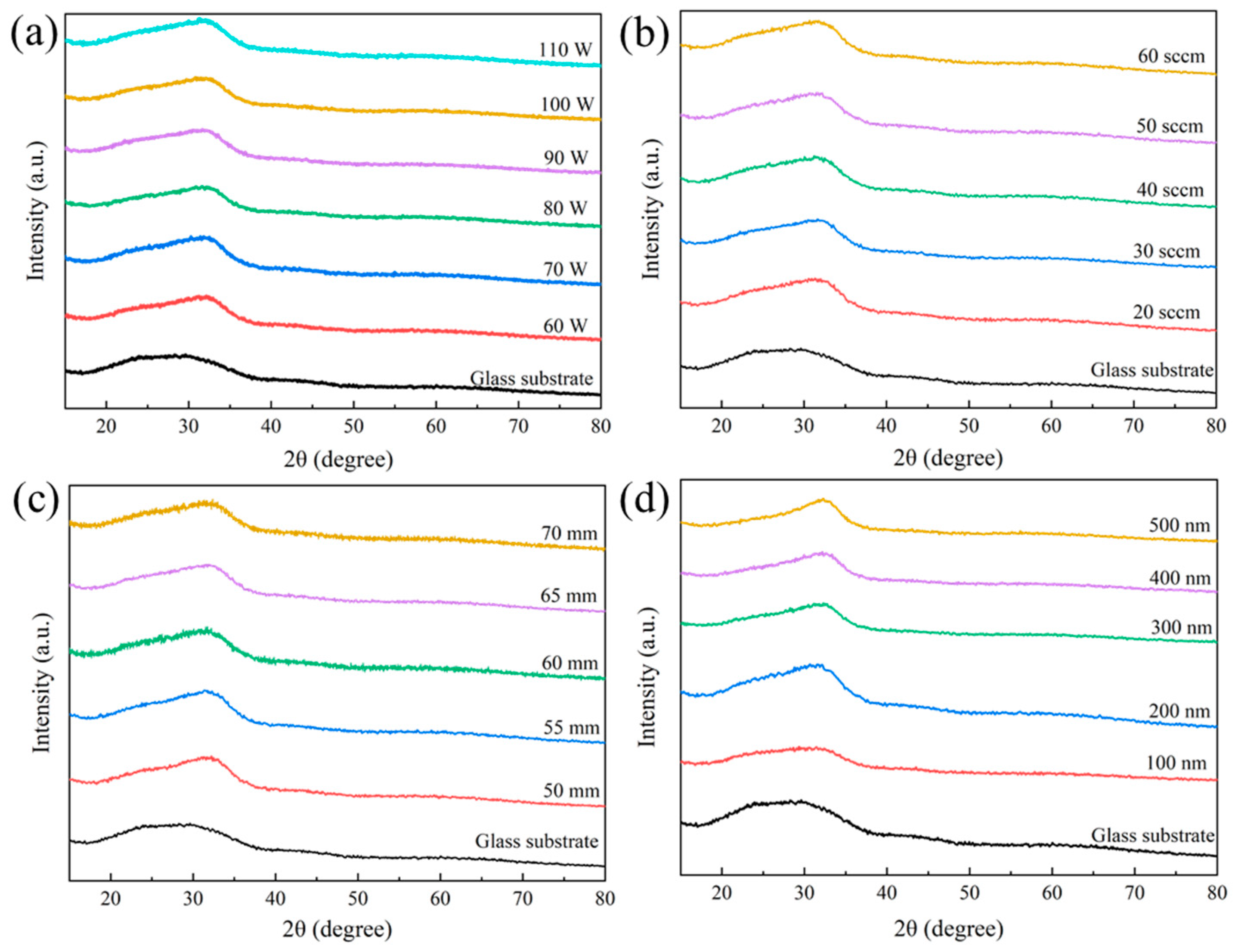
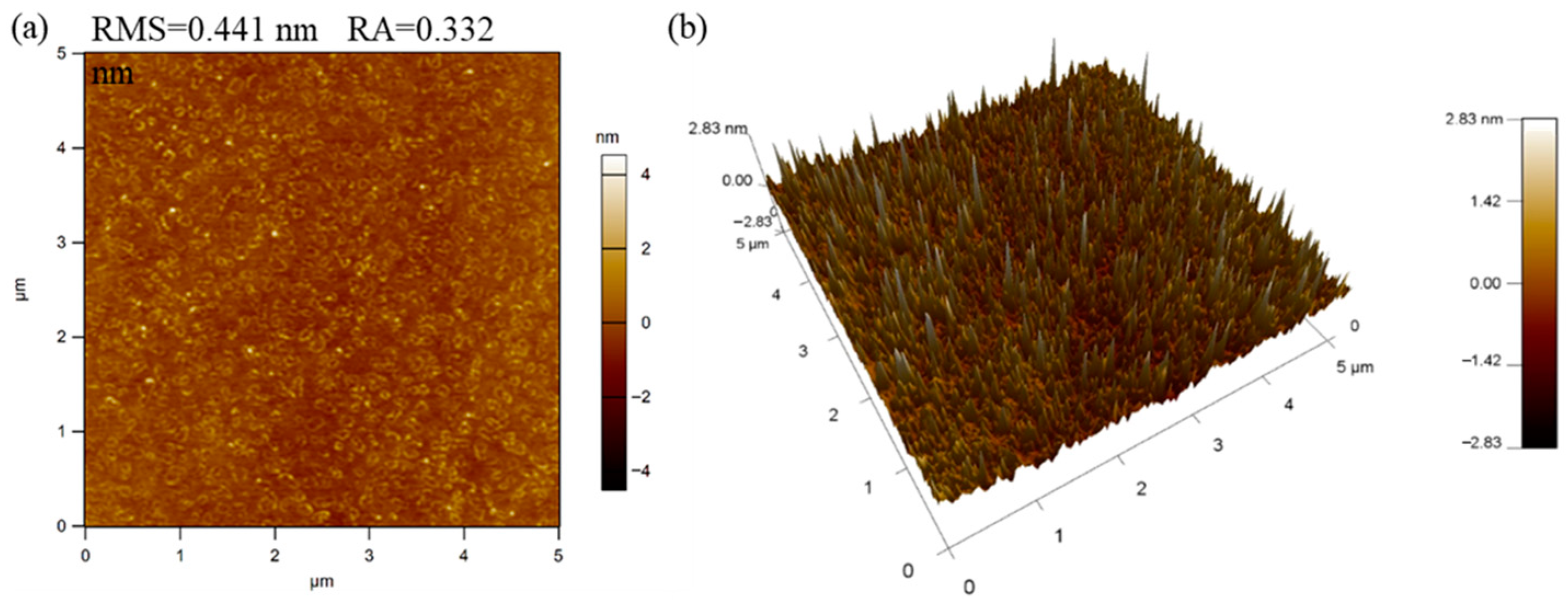
3.1. Structure and Surface Morphology
3.2. Optical Properties
3.2.1. Transmittance Spectra
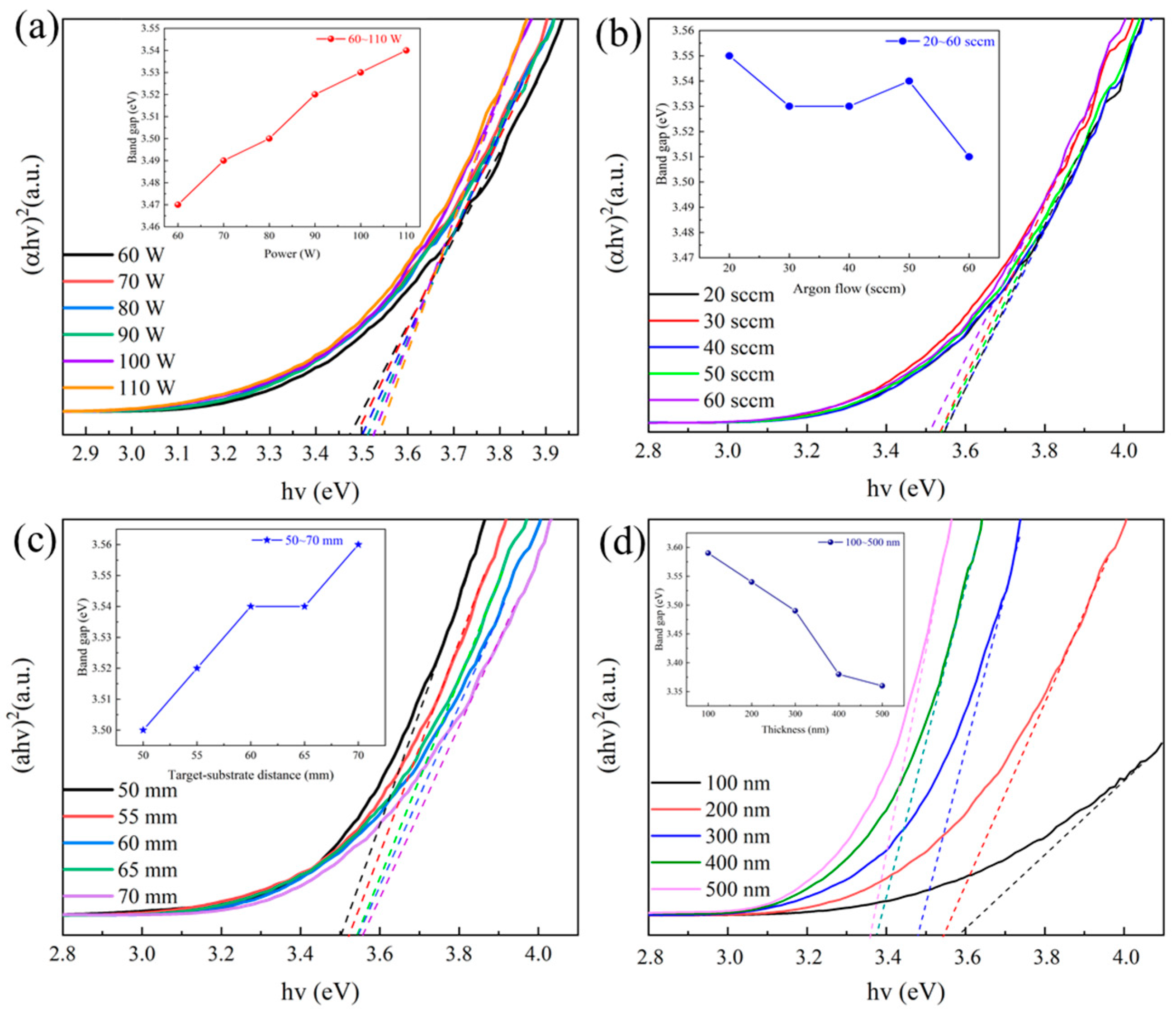
3.2.2. Optical Bandgap
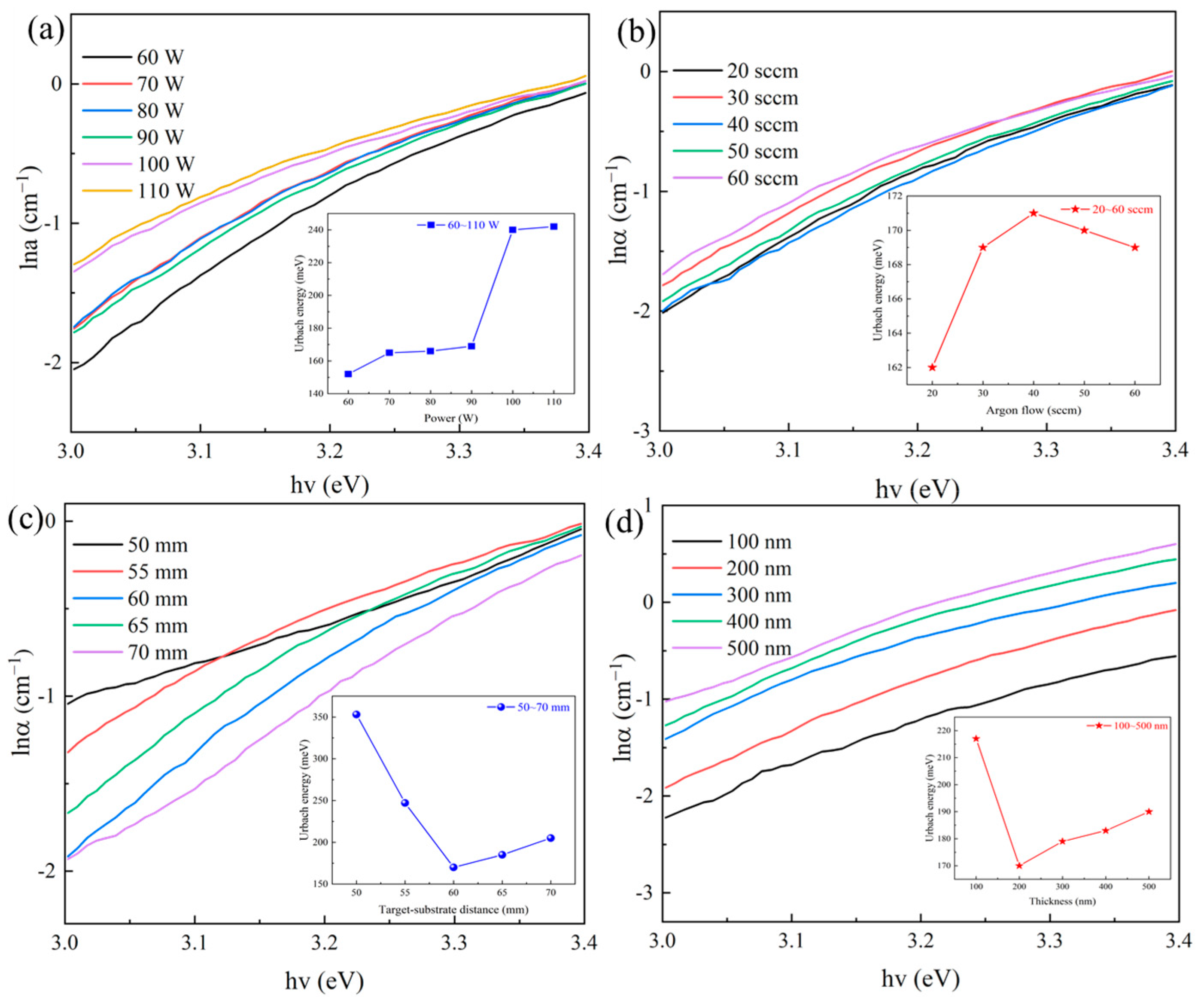
3.2.3. Urbach Energy
3.3. Electrical Properties
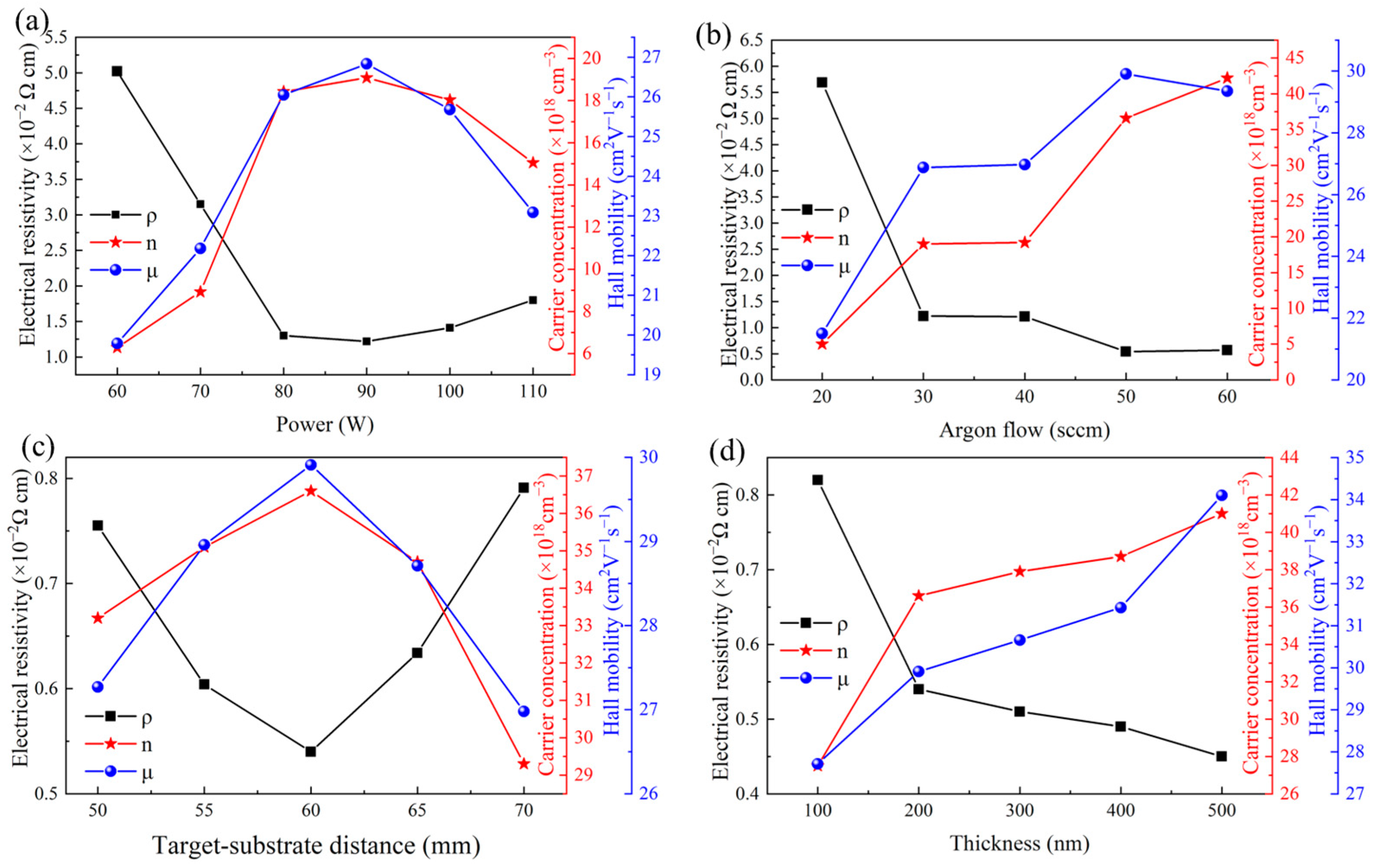
3.3.1. The Effect of Sputtering Power
3.3.2. The Effect of Argon Gas Flow Rates
3.3.3. The Effect of ToSD
3.3.4. The Effect of Film Thickness
3.3.5. Electric Properties Comparison of IGZTO and Previous IGZO or ITZO Films
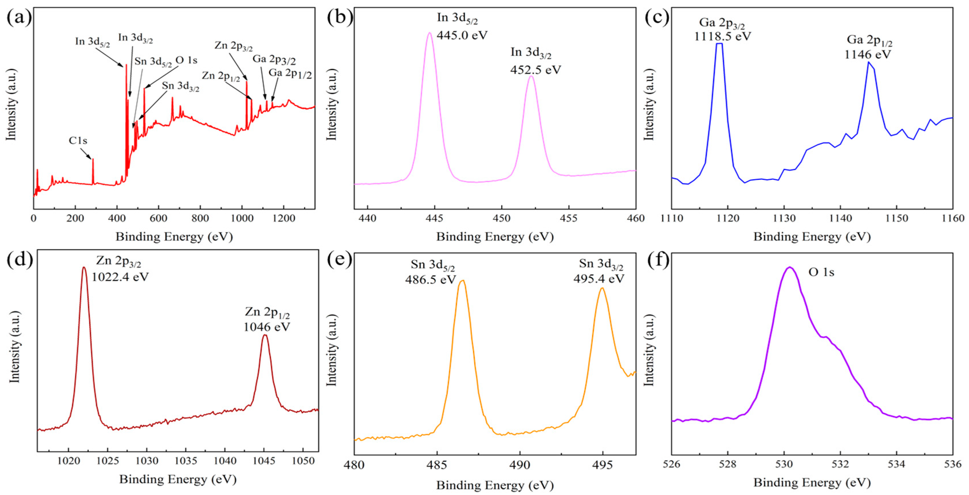
3.4. XPS Analysis of Element Content and Oxygen Vacancies
3.4.1. Element Content of the IGZTO Thin Films
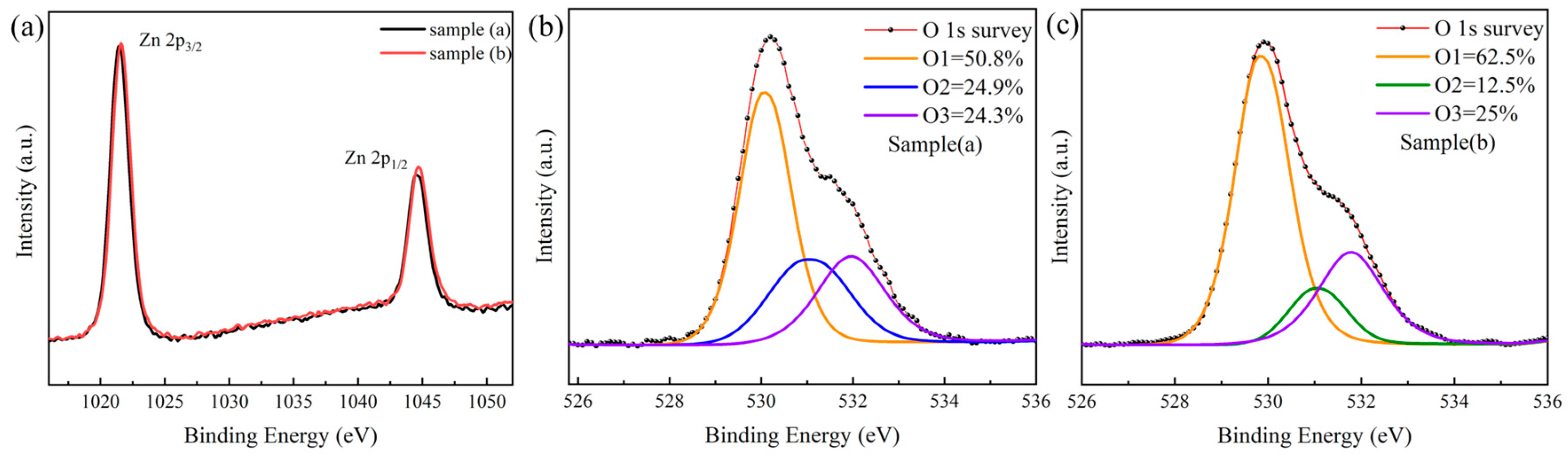
3.4.2. Comparison of Zinc Interstitials in Different Samples
3.4.3. Comparison of Oxygen Vacancies in Different Samples
4. Conclusions
- (1)
- All the obtained IGZTO thin films are amorphous in structure with stable phase characteristics and have a smooth and uniform surface with a low roughness (RMS of 0.441 nm, RA of 0.332 nm).
- (2)
- All the obtained IGZTO thin films are transparent, demonstrating good average visible light transmittance (89.02~90.69%), low Urbach energy (152~353 meV), and an optical bandgap of 3.47~3.56 eV.
- (3)
- The 200 nm thick IGZTO film obtained at 90 W sputtering power, 50 sccm argon gas flow rate, 60 mm target-to-substrate distance exhibits optimal electrical properties with a carrier concentration of 3.66 × 1019 cm−3, Hall mobility of 29.91 cm2/Vs, and resistivity of 0.54 × 10⁻² Ω·cm.
- (4)
- XPS analysis revealed that Zn interstitials exist in the IGZTO films, but its content varies little in different samples, means, Zn interstitials are not the origin of the different electrical properties of various IGZTO films.
- (5)
- XPS analysis indicated that O atoms have three states in IGZTO films: oxygen atoms bonded with metal in the lattice (such as In–O, Ga–O), oxygen vacancies, and adsorbed oxygen species on the surface or interstitial oxygen. Among them, the oxygen-deficient defects act as donors, providing the main carrier. In other word, the electrical properties of IGZTO films are mainly ascribed to the concentration of oxygen vacancies.
Author Contributions
Funding
Institutional Review Board Statement
Informed Consent Statement
Data Availability Statement
Conflicts of Interest
References
- Nomura, K.; Ohta, H.; Takagi, A.; Kamiya, T.; Hirano, M.; Hosono, H. Room-temperature fabrication of transparent flexible thin-film transistors using amorphous oxide semiconductors. Nature 2004, 432, 488–492. [Google Scholar] [CrossRef]
- Shiah, Y.S.; Sim, K.; Shi, Y.; Abe, K.; Ueda, S.; Sasase, M.; Hosono, H. Mobility–stability trade-off in oxide thin-film transistors. Nat. Electron. 2021, 4, 800–807. [Google Scholar] [CrossRef]
- Kim, D.G.; Choi, H.; Kim, Y.S.; Lee, D.H.; Oh, H.J.; Lee, J.H.; Park, J.S. Selectively nitrogen doped ALD-IGZO TFTs with extremely high mobility and reliability. ACS Appl. Mater. 2023, 15, 31652–31663. [Google Scholar] [CrossRef] [PubMed]
- Su, B.Y.; Chu, S.Y.; Juang, Y.D.; Liu, S.Y. Effects of Mg doping on the gate bias and thermal stability of solution-processed InGaZnO thin-film transistors. J. Alloys Compd. 2013, 580, 10–14. [Google Scholar] [CrossRef]
- Kim, H.G.; Lee, H.J.; Lee, K.M.; Kim, T.G. Improved mobility and bias stability of Hf-doped IGZO/IZO/Hf-doped IGZO thin-film transistor. J. Alloys Compd. 2024, 981, 173587. [Google Scholar] [CrossRef]
- Choi, I.M.; Kim, M.J.; On, N.; Song, A.; Chung, K.B.; Jeong, H.; Jeong, J.K. Achieving high mobility and excellent stability in amorphous In-Ga-Zn-Sn-O thin-film transistors. IEEE. Trans. Electron. Dev. 2020, 67, 1014–1020. [Google Scholar] [CrossRef]
- Sun, T.; Shi, L.Q.; Su, C.Y.; Li, W.H.; Lv, X.W.; Zhang, H.J.; Meng, Y.H.; Shi, W.; Ge, S.M.; Tseng, C.Y.; et al. Amorphous indium-gallium-zinc-tin-oxide TFTs with high mobility and reliability. SID Symp. Dig. Tech. Pap. 2015, 46, 766–768. [Google Scholar] [CrossRef]
- Ochi, M.; Morita, S.; Takanashi, Y.; Tao, H.; Goto, H.; Kugimiya, T.; Kanamaru, M. Electrical characterization of BCE-TFTs with a-IGZTO oxide semiconductor compatible with Cu and Al interconnections. SID Symp. Dig. Tech. Pap. 2015, 46, 853–856. [Google Scholar] [CrossRef]
- Zhu, B.; Roach, K.E.; Lynch, D.M.; Chung, C.Y.; Ast, D.G.; Greene, R.G.; Thompson, M.O. Effects of RF sputtering parameters on C-axis aligned crystalline (CAAC) InGaZnO4 films using design of experiment (DOE) approach. ECS J. Solid State Sci. Technol. 2016, 5, 368. [Google Scholar] [CrossRef]
- Lin, T.C.; Huang, W.C.; Lan, W.C. A study on the electrical and optical characteristics of IGZO films. J. Mater Sci-Mater Electron. 2014, 25, 3077–3084. [Google Scholar] [CrossRef]
- Lin, C.Y.; Tang, K.; Leu, C.M.; Yeh, Y.H. Flexible IGZO thin-film transistors and inverter circuits with diode-connected transistors fabricated on transparent polyimide substrates. Microsyst. Technol. 2022, 28, 275–278. [Google Scholar] [CrossRef]
- Wu, C.H.; Chang, K.M.; Huang, S.H.; Deng, I.C.; Wu, C.J.; Chiang, W.H.; Lin, J.W.; Chang, C.C. The effect of thermal annealing on the properties of IGZO TFT prepared by atmospheric pressure plasma jet. ECS Trans. 2012, 45, 189. [Google Scholar] [CrossRef]
- Kim, J.H.; Park, E.K.; Kim, M.S.; Cho, H.J.; Lee, D.H.; Kim, J.H.; Khang, Y.; Park, K.; Kim, Y.S. Bias and illumination instability analysis of solution-processed a-InGaZnO thin-film transistors with different component ratios. Thin Solid Film. 2018, 645, 154–159. [Google Scholar] [CrossRef]
- Kang, M.S.; Cho, W.J. High-performance amorphous indium gallium zinc oxide thin-film transistors with sol-gel processed gate dielectric and channel layer fabricated using microwave irradiation. Curr. Appl. Phys. 2018, 18, 1080–1086. [Google Scholar] [CrossRef]
- Kuo, D.H.; Huang, Y.K.; Hsueh, T.H.; Jan, D.J. Properties optimization with high nitrogen content doping for InGaZnO films deposited by reactive sputtering with a GaN-embedded cermet target. Mater. Sci. Semicond. Process 2018, 86, 122–127. [Google Scholar] [CrossRef]
- Park, B.J.; Chung, S.W.; Kim, M.J.; Lee, H.J.; Bae, J.H.; Kang, S.C.; Jeong, J.K. Achieving high field-effect mobility exceeding 90 cm2/Vs in a-IGZTO transistors with excellent reliability. IEEE Electron. Device Lett. 2023, 44, 1857–1860. [Google Scholar] [CrossRef]
- Yang, T.T.; Kuo, D.H.; Tang, K.P. n-type Sn substitution in amorphous IGZO film by sol-gel method: A promoter of hall mobility up to 65 cm2/V·s. J. Non-Cryst. Solids 2021, 553, 120503. [Google Scholar] [CrossRef]
- Wu, F.; Fang, L.; Pan, Y.J.; Zhou, K.; Huang, Q.L.; Kong, C.Y. Effect of substrate temperature on the structural, electrical and optical properties of ZnO:Ga thin films prepared by RF magnetron sputtering. Phys. E 2010, 43, 228–234. [Google Scholar] [CrossRef]
- Burstein, E. Anomalous optical absorption limit in InSb. Phys. Rev. A 1954, 93, 632–633. [Google Scholar] [CrossRef]
- Moss, T. The interpretation of the properties of indium antimonide. Proc. Phys. Soc. Sect. B 1954, 67, 775. [Google Scholar] [CrossRef]
- Tüzemen, E.Ş.; Eker, S.; Kavak, H.; Esen, R. Dependence of film thickness on the structural and optical properties of ZnO thin films. Appl. Surf. Sci. 2009, 255, 6195–6200. [Google Scholar] [CrossRef]
- He, P.; Hong, R.; Li, G.; Zou, X.; Hu, W.; Lan, L.; Iñíguez, B.; Liao, L.; Liu, X. Effect of humidity on properties of aqueous-processed Tb-doped indium oxide thin-film transistors. IEEE Electron. Device Lett. 2022, 43, 1894–1897. [Google Scholar] [CrossRef]
- He, F.; Wang, Y.; Lin, Z.; Su, J.; Zhang, J.; Chang, J.; Hao, Y. Aqueous solution-deposited aluminum-gallium-oxide alloy gate dielectrics for low voltage fully oxide thin film transistors. Appl. Phys. Lett. 2021, 119, 11. [Google Scholar] [CrossRef]
- Li, S.; Tian, M.; Gao, Q.; Wang, M.; Li, T.; Hu, Q.; Li, X.; Wu, Y. Nanometre-thin indium tin oxide for advanced high-performance electronics. Nat. Mater. 2019, 18, 1091–1097. [Google Scholar] [CrossRef]
- Feneberg, M.; Osterburg, S.; Lange, K.; Lidig, C.; Garke, B.; Goldhahn, R.; Richter, E.; Netzel, C.; Witte, H.; Krost, A. Band gap renormalization and Burstein-Moss effect in silicon-and germanium-doped wurtzite GaN up to 1020 cm−3. Phys. Rev. B 2014, 90, 075203. [Google Scholar] [CrossRef]
- Tavger, B.A.; Demikhovskiĭ, V.Y. Quantum size effects in semiconducting and semimetallic films. Phys. Usp. 1969, 11, 644. [Google Scholar] [CrossRef]
- Mahjabin, S.; Haque, M.M.; Sobayel, K.; Selvanathan, V.; Jamal, M.S.; Bashar, M.S.; Akhtaruzzaman, M. Investigation of morphological, optical, and dielectric properties of RF sputtered WOx thin films for optoelectronic applications. Nanomaterials 2022, 12, 3467. [Google Scholar] [CrossRef]
- Baneto, M.; Enesca, A.; Lare, Y.; Jondo, K.; Napo, K.; Duta, A. Effect of precursor concentration on structural, morphological and opto-electric properties of ZnO thin films prepared by spray pyrolysis. Ceram. Int. 2014, 40, 8397–8404. [Google Scholar] [CrossRef]
- Salem, M.; Alami, Z.Y.; Bessais, B.; Chahboun, A.; Gaidi, M. Structural and optical properties of ZnO nanoparticles deposited on porous silicon for mc-Si passivation. J. Nanopart. Res. 2015, 17, 137. [Google Scholar] [CrossRef]
- Shakiba, M.; Kosarian, A.; Farshidi, E. Effects of processing parameters on crystalline structure and optoelectronic behavior of DC sputtered ITO thin film. J. Mater. Sci.-Mater. Electron. 2017, 28, 787–797. [Google Scholar] [CrossRef]
- Yang, P.; Zhao, X.; Yang, L.; Gu, Y.; Lin, H.; Lai, X. Effect of argon flow rate on photoelectric properties of aluminum-doped zinc oxide thin films. Rare Metal. Mat. Eng. 2018, 47, 91–94. (In Chinese) [Google Scholar]
- Jia, J.; Oka, N.; Kusayanagi, M.; Nakatomi, S.; Shigesato, Y. Origin of carrier scattering in polycrystalline Al-doped ZnO films. Appl. Phys. Express 2014, 7, 105802. [Google Scholar] [CrossRef]
- Rajalakshmi, R.; Angappane, S. Effect of thickness on the structural and optical properties of sputtered ZnO and ZnO: Mn thin films. J. Alloys Compd. 2014, 615, 355–362. [Google Scholar] [CrossRef]
- Trinh, T.T.; Jang, K.; Velumani, S.; Dao, V.A.; Yi, J. Role of Schottky barrier height at source/drain contact for electrical improvement in high carrier concentration amorphous InGaZnO thin film transistors. Mater. Sci. Semicond. Process 2015, 38, 50–56. [Google Scholar] [CrossRef]
- Jeong, J.H.; Yang, H.W.; Park, J.S.; Jeong, J.K.; Mo, Y.G.; Kim, H.D.; Song, J.; Hwang, C.S. Origin of subthreshold swing improvement in amorphous indium gallium zinc oxide transistors. Electrochem. Solid-State Lett. 2008, 11, 157. [Google Scholar] [CrossRef]
- Mridha, S.; Basak, D. Effect of thickness on the structural, electrical and optical properties of ZnO films. Mater. Res. Bull. 2007, 42, 875–882. [Google Scholar] [CrossRef]
- Jayaraman, V.K.; Álvarez, A.M. Effect of substrate temperature on structural, morphological, optical and electrical properties of IGZO thin films. Phys. E 2017, 86, 164–167. [Google Scholar] [CrossRef]
- Zhang, Y.; Chen, J.; Sun, B.S.; Liu, S.; Wang, Z.J.; Liu, S.H.; Shu, Y.C.; He, J.L. Optical and electrical properties of room temperature prepared a-IGZO thin films using an In2Ga2ZnO7 ceramic target. J. Cent. South Univ. 2022, 29, 1062–1074. [Google Scholar] [CrossRef]
- Ding, A.; You, R.; Luo, S.; Gong, J.; Song, S.; Wang, K.; Dai, B.; Sun, H. Influence of annealing temperature on the optoelectronic properties of ITZO thin films. Nanotechnology 2021, 32, 405701. [Google Scholar] [CrossRef]
- Rezek, J.; Houška, J.; Procházka, M.; Haviar, S.; Kozák, T.; Baroch, P. In-Ga-Zn-O thin films with tunable optical and electrical properties prepared by high-power impulse magnetron sputtering. Thin Solid Film. 2018, 658, 27–32. [Google Scholar] [CrossRef]
- Lupan, O.; Emelchenko, G.A.; Ursaki, V.V.; Chai, G.; Redkin, A.N.; Gruzintsev, A.N.; Yakimov, E.E. Synthesis and characterization of ZnO nanowires for nanosensor applications. Mater. Res. Bull. 2010, 45, 1026–1032. [Google Scholar] [CrossRef]
- Das, J.; Pradhan, S.K.; Sahu, D.R.; Mishra, D.K.; Sarangi, S.N.; Nayak, B.B.; Roul, B.K. Micro-Raman and XPS studies of pure ZnO ceramics. Phys. B 2010, 405, 2492–2497. [Google Scholar] [CrossRef]
- Chang, C.S.; Li, T.C.; Tsai, Y.C.; Wu, G.H.; Lin, J.F. Effects of deposition method and conditions for IGZO film and thermal annealing on composite film quality, surface roughness, microstructural defects, and electrical properties of Ti/IGZO/graphene/polyimide specimens. J. Alloys Compd. 2018, 768, 298–315. [Google Scholar] [CrossRef]
- Wu, J.; Shi, J.; Dong, C.; Zou, Z.; Chen, Y.; Zhou, D.; Hu, Z.; Zhan, R. Effect of active layer deposition temperature on the performance of sputtered amorphous In-Ga-Zn-O thin film transistors. J. Semicond. 2014, 35, 014003. [Google Scholar] [CrossRef]
- Rim, Y.S.; Kim, D.L.; Jeong, W.H.; Kim, H.J. Effect of Zr addition on ZnSnO thin-film transistors using a solution process. Appl. Phys. Lett. 2010, 97, 233502. [Google Scholar] [CrossRef]
- Hsieh, P.T.; Chen, Y.C.; Kao, K.S.; Wang, C.M. Luminescence mechanism of ZnO thin film investigated by XPS measurement. Appl. Phys. A 2008, 90, 317–321. [Google Scholar] [CrossRef]
- Yang, S.; Zhang, C.; Yang, Z.; Yao, J.; Wang, H.; Ding, G. Effect of nitrogen doping temperature on the resistance stability of ITO thin films. J. Alloys Compd. 2019, 778, 90–96. [Google Scholar] [CrossRef]
- Xiao, P.; Huang, J.; Dong, T.; Yuan, J.; Yan, D.; Xie, J.; Tan, H. X-ray photoelectron spectroscopy analysis of the effect of photoresist passivation on InGaZnO thin-film transistors. Appl. Surf. Sci. 2019, 471, 403–407. [Google Scholar] [CrossRef]
- Noh, H.K.; Chang, K.J.; Ryu, B.; Lee, W.J. Electronic structure of oxygen-vacancy defects in amorphous In-Ga-Zn-O semiconduc-tors. Phys. Rev. B Condens. Matter Mater. Phys. 2011, 84, 115205. [Google Scholar] [CrossRef]
- Janotti, A.; Van de Walle, C.G. Oxygen vacancies in ZnO. Appl. Phys. Lett. 2005, 87, 12. [Google Scholar] [CrossRef]
- Sun, H.; Jen, S.U.; Chiang, H.P.; Chen, S.C.; Lin, M.H.; Chen, J.Y.; Wang, X. Investigation of optoelectronic performance in In, Ga co-doped ZnO thin films with various In and Ga levels. Thin Solid Film. 2017, 641, 12–18. [Google Scholar] [CrossRef]


| Variable Series | Sputtering Power (W) | Argon Flow (sccm) | ToSD (mm) | Film Thickness (nm) | |
|---|---|---|---|---|---|
| Same thickness | Sputtering power | 60, 70, 80, 90, 100, 110 | 30 | 60 | 200 |
| Argon flow | 90 | 20, 30, 40, 50, 60 | 60 | 200 | |
| ToSD | 90 | 50 | 50, 55, 60, 65, 70 | 200 | |
| Different thickness | 90 | 50 | 60 | 100, 200, 300, 400, 500 | |
| Thin Film | Method | Carrier Concentration (cm−3) | Hall Mobility (cm2/Vs) | Electrical Resistivity (Ω·cm) | Average Visible Light Transmittance | Eg (eV) | Ref. |
|---|---|---|---|---|---|---|---|
| IGZO | MS * | / | 7.7 | / | / | / | [7] |
| IGZTO | MS | / | 12.2 | / | / | / | [7] |
| Ga: IZO | Mc-S * | 1.8 × 10²⁰ | 29 | 3.0 × 10⁻³ | 86.5% | 3.40 | [10] |
| IGZTO | Sol–gel | 3.48 × 10¹⁵ | 65 | 27.78 | 89% | 3.66 | [17] |
| IGZO | SP * | / | / | 1.05 × 10⁻² | >70% | 3.39 | [37] |
| IGZO | MS | / | / | 3.4 × 10⁻² | 91.93% | 3.79 | [38] |
| ITZO | MS | 1.27 × 10²⁰ | 24.31 | / | 89.87% | 3.74 | [39] |
| IGZTO [This work] | MS | 3.66 × 10¹⁹ | 29.91 | 0.54 × 10⁻² | 90.21% | 3.54 | / |
| Peak Name | Binding Energy (eV) | Meaning | Area Percentage of Peak (Area%) | |
|---|---|---|---|---|
| Sample (a) | Sample (b) | |||
| O1 | 530.0 ± 0.2 | Oxygen atoms bonded in the lattice [43,44], such as Zn-O and In-O [45]. | 50.8 | 62.5 |
| O2 | 531.0 ± 0.1 | Oxygen vacancies (Vo) [46]. | 24.9 | 12.5 |
| O3 | 532.0 ± 0.3 | Adsorbed oxygen species on the film surface [47], such as O2, H2O, –CO3, and –OH groups [48]. | 24.3 | 25 |
| Carrier concentration | / | / | 3.66 × 1019 cm−3 | 5.0 × 1018 cm−3 |
Disclaimer/Publisher’s Note: The statements, opinions and data contained in all publications are solely those of the individual author(s) and contributor(s) and not of MDPI and/or the editor(s). MDPI and/or the editor(s) disclaim responsibility for any injury to people or property resulting from any ideas, methods, instructions or products referred to in the content. |
© 2025 by the authors. Licensee MDPI, Basel, Switzerland. This article is an open access article distributed under the terms and conditions of the Creative Commons Attribution (CC BY) license (https://creativecommons.org/licenses/by/4.0/).
Share and Cite
Wu, H.; Fang, L.; Li, Z.; Wu, F.; Zhang, S.; Liu, G.; Zhang, H.; Li, W.; Feng, W. Fabrication and Optoelectronic Properties of Advanced Quinary Amorphous Oxide Semiconductor InGaZnSnO Thin Film. Materials 2025, 18, 2090. https://doi.org/10.3390/ma18092090
Wu H, Fang L, Li Z, Wu F, Zhang S, Liu G, Zhang H, Li W, Feng W. Fabrication and Optoelectronic Properties of Advanced Quinary Amorphous Oxide Semiconductor InGaZnSnO Thin Film. Materials. 2025; 18(9):2090. https://doi.org/10.3390/ma18092090
Chicago/Turabian StyleWu, Hongyu, Liang Fang, Zhiyi Li, Fang Wu, Shufang Zhang, Gaobin Liu, Hong Zhang, Wanjun Li, and Wenlin Feng. 2025. "Fabrication and Optoelectronic Properties of Advanced Quinary Amorphous Oxide Semiconductor InGaZnSnO Thin Film" Materials 18, no. 9: 2090. https://doi.org/10.3390/ma18092090
APA StyleWu, H., Fang, L., Li, Z., Wu, F., Zhang, S., Liu, G., Zhang, H., Li, W., & Feng, W. (2025). Fabrication and Optoelectronic Properties of Advanced Quinary Amorphous Oxide Semiconductor InGaZnSnO Thin Film. Materials, 18(9), 2090. https://doi.org/10.3390/ma18092090