Abstract
Mixed-halide perovskites enable the creation of high-performance and low-cost solar cells. Chloride incorporation enhances film morphology, carrier diffusion length, and stability, improving device performance. Nevertheless, optimizing film thickness, defect density, and metal contact work function remains insufficiently explored, despite its potential to enhance power conversion efficiency. In this study, a numerical simulation was performed using SCAPS-1D (version 3.3.10) to identify the optimal parameters for the FTO/TiO2/CH3NH3Pb3−xClx/Spiro-OMeTAD/Au configuration. The best performance parameters that have been published in the literature based on experimental results are as follows: VOC = 1.077 V, JSC = 21.45 mA/cm2, FF = 77.57%, and PCE = 17.97%. In contrast, the performance parameters obtained from numerical simulations for the same structure are VOC = 1.28 V, JSC = 21.63 mA/cm2, FF = 78%, and PCE = 21.53%. In our numerical analysis, we achieved efficiencies that were comparable to those reported in experimental studies, and after optimization, superior performance parameters were attained, including VOC = 1.179 V, JSC = 27.26 mA/cm2, FF = 81.03%, and PCE = 26.07%. These results indicate that optimized parameters can be integrated into the design and fabrication of mixed-halide perovskite solar cells to enhance performance.
1. Introduction
Fossil fuels such as coal, oil, and natural gas and are the most abundant and widely used energy sources for electricity production. The sustained utilization of these fuels has a significant impact on climate change and global warming [1]. Consequently, this has led to the use of alternative energy sources, especially renewable energies. In this context, solar energy is considered one of the most promising clean energy sources for the future due to its availability, purity, and inexhaustibility. Moreover, the use of solar energy is environmentally friendly [2]. Considering the global demand for sustainable energy solutions, perovskite solar cells (PSCs) have demonstrated noteworthy potential as photovoltaic technology due to their low costs, simple fabrication methods, and high efficiencies. Additionally, it should be noted that since their introduction, the power conversion efficiency (PCE) of PSCs has increased from 3.8% in 2009 to 25.6% within a comparatively small period [3,4].
The structure of perovskite materials is typically composed of three elements, with a general formula of ABX3, where A represents a monovalent organic, inorganic, or mixed cation such as methylammonium (MA+), formamidinium (FA+), or caesium (Cs+). B is a divalent cation, commonly lead (Pb2⁺) or tin (Sn2⁺), and X is a halide such as iodide (I⁻), bromide (Br⁻), or chloride (Cl⁻). Perovskite materials exhibit excellent properties, such as low exciton binding energy, long-range ambipolar charge transport, high absorption coefficients, long diffusion lengths, tuneable energy bandgaps, and low-temperature synthesis. These attributes make it an appropriate option for diverse optoelectronic devices, including photodetectors, LEDs, sensors, and solar cells [5].
MAPbX3 is the most widely used and studied perovskite material in PSCs for solar cell applications. Nevertheless, it has limited stability and environmental concerns restrict its applications [6]. Previous studies have shown that the incorporation of Cl⁻ in CH3NH3PbI3 perovskite improves the stability and crystallinity [7]. It has also been reported that the carrier lifetime, diffusion coefficient, and diffusion length are higher in mixed-halide perovskite (CH3NH3PbI3−xClx) compared to conventional perovskite (CH3NH3PbI3). The result is a better accumulation of charge carriers. This improves the performance of the fabricated device. Therefore, incorporating Cl⁻ ions into the perovskite is favourable for improving both stability and efficiency [8,9].
To enhance the PSCs efficiency, it is crucial to understand their structural design mechanisms. This can be achieved through the implementation of numerical simulations, using specialized simulation software programs [10]. Consequently, a comprehensive analysis of performance parameters, including power conversion efficiency (PCE), fill factor (FF), short-circuit current density (JSC), and open-circuit voltage (VOC), is imperative. This analysis should encompass changes in layer thickness, defect densities, series and parallel resistances, operating temperature, and the work function of the metal contact, to achieve high efficiency.
In this article, we simulated and optimized a PSCs (FTO/TiO2/CH3NH3PbI3−xClx/Spiro-OMeTAD/Au) using the SCAPS-1D software version 3.3.10. In the structure, Spiro-OMeTAD and TiO2 serve as the hole and electron transport layers (HTL and ETL, respectively). Although inorganic materials can be used as HTLs, which have advantages in their application such as stability, availability, and lower cost, this type of material shows significantly lower efficiency compared to HTLs made of organic materials. The most prominent organic HTLs are poly(3-hexylthiophene-2,5-diyl) (P3HT), poly[bis(4-phenyl) (2,4,6-trimethylphenyl) amine] (PTAA), PEDOT: PSS, and Spiro-OMeTAD. While all these materials have demonstrated promising results when they are used as HTLs, the best structures in terms of efficiency achieved (with efficiencies greater than 25%) are those that incorporate Spiro-OMeTAD [11].
In the context of organic ETLs, these materials typically exhibit an optimal alignment of the work function. However, their low conductivity requires the utilization of thin films with thicknesses less than 10 nm to achieve optimal performance, thereby limiting their large-scale application. In contrast, inorganic ETLs offer distinct advantages, including a low work function, stability, and cost-effectiveness in production. However, these materials are also characterized by an important number of surface defects, which cause interfacial problems with the active layer, resulting in a high recombination rate and series resistance [12]. Consequently, TiO2 emerges as a promising candidate for use as an ELT due to its inherent properties, including high mobility, excellent stability, and a wide band gap that facilitates charge separation. This material also exhibits a low trap density, further reducing the issues [13].
The simulation was performed by first optimizing the thicknesses of the absorbent layer, ETL, and HTL. Subsequently, we optimized the defect density in the absorber layer and the interfaces (ETL/Perovskite and Perovskite/HTL). Finally, the series and shunt resistances, work function of the metal contact, and the operating temperature were optimized. These results indicated that the key parameters for improving the performance of the mixed-halide PSC were the perovskite thickness, bulk defects in the perovskite, interfacial defects at ETL/Perovskite, and the work function of the metal contact. The proposed device FTO/TiO2/CH3NH3PbI3−xClx/Spiro-OMeTAD/Au achieved final performance parameters in the simulation of VOC = 1.179 V, JSC = 27.26 mA/cm2, FF = 81.03%, and PCE = 26.07%. These results were compared with experimental and simulation data, demonstrating that our optimized proposed structure exhibited superior performance. Finally, we obtained the J–V current density–voltage curve and the energy band diagram of the initial vs. optimized structure.
2. Materials and Methods
2.1. Solar Cell Structure
Figure 1a and Figure 1b illustrate the configuration and alignment of energy levels for the mixed-halide perovskite solar cell (FTO/TiO2/CH3NH3PbI3−xClx/Spiro-OMeTAD/Au), respectively. In the proposed design, fluorine-doped tin oxide (FTO) serves as the transparent conductive oxide (TCO) and functions as the front electrode; titanium dioxide (TiO2) acts as the electron transport layer (ETL); the mixed-halide perovskite material (CH3NH3PbI3−xClx) serves as the absorber layer; Spiro-OMeTAD functions as the hole transport layer (HTL); and gold (Au) is used as the back metal contact. In the structure, the generation of electron–hole pairs occurs in the perovskite absorber layer, which is responsible for generating the electric current. The photogenerated electrons are transported from the absorber layer to the ETL layer and collected by the FTO front contact. Similarly, the holes are transported from the absorber through the HTL layer and then collected by the gold electrode or back metal contact [14]. Additionally, Figure 1b illustrates the correct alignment of the energy levels of the materials in the PSC. According to the diagram, electrons tend to move to lower energy levels. The ETL has the lowest unoccupied (LUMO) and highest occupied (HOMO) molecular orbitals at lower energy levels compared to the perovskite. In contrast, the LUMO and HOMO of the HTL are located at higher energy levels than those of the perovskite, as shown in Figure 1b.
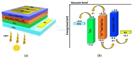
Figure 1.
(a) Schematic diagram of the perovskite device structure and (b) energy bands alignment of the TCO, ETL, absorber, HTL, and back metal contact.
2.2. Basic Equations and Numerical Parameters
The simulation was performed using the one-dimensional solar cell capacitance simulator, SCAPS-1D, developed at the Department of Electronics and Information Systems (ELIS), Ghent University (Belgium). The software can solve the fundamental semiconductor equations in one dimension under steady-state conditions, including Poisson’s equation, continuity equations for electrons and holes, charge transport equations for electrons and holes, and the absorption coefficient [15,16,17]. The SCAPS-1D simulation is based on the following equations:
- Poisson’s equation:
- 2.
- Continuity equations for electrons and holes:
- 3.
- Charge transport equations for electrons and holes:
- 4.
- Absorption coefficient:
The optical and electrical parameters of the PSC materials were gathered from the scientific literature and are summarized in Table 1. Subsequently, Table 2 presents the defect density parameters and the electrical parameters of the back metal contact. The standard solar spectrum AM1.5 G was used for this simulation at 300 K.

Table 1.
Parameters of the different materials used for simulation.
Table 2.
Parameters for defects and back metal contact used for simulation.
3. Results and Discussion
3.1. The Perovskite Absorption Coefficient
The absorption coefficient of the mixed-halide perovskite was experimentally determined and incorporated into the SCAPS-1D software. Figure 2 illustrates the absorption coefficient as a function of wavelength for the mixed-halide perovskite, while inset shows the absorption coefficient as a function of energy. It is evident that absorption is higher at shorter wavelengths (400 nm to 490 nm) and decreases at longer wavelengths (500 nm to 800 nm), with the peak observed at 730 nm.
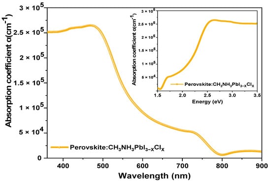
Figure 2.
Experimental absorption coefficient for mixed-halide perovskite.
3.2. Impact of the Perovskite Layer Thickness
The optimization of the perovskite thickness is essential because this is where light absorption and electron–hole pair generation occur. The variation of PCE with perovskite thickness is defined by increased absorption and the recombination rate. If the thickness is small, most of the incident light is transmitted. Therefore, increasing the thickness improves the absorption of the incident light, which results in a higher number of photogenerated carriers. However, if the thickness is too large, these photogenerated charge carriers must travel a longer distance, increasing the recombination rate and decreasing the lifetime of the carriers [35]. The decrease in VOC and PCE is mainly attributed to the increase in dark saturation current, which enhances carriers’ recombination when the thickness is too small or exceeds its optimum value. This behaviour can be explained by the dependence of the open-circuit voltage on the photogenerated current and the dark saturation current, as described by the following Equation (7) [36].
where is the thermal voltage, is the photo-generated current density, and is the saturation current density.
Figure 3 shows the analysis of the effect of the absorber layer thickness on the performance parameters of the perovskite solar cell.
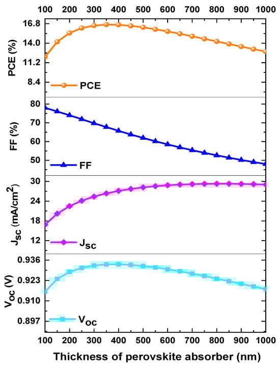
Figure 3.
Variation of PCE, FF, VOC, and JSC as a function of the perovskite layer thickness of mixed halides.
The perovskite thickness was varied from 100 to 1000 nm while keeping the other parameters constant during the simulation. Figure 3 shows the PCE, FF, JSC, and VOC as a function of the mixed-halide perovskite thickness. It was observed that the performance parameter PCE initially increased from 11.94% to 16.67% when the perovskite thickness changed from 100 to 350 nm. However, as the thickness was further increased (from 350 to 1000 nm), the PCE decreased from 16.67% to 12.89%. Meanwhile, the FF continuously decreased from 78.38% to 48.11%, while the JSC consistently increased from 16.54 mA/cm2 to 29.53 mA/cm2. Finally, the VOC increased from 0.9154 V to 0.9332 V as the thickness increased from 100 to 350 nm, after which it saturated and tended to slowly decrease when the thickness exceeded 350 nm, as shown in Figure 3. The optimized thickness of the mixed-halide perovskite in our analysis was 350 nm, and high-performance values were achieved.
3.3. Impact of the TiO2 Layer Thickness
The ETL layer plays a crucial role in the performance of the perovskite solar cell, this layer not only transports electrons but also performs the following functions: (i) it acts as a scaffold for the perovskite layer, (ii) it blocks ultraviolet light from reaching the perovskite, (iii) it blocks hole transport, and (iv) it facilitates exciton dissociation at the TiO2/perovskite interface [37]. In this section, the effect of the TiO2 layer thickness on the performance parameters of the solar cell was analysed. The TiO2 thickness was varied from 10 to 100 nm while keeping the other parameters constant during the simulation. The results, depicted in Figure 4a, reveal the dependence of the PCE, FF, JSC, and VOC as a function of the TiO2 layer thickness.
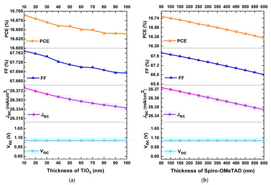
Figure 4.
Variation of PCE, FF, VOC, and JSC as a function of (a) TiO2 thickness and (b) Spiro-OMeTAD thickness.
As illustrated in Figure 4a, a reduction in PCE from 16.69% to 16.64%, FF from 67.77% to 67.69%, and JSC from 26.37 mA/cm2 to 26.33 mA/cm2 was observed, while the VOC value remained constant as the ETL thickness varied from 10 to 100 nm. It was observed that there were no significant changes in PCE, FF, JSC, and VOC as the TiO2 thickness increased. As the thickness of the TiO2 layer increases, the diffusion length and electron mobility decrease due to the higher defect density associated with the increased thickness, resulting in reduced JSC and FF values. Furthermore, as the TiO2 thickness increases, the irradiance on the perovskite absorber decreases. Consequently, lower irradiance on the perovskite absorber reduces the photogeneration of electron–hole pairs, leading to lower JSC and PCE values [38]. Therefore, an optimal ETL thickness of 45 nm was considered in our analysis, which provides optimal performance and meets the minimum thickness that can be experimentally deposited for this layer.
3.4. Impact of the Spiro-OMeTAD Layer Thickness
This section investigates the impact of HTL thickness on the performance parameters of the perovskite solar cell. High-efficiency PSCs typically incorporate Spiro-OMeTAD doped with lithium salts to enhance hole conductivity, with Spiro-OMeTAD deposited using the spin coating method. [39]. Generally, the HTL cannot absorb photons over a wide range like the perovskite layer, so the VOC value does not vary with changes in thickness and remains constant. It has been reported that the use of a thin layer of Spiro-OMeTAD leads to a significant enhancement in the FF value. This is attributed to the fact that holes require less travel distance, thereby reducing the impact of Spiro-OMeTAD conductivity on the device performance. However, it has been reported that devices with thin Spiro-OMeTAD layers exhibit reduced reproducibility, attributable to diminished uniformity of coverage on the rough perovskite layer. This allows for occasional direct contact between the perovskite and Au. As a result, these direct contacts increase the recombination rate of charge carriers, negatively impacting the efficiency of the solar cell [40]. In this section, the thickness of the HTL layer was varied from 50 to 600 nm, while keeping all other parameters constant throughout the simulation. Figure 4b illustrates the variations in PCE, FF, JSC, and VOC as a function of the Spiro-OMeTAD layer thickness. Figure 4b illustrates a decrease in the PCE, FF, and JSC values as the HTL thickness varies from 50 to 600 nm. For instance, the PCE value decreased from 16.78% to 16.35%, the FF decreased from 68.16% to 66.51%, and the JSC decreased from 26.37 mA/cm2 to 26.34 mA/cm2, while the VOC value remained constant. Given these results, there were no significant changes in PCE, FF, and JSC values as the thickness increased. Therefore, in our analysis, an optimal HTL layer thickness of 180 nm was considered, which provides the best performance parameters and represents the minimum thickness that can be experimentally deposited for this layer.
3.5. Impact of the Perovskite Layer Defect Density
One crucial factor in PSC research is the quality of the perovskite absorber layer. High density defects in the perovskite generate recombination centres, reducing the minority carrier lifetime and the carrier diffusion length, which ultimately decreases the power conversion efficiency [41,42]. On the other hand, maintaining a controlled deposition process for the perovskite layer prevents impurities and the formation of deep traps, thereby reducing the total defect density (Nt). Consequently, it is advisable to consider low values of Nt to achieve high device performance [43]. The defect density in the bulk of the perovskite is based on the Shockley–Read–Hall (SRH) recombination model, described by Equation (8) below [44].
where represents the electron concentration, represents the hole concentration, is the intrinsic carrier density, is the energy level of the defect density, and denotes the carrier lifetime.
As a result, the SRH model shows that an increase in carrier lifetime can reduce the recombination rate. The minority carrier lifetime () and the carrier diffusion length () can be obtained using Equations (9) and (10) [29].
where represents the mobility of electrons and holes, respectively, is the capture cross-sectional area for electrons and holes, is the thermal velocity of the carriers, and is the total defect density. As indicated these equations, an increase in within the perovskite bulk leads to the formation of recombination centres in the perovskite solar cell, which reduces the carrier diffusion length and decreases the carrier lifetime. Consequently, this directly impacts the reduction of the VOC and PCE values of the PSC [45].
In this section, the total defect density () of the mixed-halide perovskite was varied from 1010 a 1020 cm−3 while maintaining constant the other parameters during the simulation. Figure 5a presents the PCE, FF, JSC, and VOC as a function of in the perovskite layer. As observed in Figure 5a, there is a decrease in the values of PCE, FF, JSC and VOC as increases. For instance, PCE decreased from 18.57% to 0.02%, FF decreased from 73.08% to 29.35%, JSC decreased from 26.85 mA/cm2 to 0.101 mA/cm2, and VOC decreased from 0.946 V to 0.472 V when varied from 1014 cm−3 to 1020 cm−3. Furthermore, Figure 5b confirms that improved J–V curve output values can be obtained when is less than or equal to 1014 cm−3. Therefore, the optimal value of considered for the perovskite layer was 1014 cm−3.
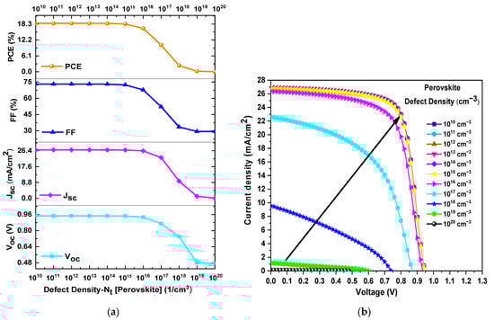
Figure 5.
(a) Variation of PCE, FF, VOC, and JSC as a function of the Nt of the perovskite layer and (b) J–V curves obtained from the Nt variation of the perovskite layer.
3.6. Impact of the Defect Density of the Interfaces: TiO2/CH3NH3PbI3−xClx and CH3NH3PbI3−xClx/Spiro-OMeTAD
The defect density at the interfaces also plays a crucial role in determining the performance of PSCs. The primary causes of defects at the interfaces (TiO2/CH3NH3PbI3−xClx and CH3NH3PbI3−xClx/Spiro-OMeTAD) are associated with chemical impurities, uncoordinated atoms, dangling bonds, and surface dislocations that form on the perovskite surface during the deposition process [46]. Consequently, these defects act as recombination centres at the interfaces, degrading the performance parameters of PSCs [47]. The Shockley–Read–Hall (SRH) recombination for interface defects is determined by the surface recombination velocities of electrons and holes ( and ). Therefore, the recombination rate at the interface can be expressed by Equation (11) [30].
where and represent the concentrations of electrons and holes trapped at the interface, and and are the surface recombination velocities of electrons and holes, respectively.
The recombination at interface states is assessed based on the Paulwels–Vanhoutte theory, which extends the Shockley–Read–Hall (SRH) theory. The determination of recombination states at an interface can be achieved through a similar approach to that employed for the bulk of the perovskite. An ideal interface would minimize interfacial recombination losses (low values of and ), improving device performance [48].
In this section, the total defect density () at the interfaces was varied from 101⁰ to 102⁰ cm⁻2 while keeping the other parameters constant during the simulations. Figure 6a exhibits the PCE, FF, JSC, and VOC as a function of at the TiO₂/CH₃NH₃PbI3−xClₓ interface. Figure 6a shows that the values of PCE, FF, JSC, and VOC decreased as the value of increased. For instance, PCE decreased from 18.41% to 13.89%, FF decreased from 69.04% to 63.24%, JSC decreased from 26.732 mA/cm2 to 24.152 mA/cm2, and VOC decreased from 0.9920 V to 0.9096 V when varied from 1013 cm⁻2 to 102⁰ cm⁻2. Additionally, Figure 6b demonstrates that improved output values from the current density–voltage (J–V) curve are achieved when the value is equal to or less than 1013 cm⁻2. Consequently, the optimum value of for the TiO₂/CH₃NH₃PbI3−xClₓ interface is when it has a value of 1013 cm−2.

Figure 6.
(a) Variation of PCE, FF, VOC, and JSC as a function of Nt of the TiO2/CH3NH3PbI3−xClx interface and (b) J–V curves obtained from the Nt variation of the interface.
Figure 7a displays the PCE, FF, JSC, and VOC as a function of at the CH3NH3PbI3−xClx/Spiro-OMeTAD interface. It is evident from Figure 7a that there is a minimal decrease in the values of PCE, FF, JSC, and VOC as increases. For instance, PCE decreased from 16.74% to 16.45%, FF decreased from 67.94% to 67.30%, JSC decreased from 26.387 mA/cm2 to 26.211 mA/cm2, and VOC decreased from 0.933 V to 0.932 V when varied from 1013 cm−2 a 1020 cm−2. Furthermore, Figure 7b confirms that there is no significant change in the J–V curves when the value of increases or decreases. Therefore, the variation in the value at this interface does not introduce a significant change in the device performance parameters. However, it is noteworthy that the optimal value for the CH3NH3PbI3−xClx/Spiro-OMeTAD interface is when it has a value of 1013 cm−2.
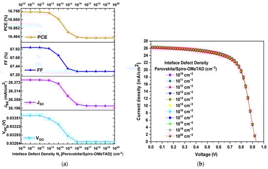
Figure 7.
(a) Variation of PCE, FF, VOC, and JSC as a function of Nt of the CH3NH3PbI3−xClx/Spiro-OMeTAD interface and (b) J–V curves obtained from the Nt variation of the interface.
3.7. Impact of the Series Resistance (Rseries) and Shunt Resistance (Rshunt)
The series resistance (Rseries) and the shunt resistance (Rshunt) have been demonstrated to have a significant impact on the efficiency of mixed-halide PSCs. These resistances determine the appearance and slope of the J–V characteristic plot. Rseries originates from the electrical resistance associated with the contacts (FTO and Au) and the electrical dissipation occurring in the ETL, HTL, and perovskite layers [28]. In addition, Rshunt is associated with the manifestation of various recombination pathways and defects introduced during the film deposition process. Achieving a low Rseries value and a high Rshunt value is essential for obtaining efficient PSCs [49]. Figure 8 shows the equivalent circuit of the perovskite solar cell under illumination. This circuit includes a current source associated with the lighting, a current source to perform charge separation (current generated by the diode), a series resistance (Rseries), and a shunt resistance (Rshunt).
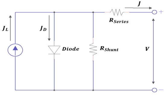
Figure 8.
Equivalent electrical circuit diagram of a perovskite solar cell.
The J–V characteristic of the equivalent circuit can be expressed by Equation (12), which describes the influence of Rseries and Rshunt on the performance of the solar device [43].
where is the current through the external circuit, is the light-induced current density, is the saturation current density, is the output voltage, is the ideality factor, is the Boltzmann constant, is the temperature in Kelvin, and is the electron charge. In an open-circuit condition ( mA/cm2), VOC and Rshunt are expressed through equation (13).
Consequently, a high value of Rseries will mainly affect the FF and JSC values, while a low value of Rshunt causes a loss of photovoltage and will affect the collected photocurrent [23].
In this section, the effect of varying the values of Rseries and Rshunt on the performance parameters of mixed-halide PSCs was observed. Rseries was varied from 0 to 100 , while Rshunt was varied from 500 to 5000 . Figure 9a and Figure 9b illustrate the PCE, FF, JSC, and VOC as a function of Rseries and Rshunt, respectively.
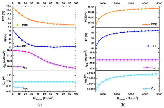
Figure 9.
Variation of PCE, FF, VOC, and JSC as a function of (a) Rseries and (b) Rshunt.
Regarding Rseries, PCE decreased from 16.67% to 2.01%, FF decreased from 67.75% to 24.53%, JSC decreased from 26.36 mA/cm2 to 8.78 mA/cm2, and VOC remained constant at a value of 0.9335 V when Rseries varied from 0 to 100 , as shown in Figure 9a. For Rshunt, PCE increased from 15.58% to 16.56%, FF increased from 64.3% to 67.42%, JSC remained constant at a value of 26.365 mA/cm2, and VOC increased from 0.9188 V to 0.9317 V when Rshunt varied from 500 to 5000 , as shown in Figure 9b. As a result, the optimal values considered to achieve high performance are when Rseries and Rshunt have values of 1 and 5000 , respectively.
3.8. Impact of the Operating Temperature and Metallic Contact Work Function
The operating temperature of the device plays a crucial role in the performance of mixed-halide PSCs. It is well-documented that perovskite exhibits degradation under conditions of elevated temperature and humidity. Furthermore, an increase in temperature induces deformations at the interfaces, leading to the formation of defects and, consequently, the creation of recombination centres. This phenomenon contributes to a reduction in the carrier diffusion length and lifetime. Additionally, an increase in temperature decreases the interconnectivity between layers [50]. These factors directly affect the VOC and PCE. As the temperature rises, the short-circuit current density (JSC) remains relatively constant; however, the VOC gradually decreases, thereby deteriorating the characteristics of the J–V curve. Consequently, the progressive reduction in VOC leads to a decline in the PCE value. Therefore, temperature variations directly influence the performance of PSCs through VOC [45,51]. The correlation between VOC and T is given by equation (14) below [45].
In this equation, denotes the operating temperature, is the energy bandgap, and is the electron charge. According to the equation, the VOC differential is inversely proportional to the temperature. At higher temperatures, the mobility of electrons and holes, carrier concentrations, and energy bandgaps are affected, leading to diminished performance of the PSCs [52].
In this section, the effect of temperature on the performance parameters of mixed-halide PSCs is analysed. The temperature was systematically varied from 290 K to 400 K while maintaining constant all other parameters during the simulation. Figure 10a shows the PCE, FF, JSC, and VOC as a function of temperature. In Figure 10a a drop in PCE from 16.67% to 13.16% was observed. This decrease is associated with a corresponding reduction in FF and VOC. In addition, FF increased from 67.75% to 68.61% and then decreased to 67.1%, while JSC decreased from 26.36 mA/cm2 to 26.18 mA/cm2, remaining nearly constant. Finally, VOC decreased from 0.933 V to 0.748 V as the temperature varied from 300 K to 400 K. The best efficiency is at a lower temperature of 300 K.
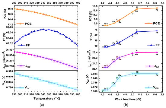
Figure 10.
Variation of PCE, FF, VOC, and JSC as a function of (a) operating temperature and (b) back metal contact work function.
The working function of the metal back contact can be crucial in improving or reducing the performance of a PSC. In mixed-halide PSCs, different materials could be used as back metal contacts. Some of the materials used as metal contacts in the simulation were as follows: silver (Ag = 4.26 eV), aluminium (Al = 4.28 eV), titanium (Ti = 4.33 eV), iron (Fe = 4.5 eV), chromium (Cr = 4.6 eV), copper (Cu = 4.65 eV), carbon (C = 5.0 eV), gold (Au = 5.1 eV), nickel (Ni = 5.12 eV), and platinum (Pt = 5.65 eV) [34,53].
Figure 10b shows the PCE, FF, JSC, and VOC as a function of the work function of various materials used as back contacts. In the Figure 10b, as the work function of the contact increased, the values of PCE, FF, JSC, and VOC also increased. According to the literature, a higher work function of the metal contact increases the built-in voltage (Vbi) and consequently improves the efficiency. However, a reduced work function value corresponds to diminished efficiency, as the electric field in proximity to the HTL/metal interface becomes negative. This is due to the propensity of holes to migrate toward the electrode [54]. In this simulation analysis, the highest PCE obtained for the mixed halide PSC was achieved with a work function of 5.1 eV, 5.12 eV, and 5.65 eV, corresponding to Au, Ni, and Pt, respectively. The objective of this study was to use gold as the back metal contact because it allows for higher efficiencies and is more stable material. Conversely, nickel emerged as a cost-effective alternative, exhibiting a lower cost but compromised stability in PSC fabrication. Platinum is another viable option; however, its cost is significantly higher [53].
3.9. J–V Characteristic Curve, EQE, and Energy Band Diagram
This section analyses the J–V characteristic curve, external quantum efficiency (EQE), and energy band diagram comparing the non-optimized and optimized mixed-halide perovskite solar cells (PSCs) simulated in SCAPS-1D. The initial mixed-halide PSC with the FTO/TiO2/CH3NH3PbI3−xClx/Spiro-OMeTAD/Au structure exhibited output parameters of VOC = 0.933 V, JSC = 26.36 mA/cm2, FF = 67.75%, and PCE = 16.67%. In contrast, after optimization, the same structure achieved enhanced performance with VOC = 1.179 V, JSC = 27.26 mA/cm2, FF = 81.03%, and PCE = 26.06%, as illustrated in Figure 11a. The simulation of the final mixed-halide PSC was conducted by incorporating the optimal parameters derived from the previous simulations. The optimized device exhibited an efficiency 9.4% higher than the initial device, demonstrating that the perovskite thickness, perovskite defects, TiO2/CH3NH3PbI3−xClx interface defects, and work function were the primary factors contributing to the performance improvement of the Cl-based PSC.
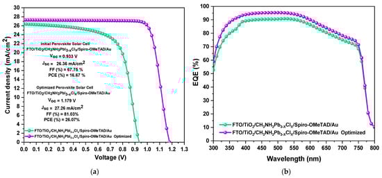
Figure 11.
(a) J–V characteristic curve and (b) EQE curve of the non-optimized mixed-halide PSC vs. the op-timized mixed-halide PSC.
Then, we obtained the external quantum efficiency (EQE) plot for both devices, as illustrated in Figure 11b. The EQE is the ratio between the total extracted charge carries in the PSC and the total incident photons. For this analysis, the EQE of both devices was simulated over a wavelength range of 300 to 800 nm. It can be observed (Figure 11b) that the non-optimized PSC exhibits an average EQE of 89% within the 380–600 nm wavelength range. On the other hand, the optimized PSC shows an average EQE of 94% within the 380–600 nm range, after which the EQE tends to decrease at longer wavelengths. Therefore, the increase in EQE is due to the incorporation of optimal parameters in the simulation, which enhances charge carrier extraction in the device.
Subsequently, Figure 12a,b show the simulated energy band diagrams of the initial mixed-halide PSC and the optimized mixed-halide PSC. In the energy band diagram of the optimized PSC, a splitting of the valence band and conduction band is observed, and changes in the thicknesses of the layers (Perovskite, ETL, and HTL) are observed due to optimization. Furthermore, the diagram illustrates that the energy band gaps of both the TiO2 and Spiro-OMeTAD layers are higher than that of the perovskite layer (CH3NH3PbI3−xClx), leading to effective energy level alignment. This alignment enhances the transport of electrons and holes generated within the perovskite layer while blocking the movement of opposite charges. Consequently, this also enables maximum photon transmission into the perovskite layer, generating more current, improving the FF, and enhancing the PCE.
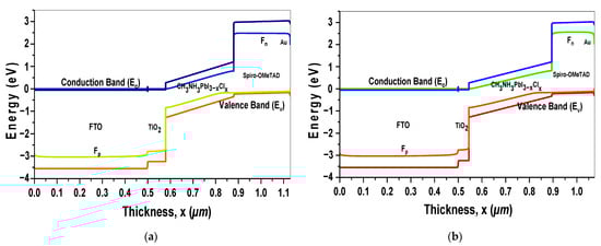
Figure 12.
(a) Energy band diagram of the non-optimized mixed-halide PSC and (b) the energy band dia-gram of the optimized mixed-halide PSC.
3.10. Comparative Study Between the Experiment and Simulation
Table 3 presents a comparative analysis of the analogous mixed-halide PSC structures reported. This table includes both experimental reports and simulation studies. These structures are selected because they are like the structure proposed in this work. Compared to experimental reports, our optimized simulation proposal exhibits significantly superior performance.
Table 3.
Experimental and simulated comparison of mixed-halide PSC structures.
4. Conclusions
In this analysis, we utilized the SCAPS-1D software to simulate and numerically optimize a mixed-halide perovskite solar cell with the structure FTO/TiO2/CH3NH3PbI3−xClx/Spiro-OMeTAD/Au. In addition, the experimentally obtained absorption coefficient of the perovskite layer was introduced into the simulator. Initially, the optimal thickness for the perovskite layer was determined to be 350 nm, while the optimal thicknesses for the ETL and HTL layers were 45 nm and 180 nm, respectively. Subsequently, the optimal defect densities for the perovskite layer and interfaces were 1014 cm−3 and 1013 cm−2, respectively. Finally, the optimal values for series resistance, shunt resistance, operating temperature, and work function of the metallic contact (gold) were 1 Ω·cm2, 5000 Ω·cm2, 300 K, and 5.1 eV, respectively. The simulation of the initial device produced performance parameters of PCE = 16.67%, FF = 67.75%, JSC = 26.36 mA/cm2, and VOC = 0.933 V. In contrast, the optimized simulation yielded improved performance parameters of PCE = 26.07%, FF = 81.03%, JSC = 27.26 mA/cm2, and VOC = 1.179 V. The analysis indicates that the primary factors contributing to the enhancement of performance are perovskite thickness, perovskite defects, ETL/perovskite interface defects, and back metal contact work function. A comparison of J–V characteristic curves between the initial and optimized devices revealed a voltage increase of 0.246 V, a rise in current density of 0.9 mA/cm2, and a 9.4% enhancement in efficiency. Regarding EQE, an increase of 5% was observed in the wavelength range of 380 to 600 for the optimized device compared to the non-optimized device. Ultimately, this study could be valuable for the fabrication of mixed-halide perovskite solar cells with a conventional architecture.
Author Contributions
Conceptualization, J.C.L. and J.A.L.L.; methodology, E.P.T.; software, E.P.T. and A.C.P.R.; validation, J.C.L., J.A.L.L., and J.Á.D.H.d.l.L.; formal analysis, E.P.T. and J.C.L.; investigation, J.Á.D.H.d.l.L. and K.M.L.; resources, J.F.-M. and A.C.P.R.; data curation, Z.J.H.S.; writing—original draft preparation, E.P.T.; writing—review and editing, E.P.T. and J.A.L.L.; visualization, J.A.L.L. and J.F.-M.; supervision, J.Á.D.H.d.l.L.; project administration, J.A.L.L. and K.M.L.; and funding acquisition, J.C.L. and J.A.L.L. All authors have read and agreed to the published version of the manuscript.
Funding
This research received no external funding.
Institutional Review Board Statement
Not applicable.
Informed Consent Statement
Not applicable.
Data Availability Statement
The original contributions presented in this study are included in the article. Further inquiries can be directed to the corresponding author.
Acknowledgments
Ezequiel Paz is grateful for the scholarship CONACYT #712701. The authors acknowledge CIDS-BUAP.
Conflicts of Interest
The authors declare no conflicts of interest.
References
- Sharif, R.; Khalid, A.; Waqas, S.; Rehman, A.; Ghulam, H.; Husnain, H.; Mahmood, K.; Afzalc, S.; Saleem, F. A comprehensive review of the current progresses and material advances in perovskite solar cells. Nanoscale Adv. 2023, 5, 3803–3833. [Google Scholar] [CrossRef] [PubMed]
- Noman, M.; Khan, Z.; Jan, S.T. A comprehensive review on the advancements and challenges in perovskite solar cell technology. RSC Adv. 2024, 14, 5085–5131. [Google Scholar] [CrossRef] [PubMed]
- Zhang, P.; Li, M.; Chen, W.C. A Perspective on Perovskite Solar Cells: Emergence, Progress, and Commercialization. Front. Chem. 2022, 10, 802890. [Google Scholar] [CrossRef]
- Diouf, B.; Muley, A.; Pode, R. Issues, Challenges, and Future Perspectives of Perovskites for Energy Conversion Applications. Energies 2023, 16, 6498. [Google Scholar] [CrossRef]
- Euvrard, J.; Yan, Y.; Mitzi, D.B. Electrical doping in halide perovskites. Nat. Rev. Mater. 2021, 6, 531–549. [Google Scholar] [CrossRef]
- Yin, Z.; Lu, B.; Chen, Y.; Guo, C. Advances of Commercial and Biological Materials for Electron Transport Layers in Biological Applications. Front. Bioeng. Biotechnol. 2022, 10, 900269. [Google Scholar] [CrossRef]
- Mehdi, H.; Mhamdi, A.; Bouazizi, A. Effect of perovskite precursor ratios and solvents volume on the efficiency of MAPbI3−xClx mixed halide perovskite solar cells. Mater. Sci. Semicond. Process. 2019, 109, 104915. [Google Scholar] [CrossRef]
- Lian, Z.; Yan, Q.; Gao, T.; Ding, J.; Lv, Q.; Ning, C.; Li, Q.; Sun, J. Perovskite CH3NH3PbI3(Cl) Single Crystals: Rapid Solution Growth, Unparalleled Crystalline Quality, and Low Trap Density toward 108 cm−3. J. Am. Chem. Soc. 2016, 138, 9409–9412. [Google Scholar] [CrossRef]
- Chae, J.; Dong, Q.; Huang, J.; Centrone, A. Chloride Incorporation Process in CH3NH3PbI3−xClx Perovskites via Nanoscale Bandgap Maps. Nano Lett. 2019, 15, 8114–8121. [Google Scholar] [CrossRef]
- Burgelman, M.; Nollet, P.; Degrave, S. Modelling polycrystalline semiconductor solar cells. Thin Solid Films 2000, 361, 527–532. [Google Scholar] [CrossRef]
- Nakka, L.; Cheng, Y.; Aberle, A.G.; Lin, F. Analytical review of spiro-OMeTAD hole transport materials: Paths toward stable and efficient perovskite solar cells. Adv. Energy Sustain. Res. 2022, 3, 2200045. [Google Scholar] [CrossRef]
- Dahiya, H.; Suthar, R.; Khandelwal, K.; Karak, S.; Sharma, G.D. Recent advances in organic and inorganic hole and electron transport layers for organic solar cells: Basic concept and device performance. ACS Appl. Electron. Mater. 2022, 4, 5119–5143. [Google Scholar] [CrossRef]
- Fatima, Q.; Haidry, A.A.; Zhang, H.; El Jery, A.; Aldrdery, M. A critical review on advancement and challenges in using TiO2 as electron transport layer for perovskite solar cell. Mater. Today Sustain. 2024, 27, 100857. [Google Scholar] [CrossRef]
- Afre, R.A.; Pugliese, D. Perovskite Solar Cells: A Review of the Latest Advances in Materials, Fabrication Techniques, and Stability Enhancement Strategies. Micromachines 2024, 15, 192. [Google Scholar] [CrossRef] [PubMed]
- Burgelman, M.; Decock, M.K.; Niemegeers, A.; Verschraegen, J.; Degrave, S. SCAPS-1D Manual; University of Gent: Gent, Belgium, 2021; p. 155. [Google Scholar]
- Burgelman, M.; Decock, K.; Kheli, S.; Abass, A. Advanced electrical simulation of thin film solar cells. Thin Solid Films 2013, 535, 296–301. [Google Scholar] [CrossRef]
- Verschraegen, J.; Burgelman, M. Numerical modeling of intra-band tunneling for heterojunction solar cells in scaps. Thin Solid Films 2007, 515, 6276–6279. [Google Scholar] [CrossRef]
- Abdelaziz, S.; Zekry, A.; Shaker, A.; Abouelatta, M. Investigating the performance of formamidinium tin-based perovskite solar cell by SCAPS device simulation. Opt. Mater. 2020, 101, 109738. [Google Scholar] [CrossRef]
- Alipour, H.; Ghadimi, A. Optimization of lead-free perovskite solar cells in normal-structure with WO3 and water-free PEDOT: PSS composite for hole transport layer by SCAPS-1D simulation. Opt. Mater. 2021, 120, 111432. [Google Scholar] [CrossRef]
- Fujiwara, H.; Collins, R.W. Spectroscopic Ellipsometry for Photovoltaics; Springer: Cham, Switzerland, 2018; pp. 519–520. [Google Scholar] [CrossRef]
- Rai, S.; Pandey, B.K.; Dwivedi, D.K. Device simulation of low cost HTM free perovskite solar cell based on TiO2 electron transport layer. AIP Conf. Proc. 2020, 2220, 140022. [Google Scholar] [CrossRef]
- Sahoo, A.; Mohanty, I.; Mangal, S. Effect of acceptor density, thickness and temperature on device performance for tin-based perovskite solar cell. Mater. Today Proc. 2022, 62, 6210–6215. [Google Scholar] [CrossRef]
- Stanić, D.; Kojić, V.; Cižmar, T.; Juraić, K.; Bagladi, L.; Mangalam, J.; Rath, T.; Gajović, A. Simulating the performance of a formamidinium based mixed cation lead halide perovskite solar cell. Materials 2021, 14, 6341. [Google Scholar] [CrossRef] [PubMed]
- Isoe, W.; Mageto, M.; Maghanga, C.; Mwamburi, M.; Odari, V.; Awino, C. Thickness Dependence of Window Layer on CH3NH3PbI3−xClx Perovskite Solar Cell. Int. J. Photoenergy 2020, 2020, 8877744. [Google Scholar] [CrossRef]
- Ayad, M.; Fathi, M.; Mellit, A. Study and performance analysis of Perovskite solar cell structure based on organic and inorganic thin films. Optik 2021, 233, 166619. [Google Scholar] [CrossRef]
- Shukla, N.; Prajapati, D.; Tiwari, S. Investigation on Design and Device Modeling of High Performance CH3NH3PbI3−xClx Perovskite Solar Cells. J. Ravishankar Univ. 2021, 34, 58–63. [Google Scholar] [CrossRef]
- Ahamed, T.; Rahaman, I.; Karmakar, S.; Halim, M.A.; Sarkar, P.K. Thickness optimization and the effect of different hole transport materials on methylammonium tin iodide (CH3NH3SnI3)-based perovskite solar cell. Emergent Mater. 2023, 6, 175–183. [Google Scholar] [CrossRef]
- Karthick, S.; Velumani, S.; Bouclé, J. Experimental and SCAPS simulated formamidinium perovskite solar cells: A comparison of device performance. Sol. Energy 2020, 205, 349–357. [Google Scholar] [CrossRef]
- Du, H.J.; Wang, W.C.; Zhu, J.Z. Device simulation of lead-free CH3NH3SnI3 perovskite solar cells with high efficiency. Chin. Phys. B 2016, 25, 108802. [Google Scholar] [CrossRef]
- Basyoni, M.S.S.; Salah, M.M.; Mousa, M.; Shaker, A.; Zekry, A.; Abouelatta, M. On the Investigation of Interface Defects of Solar Cells: Lead-Based vs Lead-Free Perovskite. IEEE Access. 2021, 9, 130221–130232. [Google Scholar] [CrossRef]
- Shubham; Raghvendra; Pathak, C.; Pandey, S.K. Design, Performance, and Defect Density Analysis of Efficient Eco-Friendly Perovskite Solar Cell. IEEE Trans. Electron. Devices 2020, 67, 2837–2843. [Google Scholar] [CrossRef]
- Abdy, H.; Aletayeb, A.; Kolahdouz, M.; Soleimani, E.A. Investigation of metal-nickel oxide contacts used for perovskite solar cell. AIP Adv. 2019, 9, 015216. [Google Scholar] [CrossRef]
- Wang, J.; Li, J.; Zhou, Y.; Yu, C.; Hua, Y.; Yu, Y.; Li, R.; Lin, X.; Chen, R.; Wu, H.; et al. Tuning an Electrode Work Function Using Organometallic Complexes in Inverted Perovskite Solar Cells. J. Am. Chem. Soc. 2021, 143, 7759–7768. [Google Scholar] [CrossRef] [PubMed]
- Behrouznejad, F.; Shahbazi, S.; Taghavinia, N.; Wu, H.P.; Wei-Guang, E. A study on utilizing different metals as the back contact of CH3NH3PbI3 perovskite solar cells. J. Mater. Chem. A 2016, 4, 13488–13498. [Google Scholar] [CrossRef]
- Ritu; Gagandeep; Kumar, R.; Chand, F. Numerical simulation of a mixed-halide perovskite solar cell using doping gradient. J. Comput. Electron. 2023, 22, 1532–1540. [Google Scholar] [CrossRef]
- Singh, P.; Ravindra, N.M. Temperature dependence of solar cell performance—An analysis. Sol. Energy Mater. Sol. Cells 2012, 101, 36–45. [Google Scholar] [CrossRef]
- Sun, S.; Buonassisi, T.; Correa-Baena, J.P. State-of-the-Art Electron-Selective Contacts in Perovskite Solar Cells. Adv. Mater. Interfaces 2018, 5, 1–9. [Google Scholar] [CrossRef]
- Baig, F.; Khattak, Y.H.; Shuja, A.; Riaz, K.; Soucase, M.B. Performance investigation of Sb2Se3 based solar cell by device optimization, band offset engineering and Hole Transport Layer in SCAPS-1D. Curr. Appl. Phys. 2020, 20, 973–981. [Google Scholar] [CrossRef]
- Kim, G.W.; Choi, H.; Kim, M.; Lee, J.; Sung, Y.S.; Park, T. Hole Transport Materials in Conventional Structural (n–i–p) Perovskite Solar Cells: From Past to the Future. Adv. Energy Mater. 2020, 10, 1–30. [Google Scholar] [CrossRef]
- Rombach, F.M.; Haque, S.A.; Macdonald, T. Lessons learned from spiro-OMeTAD and PTAA in perovskite solar cells. Energy Environ. Sci. 2021, 14, 5161–5190. [Google Scholar] [CrossRef]
- Jamal, M.S.; Shahahmadi, S.A.; Wadia, M.A.A.; Chelvanathan, P.; Asim, N.; Misran, H.; Hossain, M.I.; Ami, N.; Sopian, K.; Akhtaruzzaman, M. Effect of Defect Density and Energy Level Mismatch on the Performance of Perovskite Solar Cells by Numerical Simulation. Optik 2019, 182, 1204–1210. [Google Scholar] [CrossRef]
- Ouslimane, T.; Et-taya, L.; Elmaimouni, L.; Benami, A. Impact of absorber layer thickness, defect density, and operating temperature on the performance of MAPbI3 solar cells based on ZnO electron transporting material. Heliyon 2021, 7, e06379. [Google Scholar] [CrossRef]
- Paz-Totolhua, E.; Carrillo-López, J.; Benítez-Lara, A.; Monfil-Leyva, K.; Piñón-Reyes, A.C.; Flores-Méndez, J.; Luna-López, J.A. Numerical Simulation of an Inverted Perovskite Solar Cell Using a SiOx Layer as Down-Conversion Energy Material to Improve Efficiency and Stability. Materials 2023, 16, 7445. [Google Scholar] [CrossRef] [PubMed]
- Shockley, W.; Read, W.T. Statistics of the Recombinations of Holes and Electrons. Phys. Rev. 1952, 87, 835–842. [Google Scholar] [CrossRef]
- Gan, Y.; Zhao, D.; Qin, B.; Bi, X.; Liu, Y.; Ning, W.; Yang, R.; Jiang, Q. Numerical Simulation of High-Performance CsPbI3/FAPbI3 Heterojunction Perovskite Solar Cells. Energies 2022, 15, 7301. [Google Scholar] [CrossRef]
- Haque, M.M.; Mahjabin, S.; Khan, S.; Hossain, M.I.; Muhammad, G.; Shahiduzzaman, M.; Sopian, K.; Akhtaruzzaman, M. Study on the interface defects of eco-friendly perovskite solar cells. Sol. Energy 2022, 247, 96–108. [Google Scholar] [CrossRef]
- Rai, S.; Pandey, B.K.; Dwivedi, D.K. Modeling of highly efficient and low cost CH3NH3Pb(I1−xClx)3 based perovskite solar cell by numerical simulation. Opt. Mater. 2019, 100, 109631. [Google Scholar] [CrossRef]
- Głowienka, D.; Zhang, D.; Di-Giacomo, F.; Najafi, M.; Veenstra, S.; Szmytkowski, J.; Galagan, Y. Role of surface recombination in perovskite solar cells at the interface of HTL/CH3NH3PbI3. Nano Energy 2020, 67, 104186. [Google Scholar] [CrossRef]
- Porwal, S.; Paul, M.; Dixit, H.; Mishra, S.; Singh, T. Investigation of Defects in Cs2SnI6-Based Double Perovskite Solar Cells Via SCAPS-1D. Adv. Theory Simul. 2022, 5, 1–9. [Google Scholar] [CrossRef]
- Yan, X.; Wang, W.; Yang, X.; Yi, W.; Wang, Y.; Li, H.; Gu, W.; Sheng, C. Origin of thermal instability of CH3NH3PbI3−xClx films for photovoltaic devices. Mater. Lett. 2016, 176, 114–117. [Google Scholar] [CrossRef]
- Zandi, S.; Saxena, P.; Gorji, N.E. Numerical simulation of heat distribution in RGO-contacted perovskite solar cells using COMSOL. Sol. Energy 2019, 197, 105–110. [Google Scholar] [CrossRef]
- Devi, N.; Parrey, K.A.; Aziz, A.; Datta, S. Numerical simulations of perovskite thin-film solar cells using a CdS hole blocking layer. J. Vac. Sci. Technol. B 2018, 36, 5026163. [Google Scholar] [CrossRef]
- Shyma, A.P.; Sellappan, R. Computational Probing of Tin-Based Lead-Free Perovskite Solar Cells: Effects of Absorber Parameters and Various. Materials 2022, 15, 7859. [Google Scholar] [CrossRef]
- Jäger, T.; Romanyuk, E.Y.; Bissig, B.; Pianezzi, F.; Nishiwaki, S.; Reinhard, P.; Steinhauser, J.; Schwenk, J.; Tiwari, N.A. Improved open-circuit voltage in Cu(In,Ga)Se2 solar cells with high work function transparent electrodes. J. Appl. Phys. 2015, 117, 225303. [Google Scholar] [CrossRef]
- Wojciechowski, K.; Saliba, M.; Leijtens, T.; Abate, A.; Snaith, H.J. Sub-150 °C processed meso-superstructured perovskite solar cells with enhanced efficiency. Energy Environ. Sci. 2014, 7, 1142–1147. [Google Scholar] [CrossRef]
- Liu, Z.; Chen, Q.; Hong, Z.; Zhou, H.; Xu, X.; De-Marco, N.; Sun, P.; Zhao, Z.; Cheng, Y.B.; Yang, Y. Low-Temperature TiOx Compact Layer for Planar Heterojunction Perovskite Solar Cells. ACS Appl. Mater. Interfaces 2016, 8, 11076–11083. [Google Scholar] [CrossRef] [PubMed]
- Chen, Q.; Zhou, H.; Fang, Y.; Stieg, A.Z.; Song, T.B.; Wang, H.H.; Xu, X.; Liu, Y.; Lu, S.; You, J.; et al. The optoelectronic role of chlorine in CH3NH3PbI3 (Cl)-based perovskite solar cells. Nat. Commun. 2015, 6, 1–9. [Google Scholar] [CrossRef]
Disclaimer/Publisher’s Note: The statements, opinions and data contained in all publications are solely those of the individual author(s) and contributor(s) and not of MDPI and/or the editor(s). MDPI and/or the editor(s) disclaim responsibility for any injury to people or property resulting from any ideas, methods, instructions or products referred to in the content. |
© 2025 by the authors. Licensee MDPI, Basel, Switzerland. This article is an open access article distributed under the terms and conditions of the Creative Commons Attribution (CC BY) license (https://creativecommons.org/licenses/by/4.0/).