Article

Phase Transition Behavior and Threshold Characteristics of GeTe Thin Films Under Single-Pulse Nanosecond Laser Irradiation

College of Electronic Science and Technology, National University of Defense Technology, Changsha 410073, China
*
Author to whom correspondence should be addressed.
Materials 2025, 18(23), 5466; https://doi.org/10.3390/ma18235466 (registering DOI)
Submission received: 25 October 2025 / Revised: 19 November 2025 / Accepted: 26 November 2025 / Published: 4 December 2025

Abstract

Realizing the full potential of optical actuation for high-speed phase-change radio-frequency (RF) switches requires a shift to single-pulse operation. This work presents a systematic investigation of reversible phase transitions in GeTe thin films induced by single 10 ns laser pulses, utilizing spatially resolved characterization techniques, including atomic force microscopy (AFM) and micro-spectroscopy. Precise laser fluence windows for crystallization (12.7–16 mJ/cm2) and amorphization (25.44–41.28 mJ/cm2) are established. A critical finding is that the amorphization process is governed by rapid thermal accumulation, which creates a direct trade-off between achieving the phase transition and avoiding detrimental surface morphology. Specifically, we observe that excessive energy leads to the formation of laser-induced ridges and ablation craters, which are identified as primary causes of device performance degradation. This study elucidates the underlying mechanism of single-pulse-induced phase transitions and provides a practical processing window and design guidelines for developing high-performance, optically actuated GeTe-based RF switches.

1. Introduction

As a chalcogenide phase-change material, GeTe exhibits pronounced contrasts in electrical resistivity and optical reflectance between its crystalline and amorphous states [1,2,3]. While traditional phase-change materials like Ge2Sb2Te5 (GST) have been predominant in the non-volatile memory landscape [3], GeTe has emerged as a superior candidate for reconfigurable radio-frequency (RF) devices [4,5,6]. Its advantages include a higher crystallization temperature, which ensures enhanced thermal stability, an exceptionally high electrical resistivity contrast (>106) crucial for a high ON/OFF ratio, and superior hole mobility that benefits the ON-state insertion loss [7]. These characteristics are particularly desirable for RF switches, where signal integrity and power handling are paramount.
The actuation method for these phase-change devices is equally crucial. Laser processing has gained significant industrial relevance as a powerful material modification tool, offering unparalleled advantages in non-contact operation, spatial precision, energy efficiency, and outstanding process repeatability [8,9]. For RF systems, optical actuation presents a compelling alternative to electrical signaling by eliminating the need for integrated electrodes, thereby mitigating parasitic capacitance and enabling more flexible device architectures [10].
The fundamental kinetics of GeTe support rapid phase transitions. Extensive research has confirmed that crystallization and amorphization can be achieved on the nanosecond scale using laser pulses [11,12,13,14,15]. For instance, studies have shown that the phase transition can be completed within tens of nanoseconds [11,15]. However, when translating this fundamental speed into functional RF switches, the state of the art in optical actuation has yet to fully capitalize on it. Demonstrations, such as the work by Charlet et al. utilizing laser pulses with durations of hundreds of nanoseconds to microseconds, result in switching speeds comparable to electrical switches [16], thus failing to exploit the inherent speed advantage of photonic control [10,17,18].
This performance gap is further widened by the research focus within the GeTe community. Driven largely by the demands of multi-level memory applications, significant research efforts have been directed towards understanding and exploiting multi-pulse and gradual phase transition mechanisms [19,20,21,22,23,24], with single-pulse switching receiving considerably less attention. This prevailing trend, however, is misaligned with the operational paradigm of a high-speed RF switch. Unlike memory that may benefit from multi-level programming, an RF switch is a binary device requiring a rapid and definitive phase transition. A single-pulse paradigm is, therefore, not merely an option but a necessity for achieving ultimate switching speed, operational simplicity, and robustness. Our work addresses this critical gap by focusing on the phase transition induced by a single ~10-nanosecond laser pulse. We posit that by drastically reducing the pulse duration from the microsecond to the nanosecond regime, we can unlock the potential for switching speeds orders of magnitude faster than the current optically actuated state of the art. The investigation into the fundamental single-pulse phase control at this timescale, and its correlation with the resulting phase states and morphology, constitutes the key novelty of our study.
In this study, we systematically investigate the effects of varying fluence from a single 532 nm nanosecond laser pulse on the crystallization and amorphization processes of GeTe thin films. Using a focused Gaussian beam and characterization techniques including reflectance monitoring and AFM, we explore the mechanisms underlying these ultrafast laser-induced phase transitions. Our goal is to identify the precise laser fluence windows for controlled phase transitions and to understand the concomitant morphological changes. Based on these findings, we discuss potential strategies to mitigate ablation and improve the quality of phase transitions, paving the way for the development of future high-speed, optically actuated GeTe-based RF switches.

2. Materials and Methods

2.1. Experimental Setup

A 150 nm thick GeTe thin film (Zhongnuo New Material, Beijing, China) was deposited by magnetron sputtering (60 W, 0.4 Pa) on a 300 nm SiO2 underlayer, which serves as an effective thermal insulation layer. The selection and thickness of this insulation layer are of paramount importance for controlling the thermal dynamics during the phase transition process. Prior to laser irradiation, the samples underwent a standardized cleaning procedure to remove surface contaminants: sequential ultrasonication in acetone, ethanol, and deionized water (5 min each), followed by drying under a gentle nitrogen stream. A schematic diagram of the experimental setup and a corresponding photograph are shown in Figure 1a,b, respectively. The irradiation source was a 532 nm pulsed laser (Guangzhi Technology Co., Ltd, Wuhan, China), focused to a Gaussian spot with a D4σ beam diameter of approximately 50 μm. The samples were mounted on a computer-controlled XY translation stage, and their position was monitored in real-time using a charge-coupled device (CCD) camera. Dedicated software (Femto Easy STAR) synchronized the laser output with the stage movement. The laser pulse energy and beam profile were characterized using a laser power meter (Thorlabs) and a beam profiler, respectively.
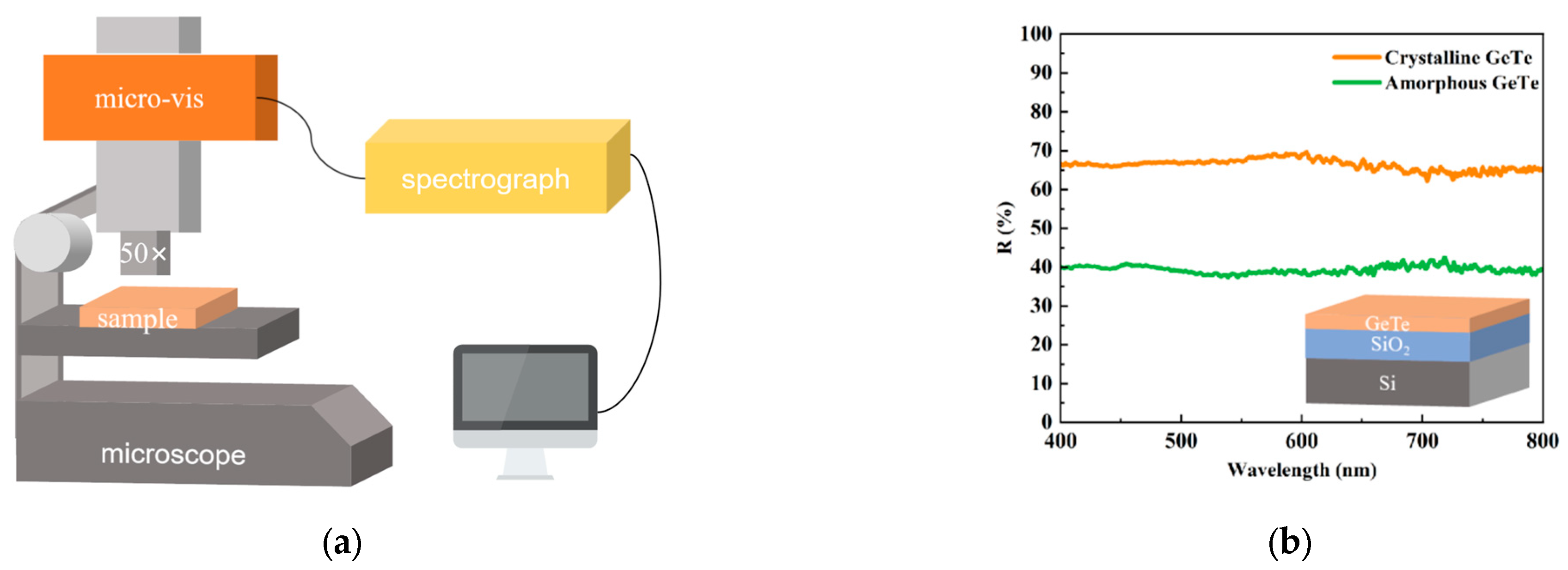
The pronounced contrast in optical reflectivity serves as a robust and well-established indicator of the crystalline-to-amorphous phase transition in GeTe and related phase-change materials [12,25]. We constructed a microscale reflectance measurement system by integrating spectroscopic modules into an optical microscopy, which can be used to quantify the reflectance of a wide spectrum ranging from 400 to 800 nm within micrometer-scale regions, as shown in Figure 2a. The measured reflectance of crystalline and amorphous GeTe is shown in Figure 2b. GeTe exhibits an obvious reflectance contrast between the two states: approximately 70% for the crystalline phase versus about 40% for the amorphous phase. Phase identification was primarily based on the characteristic reflectivity contrast between amorphous and crystalline GeTe, as measured by micro-spectroscopy.

2.2. Theoretical Analysis

Laser-induced phase transition in GeTe primarily originates from the photothermal effect. Unlike the non-thermal phase transition mechanisms potentially induced by femtosecond pulses, the phase transition driven by nanosecond pulses is primarily governed by thermal effects [26,27]. This process follows a classical thermodynamic pathway, wherein the laser heats the material above its crystallization or melting temperature, followed by a phase transition achieved through thermal conduction. Although the spatial control precision of nanosecond lasers is inferior to that of femtosecond lasers, they offer advantages in terms of lower cost and easier integration. Upon reaching the phase transition temperature threshold, GeTe undergoes a series of structural changes. When crystalline GeTe is heated above its melting point (~998 K), it transforms into a liquid state. After the pulse terminates, this molten state is rapidly quenched by the substrate at an estimated rate of ~109–1011 K/s, solidifying into an amorphous phase [28]. Conversely, when amorphous GeTe is heated above its crystallization temperature (473–673 K), its atoms gain sufficient kinetic energy to diffuse and rearrange, facilitating nucleation and subsequent crystal growth.
To model the laser-induced crystallization and amorphization processes in GeTe, we performed simulations using the COMSOL Multiphysics software (Version 6.1, Stockholm, Sweden). In this model, the laser energy incident on the material surface causes a rapid temperature increase. The resulting energy transfer is governed by thermal radiation to the surroundings, heat conduction into the material bulk, and natural convection in the adjacent air. Accordingly, an energy conversion model accounting for these phenomena can be established [29].
ρ C p T t k × T + h ( T 0 T ) + ε σ ( T 0 4 T 4 ) = Q
Here, ρ ,   C p , k , h ,   ε and σ represent the material’s density, specific heat capacity, thermal conductivity, convective heat transfer coefficient, emissivity, and the Stefan–Boltzmann constant, respectively.
The incident laser beam undergoes rapid attenuation upon penetration into GeTe, where absorption follows the Beer–Lambert law [19]. The laser power density within the phase-change film decays exponentially; I(z) represents the depth-dependent laser irradiance:
I ( z ) = 1 R × I 0 × e x p ( α z )
where I 0 is incident irradiance at the surface (z = 0), α is absorption coefficient of GeTe (cm−1), and z is depth coordinate (μm).
In the radiation beam module of the absorption medium, the light spot type is set as a Gaussian spot; the incident beam power density deposited on the thin-film surface is given by
P = ( E × S ) / τ × g ( t ) × ( 1 R )
where E is the laser fluence, S is the irradiated area, R is the surface reflectivity, and g ( t ) represents the laser temporal profile such as rectangular or Gaussian pulses.
In this specific experiment, the experimental power measured by a power meter was used to derive the single-pulse energy, ultimately yielding the deposited beam power.
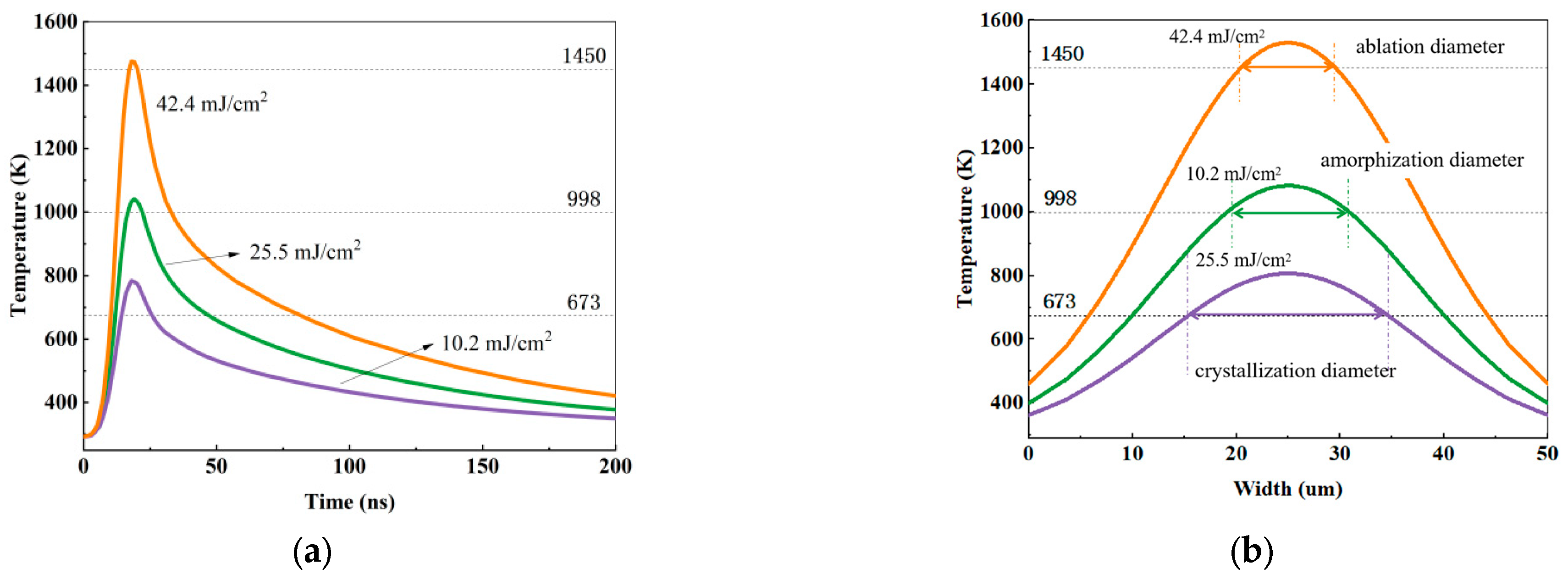
COMSOL thermal simulations of crystalline and amorphous states of GeTe under varying laser fluence levels reveal dynamic surface temperature evolution (Figure 3); the material parameters are shown in Table 1. Figure 3a demonstrates transient thermal profiles within a 10 µm surface region, where rapid heating (≤20 ns) followed by gradual cooling completes the thermal cycle within 200 ns. Horizontally dashed lines mark critical thresholds for ablation (1450 K), amorphization (998 K), and crystallization (673 K). Corresponding cross-sectional temperature distributions in Figure 3b enable quantification of the diameters of the phase-changed regions via critical isotherm propagation (e.g., 1450 K). These simulated diameters are quantitatively validated against experimental measurements in Section 3.
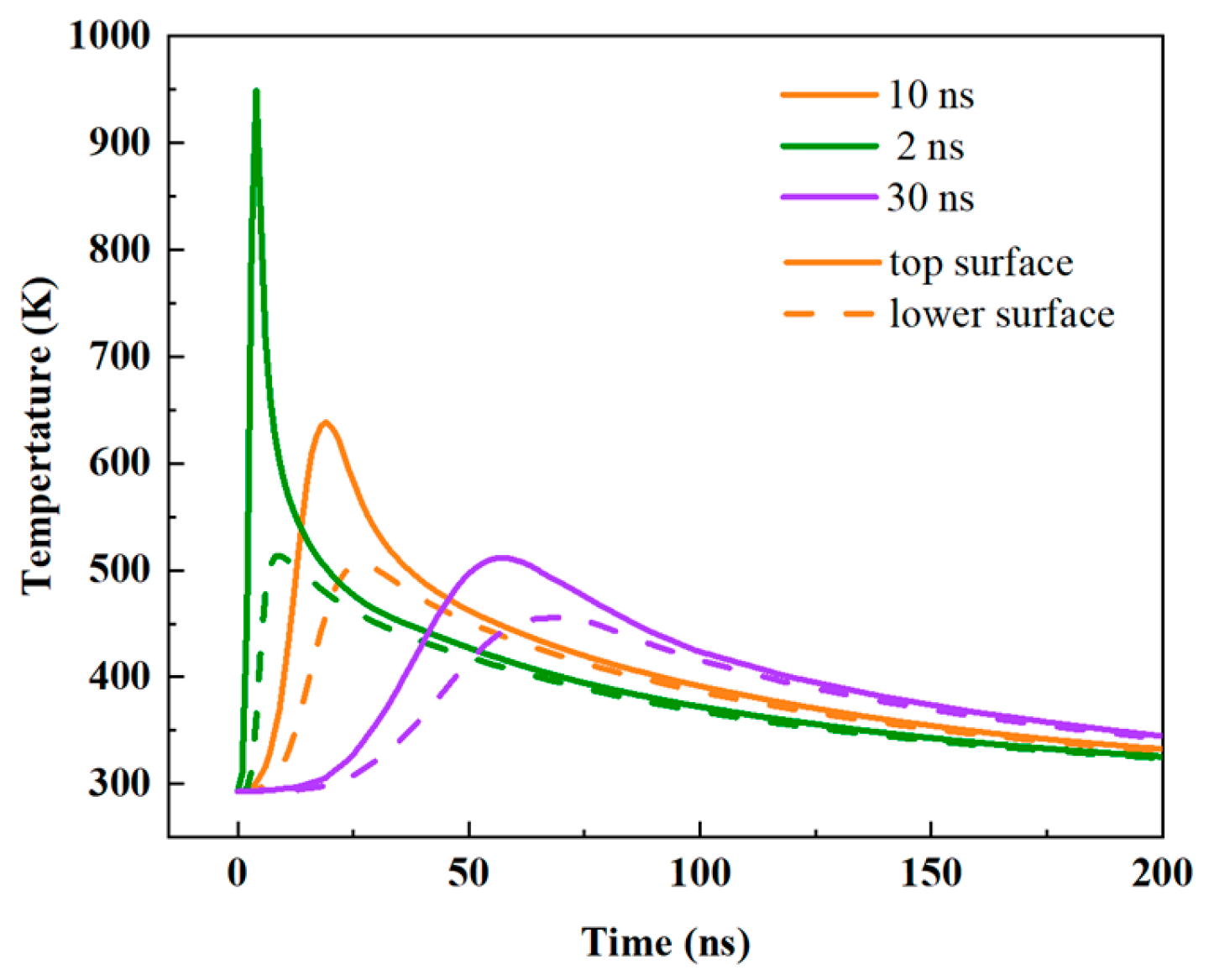
In this experiment, a laser pulse width of 10 ns was employed. The nucleation and crystalline growth processes of GeTe occur on timescales ranging from nanoseconds to tens of nanoseconds. A 10 ns laser pulse provides sufficient duration for nucleus formation and short-range atomic diffusion, facilitating the formation of uniform, high-quality crystals. Concurrently, its brevity is adequate to prevent excessive grain growth and thermal diffusion. As shown in Figure 4, at the same laser fluence, a shorter pulse width can achieve a higher peak temperature. However, this induces a greater temperature gradient across the GeTe film, leading to inferior phase transition homogeneity, a narrower process window, and more challenging control. Conversely, a 30 ns laser pulse may result in secondary crystallization due to an insufficient cooling rate. The 10 ns timescale is well-matched with the intrinsic crystallization kinetics (nucleation and growth) of GeTe, thereby contributing to high-performance reversible phase transitions.

3. Results and Discussion

3.1. Amorphization Behavior

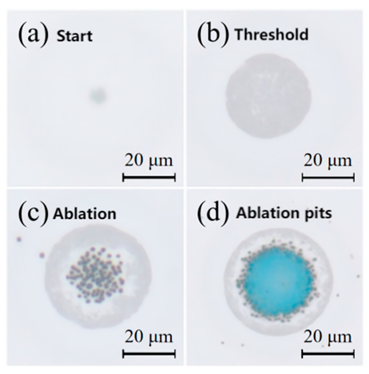
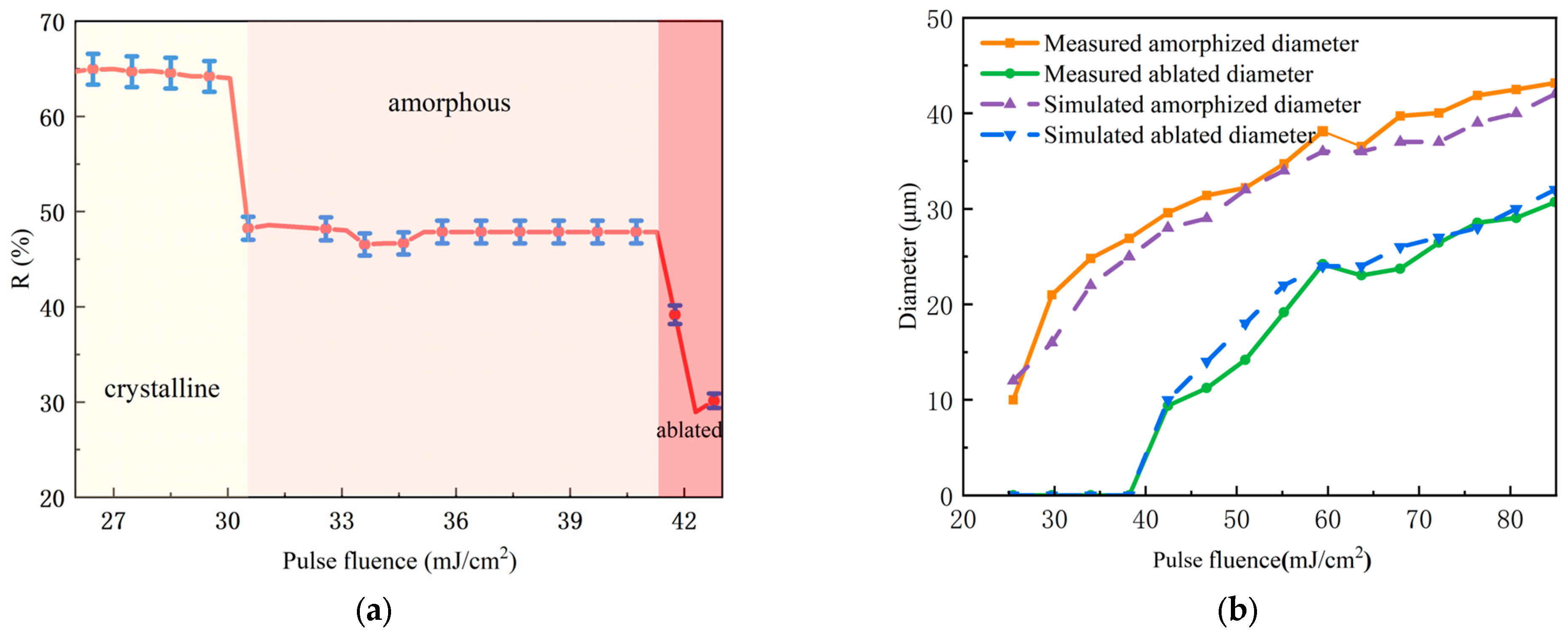
Laser irradiation induced a series of amorphized spots on the initially crystalline GeTe films. Progressive increases in laser fluence revealed four distinct stages of surface evolution, as illustrated in Figure 5. The corresponding changes in reflectance during amorphization were characterized by micro-spectroscopy (Figure 6a), which delineated the following stages:
  • Initial stage (<25.44 mJ/cm2): No significant morphological changes were observed.
  • Amorphization stage (25.44–41.28 mJ/cm2): This higher fluence range delivered enough energy to completely melt the GeTe film (temperature > 998 K). Gray circular spots emerged, indicating phase transition (Figure 5a). The diameter of amorphized regions increased with laser power, attributed to the radial threshold gradient of the Gaussian energy profile (Figure 5b). The reflectivity of the amorphized region decreased to 47% ± 2%. The simulated laser fluence threshold was verified by micro-spectroscopic measurements. The detected reflectance change occurred at a slightly lower fluence than that needed for an optically visible spot, as the spectroscopic method is more sensitive to incipient phase transitions. In the fluence of 38 mJ/cm2, the maximum ablation-free amorphized diameter reached 25 μm.
  • Ablation stage (>41.28 mJ/cm2): The spot coverage approached 50 μm, with the expansion rate decreasing as ablation initiated (Figure 5c). Further increasing the fluence causes the central temperature to exceed the ablation threshold, leading to observable ablation. The resulting surface became populated with particulates, consequently enhancing diffuse scattering and reducing the measured reflectance to around 30%. Ultimately, at the highest fluences, the blue SiO2 substrate was exposed, confirming the complete ejection of GeTe from the central region.
Based on the theoretical analysis presented in Section 2, the evolution and distribution of the surface phase transition temperature were derived. Amorphization initiates when the temperature exceeds 998 K [19], while material ablation occurs at temperatures exceeding 1450 K. Figure 6b compares these simulation results with experimental measurements, demonstrating excellent agreement between the experimentally measured curve and the finite element method (FEM) simulation results. The diameter of the amorphization region exhibits a strong dependence on laser fluence, with a marked nonlinear relationship.
AFM 2D topography characterization was conducted on amorphized and ablated regions, as illustrated in Figure 7. The AFM images were quantitatively analyzed using Gwyddion 2.58 software. The line profiles in Figure 7c,d, which were extracted along the corresponding lines in Figure 7a,b, respectively, reveal the cross-sectional height distribution of the surface structures. In Figure 7a, the amorphized area exhibits distributed small spikes surrounded by peripheral ridge structures. The Gaussian beam profile results in lower fluence at the periphery. Driven by thermal gradients and the Marangoni effect [24], the resulting surface-tension imbalance propels molten material toward cooler regions, thereby forming ridge structures. Height variations in the peripheral ridges are attributed to film preparation defects. These laser-induced protrusions, formed during high-energy pulse amorphization, degrade electrode contact performance and could emerge as critical failure factors in future device fabrication.
When laser fluence exceeds the ablation threshold of GeTe films, ablation occurs—characterized by the formation of ablation particles and pits (Figure 5c). At this time, the laser fluence is 45 mJ/cm2, and the diameter of the central ablation area is about 15 μm, which is consistent with the ablation diameter in the simulation. The central region undergoes initial disruption, generating ablation particles as shown in Figure 7b: a substantial increase in RMS roughness was observed. Central protrusions rise approximately 60 nm above the surface with subsurface depressions approximately 40 nm deep. Molten GeTe aggregates into protrusions while partially ejecting as droplets—thereby contributing to particulate formation. As laser fluence increases, peripheral regions subsequently reach melting temperatures. With further temperature increases, vaporization and material removal ensue, ultimately forming ablation pits (Figure 5d). Here, vapor recoil pressure drives molten material to expand radially outward, yielding raised rims around the pits. This ablation not only significantly increases RMS roughness but also alters GeTe composition. The irreversible material removal represents permanent film damage, ultimately leading to material failure.

3.2. Crystallization Behavior

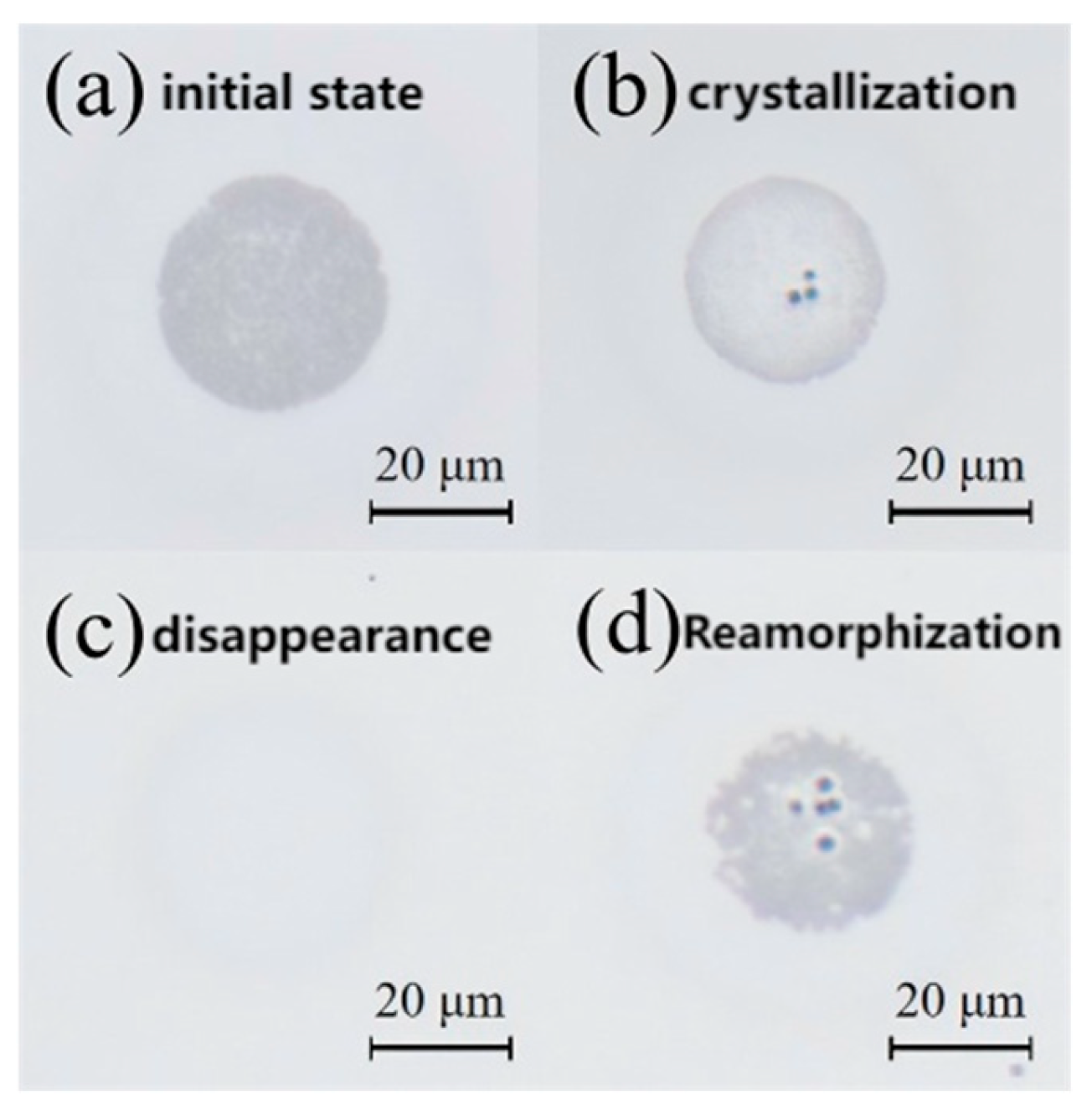
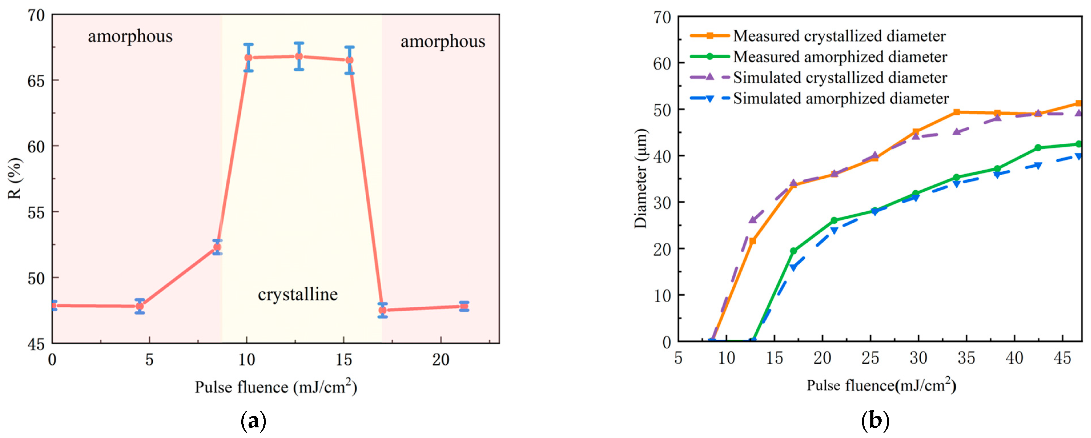
To investigate the crystallization behavior of GeTe thin films, a pulsed laser with a fluence of 38 mJ/cm2 was initially employed to irradiate the GeTe thin film, creating an amorphized region with a diameter of 25 μm. The crystallization behavior of these amorphized regions was then studied. As depicted in Figure 8, four distinct evolution stages emerge; Figure 9a demonstrates reflectance transitions: as fluence increases, surface reflectance first reaches crystalline levels then reverts to amorphous-state levels.
  • Initial state: When there is no pulse excitation or the pulse energy is lower than 8.5 mJ/cm2, the original amorphous state is maintained.
  • Crystallization (8.5–15 mJ/cm2): Within this range, the laser energy deposition is sufficient to raise the film temperature above the crystallization temperature (~673 K) but below the melting point (~998 K). When laser fluence exceeds 8.5 mJ/cm2, the degree of amorphization weakens and the reflectivity increases; when laser fluence exceeds 10.2 mJ/cm2, the amorphous spot completely disappears. At this point, the surface reflectivity of GeTe film is about 67%, which has been crystallized. This energy input provides the necessary thermal activation for atomic rearrangement, allowing for the growth of crystallized nuclei from the amorphous matrix through a solid-phase crystallization mechanism.
  • Reamorphization state (>15 mJ/cm2): Further increasing fluence causes the central region temperature to exceed the amorphous threshold, leading to reamorphization, and the reflectivity level of GeTe film returns to amorphous state.
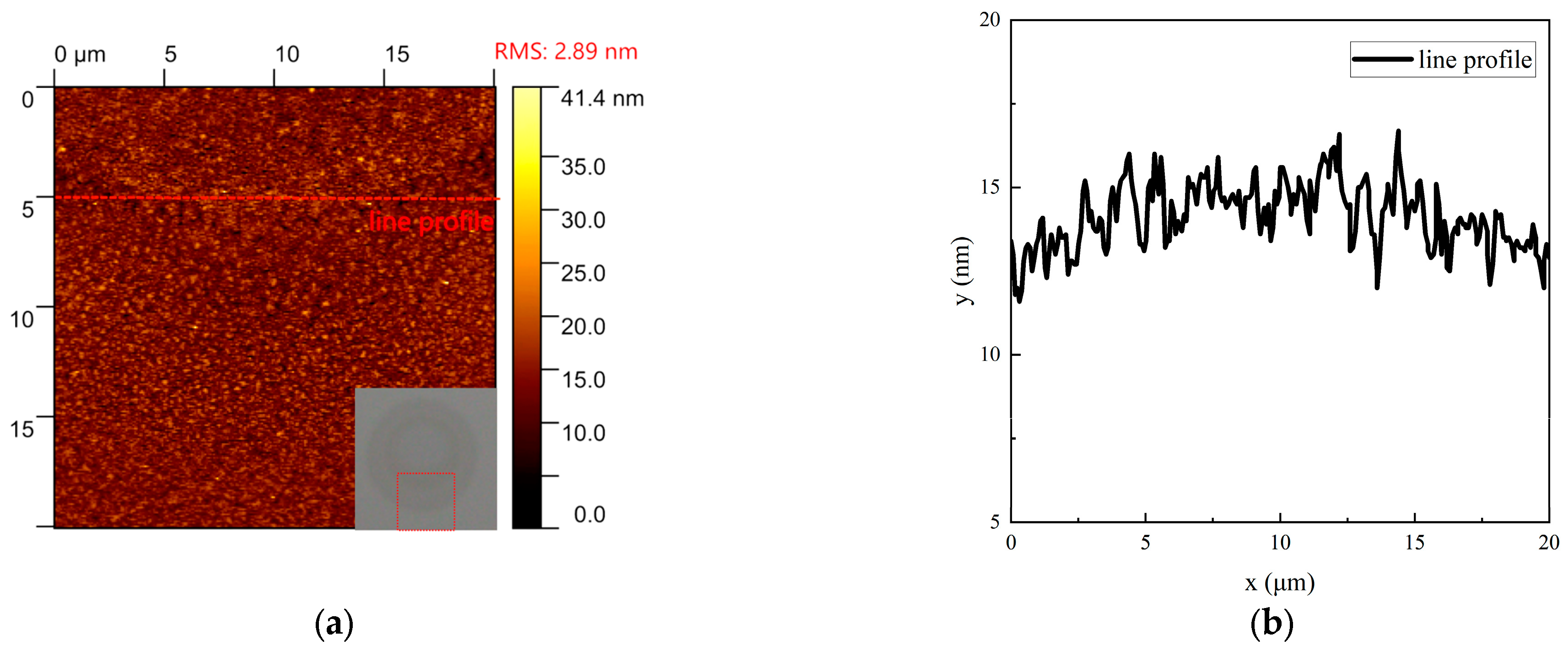
The spot diameter evolution versus laser fluence in Figure 9b shows crystalline/amorphous diameters from simulations and experiments, exhibiting trends consistent with Figure 6b. AFM analysis (Figure 10) indicates a ~5 nm surface height after recrystallization, showing collapsed morphology with reduced protrusions. Volume shrinkage during crystallization promotes inward collapse and surface planarization [16].
Cyclic phase transition was further investigated. While single-phase transition caused no damage (Figure 11), repetitive induction at identical power induced cumulative edge effects. Irreversible damage occurred during the recrystallization process. As shown in Figure 11e, ablation particles were formed after three cycles, which posed a great challenge to the cycle durability of GeTe. In order to improve the durability of GeTe, this can be mitigated by optimizing the laser beam profile (e.g., using a flat-top beam to alleviate edge effects) and by improving the film quality to reduce defect formation, thereby suppressing the development of surface spikes during laser irradiation.
In this study, we developed a multiphysics-coupled model integrating laser energy and phase transition temperature to calculate the laser energy required for GeTe thin-film phase transition under Gaussian pulse excitation, with experimental verification. Compared to the existing literature (Table 2) that predominantly employs multi-pulse excitation methods, our approach using a 532 nm laser with narrower pulse width in reference [12] achieves more efficient laser energy utilization. While the Gaussian spot configuration in this study reduces phase transition energy requirements, morphological characterization and cyclic testing demonstrate that the lower energy consumption compromises GeTe’s phase transition stability and increases failure risks.

4. Conclusions

This study demonstrates selective and reversible phase transitions in 150 nm GeTe films induced by single 10 ns Gaussian laser pulses, where non-volatile amorphization and crystallization are controlled precisely via laser fluence. The principal conclusions are summarized as follows:
  • The threshold fluences were quantitatively determined: recrystallization occurs at 8.5 mJ/cm2, while melt-quenching amorphization requires 25.4 mJ/cm2, consistent with coupled thermal–optical simulations and time-resolved reflectometry.
  • Morphological degradation—including increased roughness, nanoscale protrusions, and cyclical ablative loss—currently limits endurance. This underscores the material-level challenge in achieving high-cycle operability.
  • For the realization of reliable optically addressable phase-change devices, future efforts should concentrate on (i) optimizing GeTe stoichiometry and interfacial adhesion, (ii) developing engineered beam profiles with flat-top intensity distributions, and (iii) investigating the early stages of degradation to implement predictive failure mitigation strategies.

Author Contributions

Conceptualization, Y.L. and X.M.; methodology, Q.C.; software, Y.L.; validation, Y.L., X.M. and Y.J.; formal analysis, Y.L. and Y.J.; investigation, S.Q.; resources, Q.C.; data curation, Y.L.; writing—original draft preparation, Y.L.; writing—review and editing, S.Q., X.M. and Q.C.; visualization, Y.L.; supervision, Q.C.; project administration, Q.C., Y.Z. and Y.F.; funding acquisition, Q.C., Y.Z. and Y.F. All authors have read and agreed to the published version of the manuscript.

Funding

This research work was supported by the National Natural Science Foundation of China under Grant 61901492.

Institutional Review Board Statement

Not applicable.

Informed Consent Statement

Not applicable.

Data Availability Statement

The original contributions presented in this study are included in the article. Further inquiries can be directed to the corresponding author.

Conflicts of Interest

The authors declare no conflicts of interest.

Abbreviations

The following abbreviations are used in this manuscript:
GeTeGermanium telluride
AFMAtomic Force Microscope
CCDCharge-Coupled Device
RFRadio-Frequency
GSTGeSbTe
UVUltraviolet
FEMFinite Element Method
RMSRoot-Mean-Square Error

References

  1. Bahl, S.K.; Chopra, K.L. Amorphous versus Crystalline GeTe Films. III. Electrical Properties and Band Structure. J. Appl. Phys. 1970, 41, 2196–2212. [Google Scholar] [CrossRef]
  2. Wełnic, W.; Botti, S.; Reining, L.; Wuttig, M. Origin of the optical contrast in phase-change materials. Phys. Rev. Lett. 2007, 98, 236403. [Google Scholar] [CrossRef] [PubMed]
  3. Wuttig, M.; Bhaskaran, H.; Taubner, T. Phase-change materials for non-volatile photonic applications. Nat. Photonics 2017, 11, 465–476. [Google Scholar] [CrossRef]
  4. Chua, E.K.; Shi, L.P.; Zhao, R.; Lim, K.G.; Chong, T.C.; Schlesinger, T.E.; Bain, J.A. Low resistance, high dynamic range reconfigurable phase change switch for radio frequency applications. Appl. Phys. Lett. 2010, 97, 418–419. [Google Scholar] [CrossRef]
  5. Singh, T.; Mansour, R.R. Experimental Investigation of Performance, Reliability, and Cycle Endurance of Nonvolatile DC-67 GHz Phase-Change RF Switches. IEEE Trans. Microw. Theory Tech. 2021, 69, 4697–4710. [Google Scholar] [CrossRef]
  6. Zhang, Y.; Fowler, C.; Liang, J.; Azhar, B.; Shalaginov, M.Y.; Deckoff-Jones, S.; An, S.; Chou, J.B.; Roberts, C.M.; Liberman, V.; et al. Electrically reconfigurable non-volatile metasurface using low-loss optical phase-change material. Nat. Nanotechnol. 2021, 16, 661–666. [Google Scholar] [CrossRef]
  7. Park, J.W.; Eom, S.H.; Lee, H.; Da Silva, J.L.; Kang, Y.S.; Lee, T.Y.; Khang, Y.H. Optical Properties of Pseudobinary Gete, Ge2sb2te5, Gesb2te4, Gesb4te7, And Sb2te3 from Ellipsometry and Density Functional Theory. Phys. Rev. B 2009, 80, 115209. [Google Scholar]
  8. Gaković, B.; Petrović, S.; Siogka, C.; Milovanović, D.; Momčilović, M.; Tsibidis, G.D.; Stratakis, E. Selective Ablation and Laser-Induced Periodical Surface Structures (LIPSS) Produced on (Ni/Ti) Nano Layer Thin Film with Ultra-Short Laser Pulses. Photonics 2024, 11, 1054. [Google Scholar] [CrossRef]
  9. Laprais, C.; Zrounba, C.; Bouvier, J.; Blanchard, N.; Bugnet, M.; Gassenq, A.; Gutiérrez, Y.; Vazquez-Miranda, S.; Espinoza, S.; Thiesen, P.; et al. Reversible Single-Pulse Laser-Induced Phase Change of Sb2S3 Thin Films: Multi-Physics Modeling and Experimental Demonstrations. Adv. Opt. Mater. 2024, 12, 2401214. [Google Scholar] [CrossRef]
  10. Crunteanu, A.; Huitema, L.; Orlianges, J.C.; Guines, C.; Passerieux, D. Optical switching of GeTe phase change materials for high-frequency applications. In Proceedings of the 2017 IEEE MTT-S International Microwave Workshop Series on Advanced Materials and Processes for RF and THz Applications (IMWS-AMP), Pavia, Italy, 20–22 September 2017; IEEE: Piscataway, NJ, USA, 2017. [Google Scholar]
  11. Gawelda, W.; Siegel, J.; Afonso, C.N.; Plausinaitiene, V.; Abrutis, A.; Wiemer, C. Dynamics of laser-induced phase switching in GeTe films. J. Appl. Phys. 2011, 109, 123102. [Google Scholar] [CrossRef]
  12. Sun, X.; Thelander, E.; Lorenz, P.; Gerlach, J.W.; Decker, U.; Rauschenbach, B. Nanosecond laser-induced phase transitions in pulsed laser deposition-deposited GeTe films. J. Appl. Phys. 2014, 116, 133501. [Google Scholar] [CrossRef]
  13. Salicio, O.; Wiemer, C.; Fanciulli, M.; Gawelda, W.; Siegel, J.; Afonso, C.N.; Plausinaitiene, V.; Abrutis, A. Effect of pulsed laser irradiation on the structure of GeTe films deposited by metal organic chemical vapor deposition: A Raman spectroscopy study. J. Appl. Phys. 2009, 105, 33520–33521. [Google Scholar] [CrossRef]
  14. Sun, X.; Thelander, E.; Gerlach, J.W.; Decker, U.; Rauschenbach, B. Crystallization kinetics of GeTe phase-change thin films grown by pulsed laser deposition. J. Phys. D Appl. Phys. 2015, 48, 295304–295306. [Google Scholar] [CrossRef]
  15. Raoux, S.; Cabral, C.; Krusin-Elbaum, L.; Jordan-Sweet, J.L.; Virwani, K.; Hitzbleck, M.; Salinga, M.; Madan, A.; Pinto, T.L. Phase transitions in Ge–Sb phase change materials. J. Appl. Phys. 2009, 105, 064918. [Google Scholar] [CrossRef]
  16. Fu, S.; Gao, L.; Peng, Y.; Qu, S.; Wang, J.; Chen, H.; Liu, N.; Zhang, J. Novel four-port RF phase change switches based on GeTe thin film. J. Micromechanics Microeng. 2023, 33, 095004. [Google Scholar] [CrossRef]
  17. Ionin, V.V.; Kiselev, A.V.; Eliseev, N.N.; Mikhalevsky, V.A.; Pankov, M.A.; Lotin, A.A. Multilevel reversible laser-induced phase transitions in GeTe thin films. Appl. Phys. Lett. 2020, 117, 011901. [Google Scholar] [CrossRef]
  18. Charlet, I.; Guerber, S.; Naoui, A.; Charbonnier, B.; Dupré, C.; Lugo-Alvarez, J.; Hellion, C.; Allain, M.; Podevin, F.; Perret, E.; et al. Optical Actuation Performance of Phase-Change RF Switches. IEEE Electron. Device Lett. 2024, 45, 500–503. [Google Scholar] [CrossRef]
  19. Eliseev, N.; Kiselev, A.; Ionin, V.; Mikhalevsky, V.; Burtsev, A.; Pankov, M.; Karimov, D.; Lotin, A. Wide range optical and electrical contrast modulation by laser-induced phase transitions in GeTe thin films. Results Phys. 2020, 19, 103466. [Google Scholar] [CrossRef]
  20. Sevison, G.A.; Burrow, J.A.; Guo, H.; Sarangan, A.; Hendrickson, J.R.; Agha, I. Wavelength and power dependence on multilevel behavior of phase change materials. AIP Adv. 2021, 11, 85327. [Google Scholar] [CrossRef]
  21. Lu, H.; Thelander, E.; Gerlach, J.W.; Decker, U.; Zhu, B.; Rauschenbach, B. Single Pulse Laser-Induced Phase Transitions of PLD-Deposited Ge2Sb2Te5Films. Adv. Funct. Mater. 2013, 23, 3621–3627. [Google Scholar] [CrossRef]
  22. Wintersteller, S.; Yarema, O.; Kumaar, D.; Schenk, F.M.; Safonova, O.V.; Abdala, P.M.; Wood, V.; Yarema, M. Unravelling the amorphous structure and crystallization mechanism of GeTe phase change memory materials. Nat. Commun. 2024, 15, 1011. [Google Scholar] [CrossRef]
  23. Sun, X.; Lotnyk, A.; Ehrhardt, M.; Gerlach, J.W.; Rauschenbach, B. Realization of Multilevel States in Phase-Change Thin Films by Fast Laser Pulse Irradiation. Adv. Opt. Mater. 2017, 5, 1700169. [Google Scholar] [CrossRef]
  24. Dun, A.; Wei, J.; Gan, F. Marangoni effect induced micro/nano-patterning on Sb2Te3 phase change thin film by laser pulse. Appl. Phys. A 2011, 103, 139–147. [Google Scholar] [CrossRef]
  25. Bahl, S.K.; Chopra, K.L. Amorphous Versus Crystalline GeTe Films. II. Optical Properties. J. Appl. Phys. 1969, 40, 4940–4947. [Google Scholar] [CrossRef]
  26. Santala, M.K.; Reed, B.W.; Raoux, S.; Topuria, T.; LaGrange, T.; Campbell, G.H. Irreversible reactions studied with nanosecond transmission electron microscopy movies: Laser crystallization of phase change materials. Appl. Phys. Lett. 2013, 102, 174105. [Google Scholar] [CrossRef]
  27. Nevzorov, A.; Mikhalevsky, V.; Eliseev, N.; Kiselev, A.; Burtsev, A.; Ionin, V.; Maliutin, A.; Khmelenin, D.; Glebov, V.; Lotin, A. Two-stage conductivity switching of GST thin films induced by femtosecond laser radiation. Opt. Laser Technol. 2023, 157, 108773. [Google Scholar] [CrossRef]
  28. Bastard, A.; Bastien, J.C.; Hyot, B.; Lhostis, S.; Mompiou, F.; Bonafos, C.; Servanton, G.; Borowiak, C.; Lorut, F.; Bicais-Lepinay, N.; et al. Crystallization study of “melt quenched” amorphous GeTe by transmission electron microscopy for phase change memory applications. Appl. Phys. Lett. 2011, 99, 243103. [Google Scholar] [CrossRef]
  29. Li, Z.; Xu, J.; Zhang, D.; Shan, D.; Guo, B. Finite element simulation of temperature field in laser cleaning of TA15 titanium alloy oxide film. Sci. China Technol. Sci. 2022, 52, 318–332. [Google Scholar] [CrossRef]
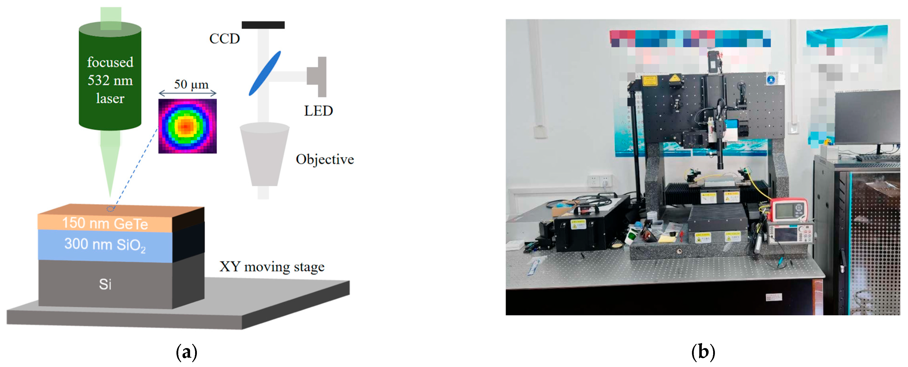
Figure 1. Scheme of the laser experimental setup: (a) schematic diagram; (b) machining platform.
Materials 18 05466 g001
Figure 2. Schematic diagram and results of reflectance measurement: (a) schematic diagram; (b) reflectivity of as-deposited GeTe and annealed crystalline GeTe.
Materials 18 05466 g002
Figure 3. Simulated temperature evolution: (a) time-resolved temperature profiles at the center (10 μm-diameter region) of the GeTe surface under three laser fluence levels; (b) cross-sectional temperature distributions across the GeTe surface at t = 20 ns for the corresponding fluence conditions.
Materials 18 05466 g003
Figure 4. Temperature variations of crystalline GeTe under different pulse widths at 30 mW laser power. The solid lines represent the top surface and the dashed lines (green and purple) represent the lower surface.
Materials 18 05466 g004
Figure 5. Amorphization phenomena of GeTe observed under the microscope: (a) initiation of amorphization; (b) expansion of the amorphized region; (c) formation of ablation particles; (d) creation of ablation pits and appearance of the blue SiO2.
Materials 18 05466 g005
Figure 6. Variations in the amorphized spot with increasing laser fluence: (a) reflectivity changes, where the red dashed line represents the reflectivity of annealed crystalline GeTe and the blue dashed line corresponds to the reflectivity of as-deposited amorphous GeTe; (b) changes in the amorphization diameter and ablation diameter, as obtained from both simulation and experimental measurements.
Materials 18 05466 g006
Figure 7. AFM images of the amorphous (38 mJ/cm2) and ablated (45 mJ/cm2) regions formed by single-pulse irradiatio: (a) amorphous state, RMS:17.7 nm; (b) ablated state, RMS:33.37 nm; (c) Roughness line profiles along the dashed lines in (a). (d) Roughness line profiles along the dashed lines in (b).
Materials 18 05466 g007
Figure 8. Single-pulse crystallization of pre-amorphized GeTe (amorphized at 38 mJ/cm2): (a) no fluence; (b) 8.5 mJ/cm2; (c) 12.7 mJ/cm2; (d) 16 mJ/cm2.
Materials 18 05466 g008
Figure 9. Variations in the crystallized region: (a) reflectivity changes under different pulse fluences; (b) changes in the diameters of the crystallized and amorphized regions with increasing pulse fluence, as obtained from both simulation and experimental measurements.
Materials 18 05466 g009
Figure 10. Recrystallization: (a) AFM images of the amorphous (38 mJ/cm2) and crystallized (10.2 mJ/cm2) regions formed by sequential single-pulse irradiation, RMS: 2.89 nm; (b) Roughness line profiles along the dashed lines in (a).
Materials 18 05466 g010
Figure 11. Phase transition states under the microscope: (a) first amorphized state; (b) first transition cycle (amorphization → crystallization); (c) second amorphized state after two amorphization and one crystallization cycles; (d) second transition cycle (two amorphization + two crystallization); (e) third transition cycle showing particulate formation (three amorphization + three crystallization).
Materials 18 05466 g011
Table 1. Material parameters.
SiO2GeTe_aGeTe_c
Cp [J/(kg·K)]730278252
Rho [kg/m3]220356005910
Thermal conductivity [W/(m·K)]1.383.083.08
Absorption coefficient [1/m]1 × 10−35.71 × 1076.64 × 107
Conductivity [S/m]00.643 × 105
Relative dielectric constant4.21818
Transition temperature [K]-473–673998
Erosion temperature--1450
Table 2. Comparison of energy thresholds for phase transition in GeTe films under different laser parameters.
DocumentGeTe ThicknessSubstrateLaser ParametersCrystallizationAmorphization
[23]75 nmSi248 nm, 20 ns, pump-probe setup26 mJ/cm2, 5 pulses112 mJ/cm2
[25]60 nmSi248 nm, 20 ns, pump-probe setup11–14 mJ/cm2 >5 pulses162–182 mJ/cm2
[12]200 nmAl2O3248 nm, 30 ns,
a KrF
excimer laser
90 mJ/cm2180 mJ/cm2
[17]100 nmSiO2532 nm, 13 ns,
Top hat
47.6 mJ/cm270 mJ/cm2
This work150 nmSiO2532 nm, 10 ns,
Gaussian
8.5–15 mJ/cm225.4 mJ/cm2
Disclaimer/Publisher’s Note: The statements, opinions and data contained in all publications are solely those of the individual author(s) and contributor(s) and not of MDPI and/or the editor(s). MDPI and/or the editor(s) disclaim responsibility for any injury to people or property resulting from any ideas, methods, instructions or products referred to in the content.