Article

Analysis of Superjunction MOSFET (CoolMOS™) Concept Limitations—Part I: Theory

Department of Semiconductor and Optoelectronic Devices, Lodz University of Technology, Aleje Politechniki 8, 93-590 Lodz, Poland
*
Author to whom correspondence should be addressed.
Materials 2025, 18(23), 5451; https://doi.org/10.3390/ma18235451 (registering DOI)
Submission received: 21 October 2025 / Revised: 29 November 2025 / Accepted: 1 December 2025 / Published: 3 December 2025
(This article belongs to the Special Issue Metal Oxide Semiconductors: Synthesis, Structure, and Applications)

Abstract

The CoolMOS™ (Infineon Technologies AG, Munich, Germany) has been considered a device that alleviates high-voltage limitations of unipolar power devices, but although the theoretical considerations seem to confirm such a possibility, this expectation has not been fulfilled until now. This paper identifies limitations of the CoolMOS™ concept. The analysis was carried out in two steps. The first step aimed at the theory of high-voltage superjunction and its implementation into a power VDMOS transistor, which resulted in the modified construction called CoolMOS™. The investigations have shown that the superjunction effect is not an inherent feature of high voltage junctions formed as a characteristic meander-like p-n junction. Such a junction starts to work in SuperJunction Mode (SJM) just when the electric field strength reaches the magnitude of the threshold electric field Eth. Also, other theoretical constraints concerning the SJ diode and CoolMOS™ design have been presented. The second step aimed at the physical and technological limitations that have been identified, taking advantage of numerical investigations for CoolMOS™ structures developed on the basis of a typical VDMOS one.

1. Introduction

The concept of the CoolMOS™ transistor is based on the conventional MOSFET principle that has been supplemented by the superjunction idea used for the reconstruction of the high voltage junction [1,2]. The main disadvantage of the conventional VDMOS (Vertical Double Diffusion MOS), limiting its high voltage applications, consists of the presence of a low-doped n-layer. Its large width is necessary to meet high blocking voltages, but it leads to an unacceptably high forward voltage. The CoolMOS™ design was created to solve this problem by reconstructing the high voltage junction. Now, its cell, shown in Figure 1, consists of one central n-doped column surrounded by two p-doped ones characterized by the same doping level, and the plane of the high voltage junction is partially vertical instead of being horizontal only.
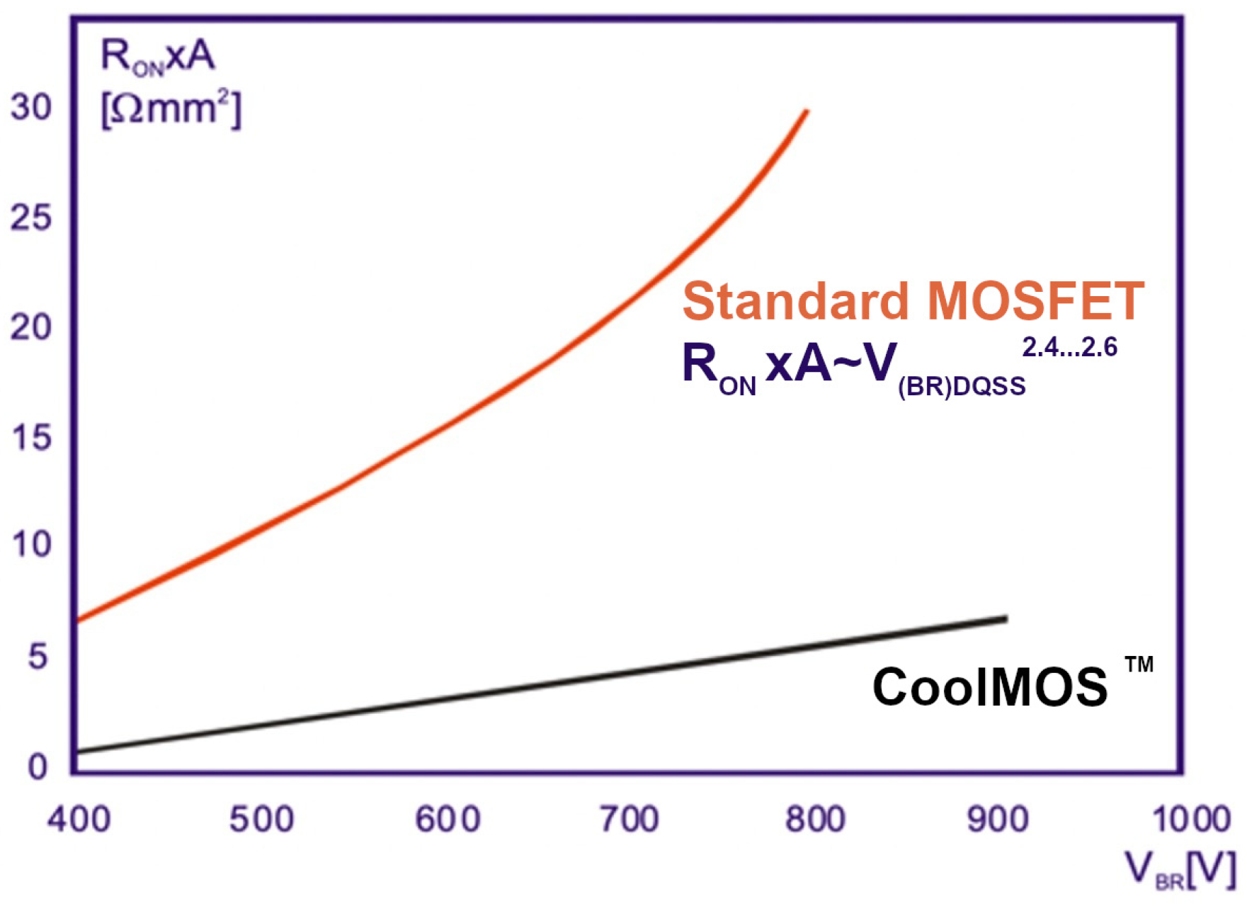
As a result, the direction of the electric field is also partially horizontal, the electric field can be spread evenly over both columns, and when the thickness of the columns is not too large, the superjunction effect occurs. It means that at the same blocking voltage, the doping of the n-layer, conducting current towards the drain, can be larger, which results in the lower transistor on-resistance. The prospective advantage of the CoolMOS™ construction over the VDMOS one is presented in many publications [3,4] in a highly convincing manner and is shown in Figure 2.
Though the CoolMOS™ idea was very promising, the rating parameters of the first devices introduced to the market in 1999 were not as attractive as one could expect. Since that time, their construction has been the subject of many investigations both theoretical, using simple analytical approaches [5,6,7,8,9,10,11] and equivalent circuit models [12,13], and numerical ones [14,15,16,17], dealing with particular aspects of superjunction application, as well as experimental works [18,19,20,21], resulting in new solutions, covering more intricate design, e.g., the one presented in overview paper [22]. However, until now, their maximum blocking voltage has not exceeded 800 V. One can suppose that it results from the fact that, although the CoolMOS™ basics are well known, the phenomena taking place inside manufactured devices limit their real possibilities. Unfortunately, this problem has so far only been addressed in the literature and has not been the subject of serious published investigations. This paper aims to better understand these phenomena, especially with respect to their run in the vicinity of any fabrication divergences in comparison to the CoolMOS™ concept. Part I is concentrated on the theoretical considerations aimed at identifying any physical constraints in the superjunction concept, whereas Part II of this paper gathers the results of a numerical investigation that takes advantage of Sentaurus TCAD (Synopsys Inc. Mountain View, CA, USA) [23], dealing with the influence of the divergences between the concept of ideal superjunction and the technology limitations on the real device work.
The theory of p-n superjunction has been outlined in [1,2], where some theoretical formulas were presented, but they were not extended to the phenomena in an ideal p-i-n diode, being the origin of its concept. This was conducted in Section II, dealing with the superjunction origin and resulting constraints. The solution was the subject of several numerical investigations [6,24], and it was applied in many manufactured device structures with the CoolMOS™ as the well-known commercial representative. However, nowhere have the constraints and consequences of the superjunction design been clearly taken out of the considered formulas and explicitly presented. Such knowledge is necessary when the limitations of the superjunction application are to be considered. It is presented below with respect to the specificity of CoolMOS™ design.

2. Materials

2.1. Superjunction Origin

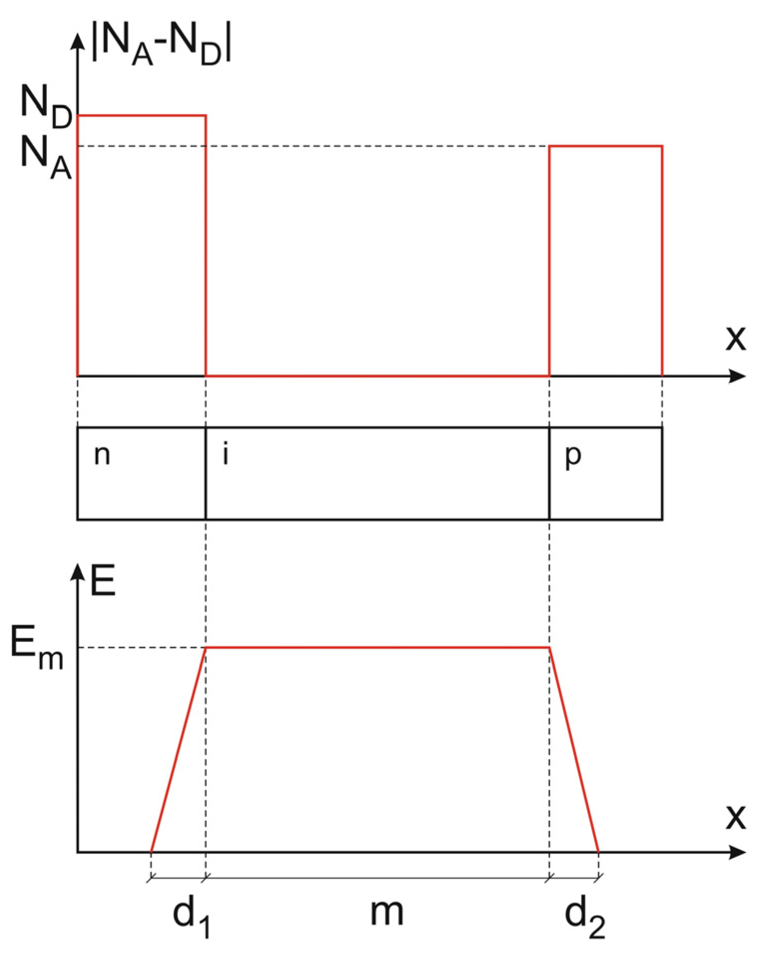
As the origin of the superjunction concept, one can consider the ideal p-i-n diode structure depicted in Figure 3. Its middle layer has no dominant dopants, so a no-space charge region can build up in it, which results in the constant electric field strength, Em, in the layer at the reverse bias condition. The changes in the electric field take place in the border n- and p-layers only, and the voltage drop VD over the whole reverse-biased diode is described by (1), where q is the electron charge, and ϵ is the material permittivity.
V D = V d 1 + V m + V d 2 = ϵ E m 2 2 q N D + m E m + ϵ E m 2 2 q N A = m + ϵ 2 1 N D + 1 N A E m E m
According to (1), the breakdown voltage of such an ideal p-i-n diode has no limits, since by keeping the magnitude Em below the electric field strength Ecrit, initiating the avalanche breakdown, one can achieve a safe blocking voltage just by increasing the width m of the middle layer that acts as the “no-charge flat field domain” (nc-FFD). Although the concept of the p-i-n diode with unlimited breakdown voltage is very exciting, unfortunately, it also has two significant weaknesses that definitely eliminate its application. Firstly, obtaining an ideal intrinsic semiconductor layer is very difficult; secondly, such a layer will have very large resistivity, leading to an unaccepted large diode on-resistance. Nevertheless, it shows that it is possible to design high voltage devices with the blocking voltage far beyond the limits determined by the critical electric field Ecrit [14,25]. It demands only to design the device in such a way that under the reverse bias conditions, an FFD layer with a flat electric field distribution along the voltage drop occurs.
In the case of an ideal p-i-n diode, the above condition is fulfilled by the i-layer that is completely free from any uncompensated built-in charge, particularly, from any dopants. Generally, it is impossible in doped materials, in which the presence of uncompensated charge (ions) results in a variation in the electric field. However, there are some exceptions to the above rule, when in some direction, no variation in electric field strength in the area with uncompensated charge can occur. One can distinguish between the two such situations presented below.

2.1.1. Built-In Charge Flat Field Domain (bcFFD)

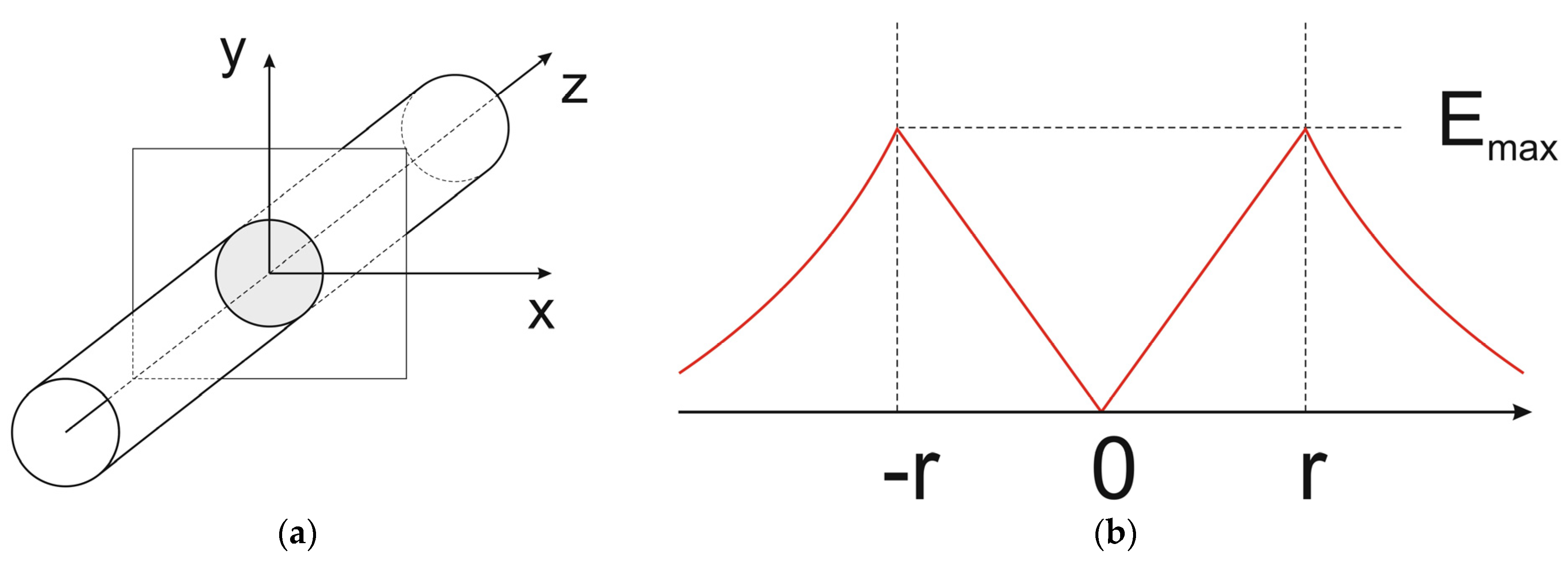
The situation takes place, e.g., in the infinite cylinder shown in Figure 4a with a homogeneous charge distribution. In any cross-section of the cylinder perpendicular to the z-axis, the same radially symmetrical electric field distribution with its maximal magnitude Emax on the cylinder surface shown in Figure 4b occurs, whereas the electric field strength along the z-axis is constant and, in particular, equal to zero on the z-axis. If the cylinder is terminated, e.g., by two semi-spheres like in Figure 5, the electric field distribution inside the cylinder changes a little, but in the central part of the cylinder, the region with constant electric field along the z-axis remains unchanged.
It means that when the external voltage drop between the semi-spheres is applied, the central part of the cylinder behaves as an FFD layer like the i-layer in a p-i-n diode in Figure 3. The only difference consists of the fact that, in the p-i-n diode, the constant magnitude of the electric field Em is at any point of the i-layer, whereas in the cylinder, each line parallel to the z-axis has its own constant magnitude of electric field.

2.1.2. Doped Semiconductor Flat Field Domain (dsFFD)

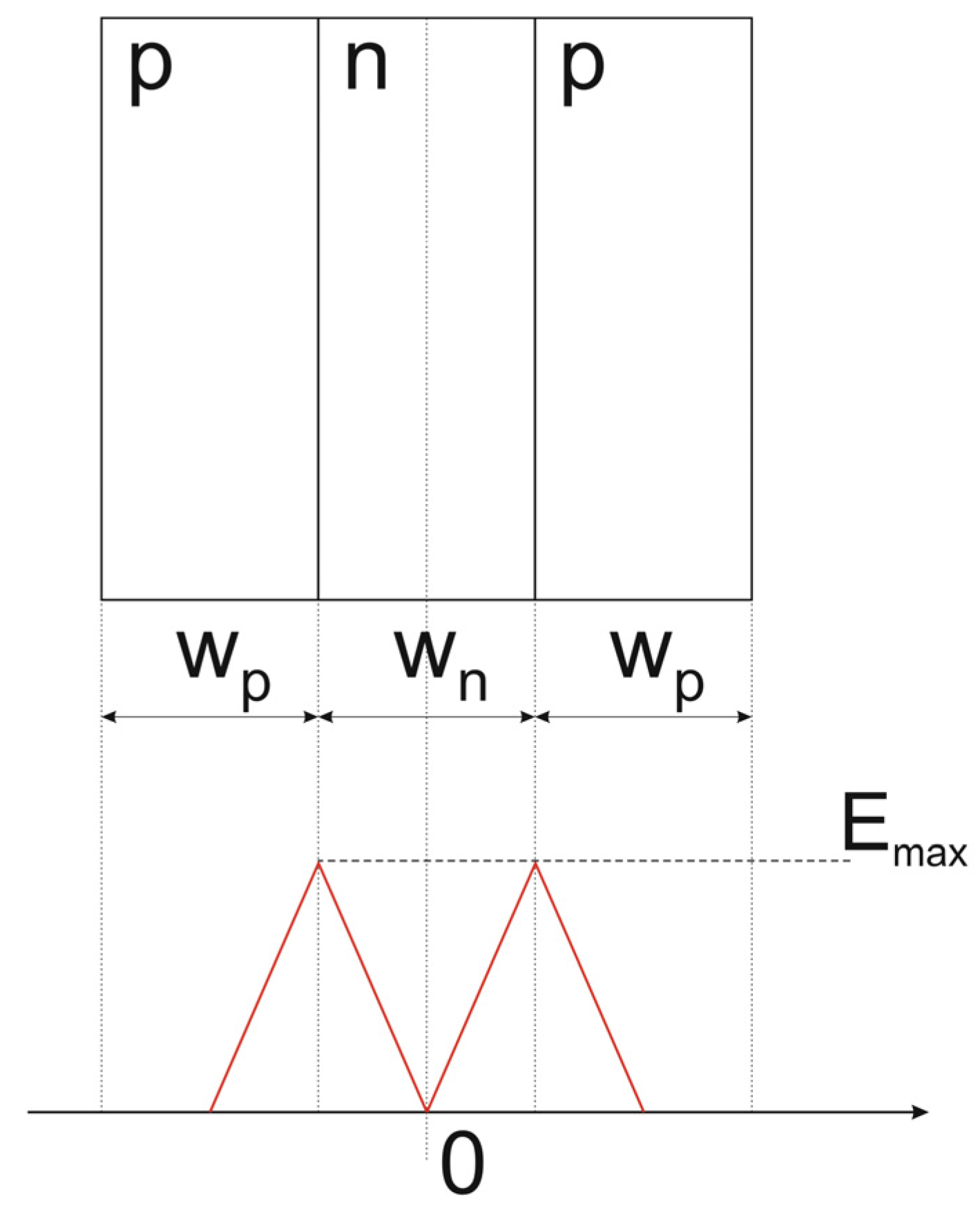
In doped semiconductors, the dsFFD, similar to the bcFFD shown in Figure 4, may be composed of two symmetric parallel p-n junctions having one common layer, e.g., an n-layer, as it is depicted in Figure 6. Its thickness wn is fixed to ensure that their SCRs (space charge regions) meet in the center, filling in the middle layer completely when the junctions are unbiased. As in the case of the cylinder in Figure 4, at the junction planes limiting the middle layer, the electrical field strength is maximal Emax, whereas inside the center (x = 0), its component along the junction planes is equal to zero. Depending on the type of middle layer, one can distinguish n- or p-type dsFFD. The dsFFD phenomenon can be employed to create a layer with a flat electric field distribution, necessary to obtain a high-voltage diode, and it is the basis for the superjunction concept. Note that the dsFDD phenomenon has a one-dimensional character and takes place only in a homogeneous doped domain limited by two parallel junctions. It allows to achievement of the flat component of the electrical field in the depletion area along lines parallel to the junction planes, when Emax is lower than the electric field strength Ecrit. In Figure 6, the depletion area covers the whole middle layer.

2.2. Superjunction Diode

The layers exhibiting the n- and p-type dsFFD ability are the bricks for a superjunction that is formed as a set of parallel pillars of the same length, n- and p-type by turns, terminated by n- and p-contact layers. It leads to the characteristic meander-like p-n junction shown in Figure 7a. The width of the pillars need not be the same but should be equal to or larger than the width of the middle layer in Figure 6, in which the dsFFD is built-in. In this case, the FFD appears just after the application of reverse bias. In the superjunction, each pillar acts as a separate p-i-n diode, from Figure 3, and can be analyzed separately.

2.2.1. Reverse Bias Ability

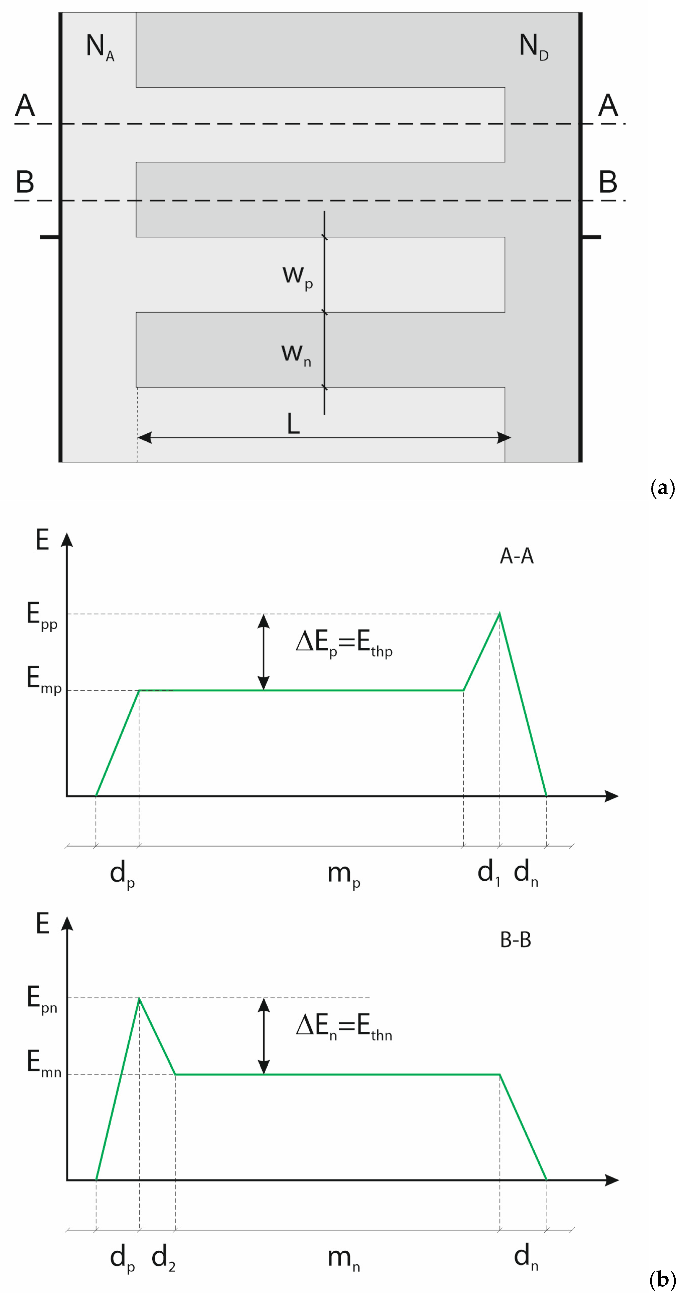
Generally, one can distinguish two stages in superjunction behavior under the reverse bias increase. The first represents the Normal Node (NM), when the electric field spreads over the pillars area, its strength is perpendicular to the junction plane, and no dsFFD area occurs. It finishes when the whole pillar areas are occupied by the electric field and the SCRs of opposite junctions meet in the pillar center, as in Figure 6. At this moment, the dsFFD area appears, the magnitude of the electric field strength at any point of the p-n junction plane is the same and defined as the threshold electric field Ethn in n-pillar or Ethp in p-pillar. Now, when the magnitudes of threshold electric fields are lower than the electric field strength corresponding to the avalanche breakdown Ecrit, the second stage, representing the SuperJunction Mode (SJM), starts to develop, like in the case of a p-i-n diode in Figure 3. In the SJM, due to the superjunction phenomenon, the electric field increases inside both pillars, keeping its flat distribution of magnitude Emn and Emp, respectively. It is shown in Figure 7b, presenting the electric field distribution at the SJM conditions in the planes A–A and B–B located in the middle of the p- and n-pillar, where d1 = 0.5wp and d2 = 0.5wn.
Taking into account the Poisson equation, one can evaluate the reverse voltage drop VSJp along the A–A axis:
V S J p = V d n + V d 1 + V m + V d p = E p p d n 2 + E p w p 4 + E m p w p 2 + E m p m p + E m p w p 2 = E p p d n 2 + E p w p 4 + E m p w p 2 + E p p E t h p m p + E m p w p 2
Taking advantage of the relations:
d n = ϵ E p p q N D
d p = ϵ E m p q N A
w p 2 = ϵ E p q N A
one can simply transform (2) into:
V S J p = ϵ E p p 2 2 q 1 N D + 1 N A + E p p E t h p m p
Similar considerations, performed for the n-pillar along the axis B–B in Figure 7, lead to a similar expression for the reverse voltage drop VSJn over the considered superjunction structure:
V S J n = ϵ E p n 2 2 q 1 N D + 1 N A + E n p E t h n m n
The derivation presented above of the Formulas (6) and (7) allows presenting very clearly the crux of the ideal superjunction concept in several items below:
  • Comparing (6), (7), and (1), one can notice that they are almost identical. They describe the same FFD phenomenon taking place in the diodes corresponding to p- and n-pillars of the superjunction diode in Figure 7 and the ideal p-i-n diode in Figure 3. Its presence leads to devices with generally unlimited blocking voltage. In the case of diodes corresponding to pillars in Figure 7, they can be formally considered as separate devices, although eventually they are aggregated into one device, which results in the identical length L and the identical maximal electrical field strength Epp = Epn. In the paper, the p-pillar diode is considered the main one, and next, the results are extended to the n-pillar diode.
  • According to (6) and (7), the reverse voltage drops, VSJp and VSJn, increase with the increase of mn and mp, whereas the maximum electric fields, Epp and Epn remain unchanged. For a symmetrical superjunction, in which NA = ND, one can simplify Equations (6) and (7), taking into account that d1 = d2, and mn = mp = m. Now they become identical: VSJp = VSJn = VSJ.
  • In the parallel pillar connection, the relation VSJn = VSJp must be kept at all times. Since the electric field strength on the junction plane is constant, the relation Epp = Epn is fulfilled. To obtain Ethn = Ethp = Eth, the construction of the diode must ensure that the dsFFD areas come out in both the pillars at the same bias.
  • In the pillars, the avalanche breakdown occurs when the maximum electric field, Epp or Epn, reaches the local critical magnitude Ecritp or Ecritn, which may locally differ, e.g., due to the changes in dopant concentration, as it is shown in Figure 8. So, the breakdown voltage for p- or n-pillar is:
V B p = ϵ E c r i t p 2 2 q 1 N D + 1 N A + E c r i t p E t h m p
V B n = ϵ E c r i t n 2 2 q 1 N D + 1 N A + E c r i t n E t h m n
  • The first element of Relations (8) and (9) corresponds to the breakdown voltage of a planar p-n junction, whereas the second one represents the complementary component introduced by the superjunction effect. It does not occur when Eth ≥ Ecrit, and the breakdown voltage is defined by the doping concentrations, NA and ND only. The superjunction component in (8) and (9) can be presented generally as:
    V B S J = E c r i t E t h m = E c r i t 1 E t h E c r i t m V B S J = E c r i t 1 γ m
    where γ = Eth/Ecrit ∈ <0;1>—the superjunction coefficient.
  • Introducing ∆Ep = Eth < Ecritp into (5), one can obtain the design condition ensuring the presence of the superjunction effect in the p-pillar:
N A w p < 2 ϵ E c r i t p q
  • Similar consideration performed for the n-pillar will result in a similar design condition, ensuring the presence of the superjunction effect in the n-pillar:
N D w n < 2 ϵ E c r i t n q
  • In Figure 7, the superjunction is formed as a parallel connection of several p- and n-pillars with their own breakdown voltages, VBp and VBn, respectively. Generally, they may be different when Ecritn ≠ Ecritp and the total superjunction breakdown voltage is equal to the lower pillar breakdown voltage VBp or VBn.
Introducing Ethp instead of ∆Ep into (5), one can obtain the relation between the threshold voltage Ethp and the p-pillar width wp and doping density NA. One can also obtain exactly the same relation for the n-pillar, which will cover the threshold voltage Ethn, the width wn, and the doping density ND. Since both relations are identical, one can consider them jointly using their general representation (13).
E t h = q N w 2 ϵ
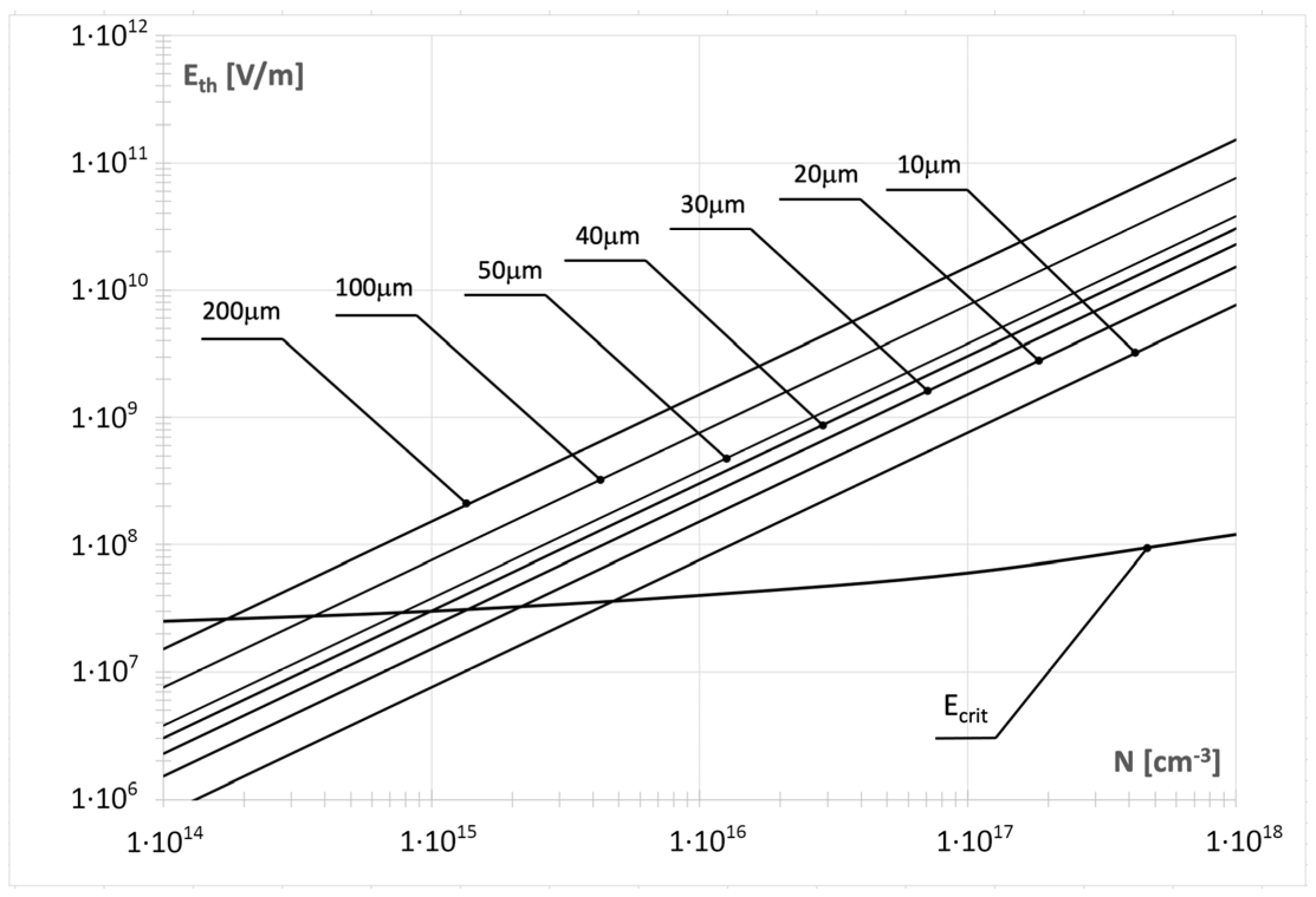
This analysis has been illustrated in Figure 8, where a set of linear characteristics Eth(N) for constant values of w was compared with the curve Ecrit(N), which represents the dependence of the critical electric field strength on the dopant concentration in silicon [13]. Each intersection point between the Ecrit(N) curve and the linear characteristics Eth(N) corresponding to a specific width w defines a condition in which the threshold electric field equals the critical electric field, Eth = Ecrit(N). At these points, the superjunction structure reaches its maximum efficiency, and the superjunction coefficient attains its highest value, γ = 1. In other words, these intersections mark the combinations of dopant concentration N and width w for which the superjunction effect fully contributes to the breakdown voltage, representing the ideal design condition for maximizing the performance of superjunction diodes.
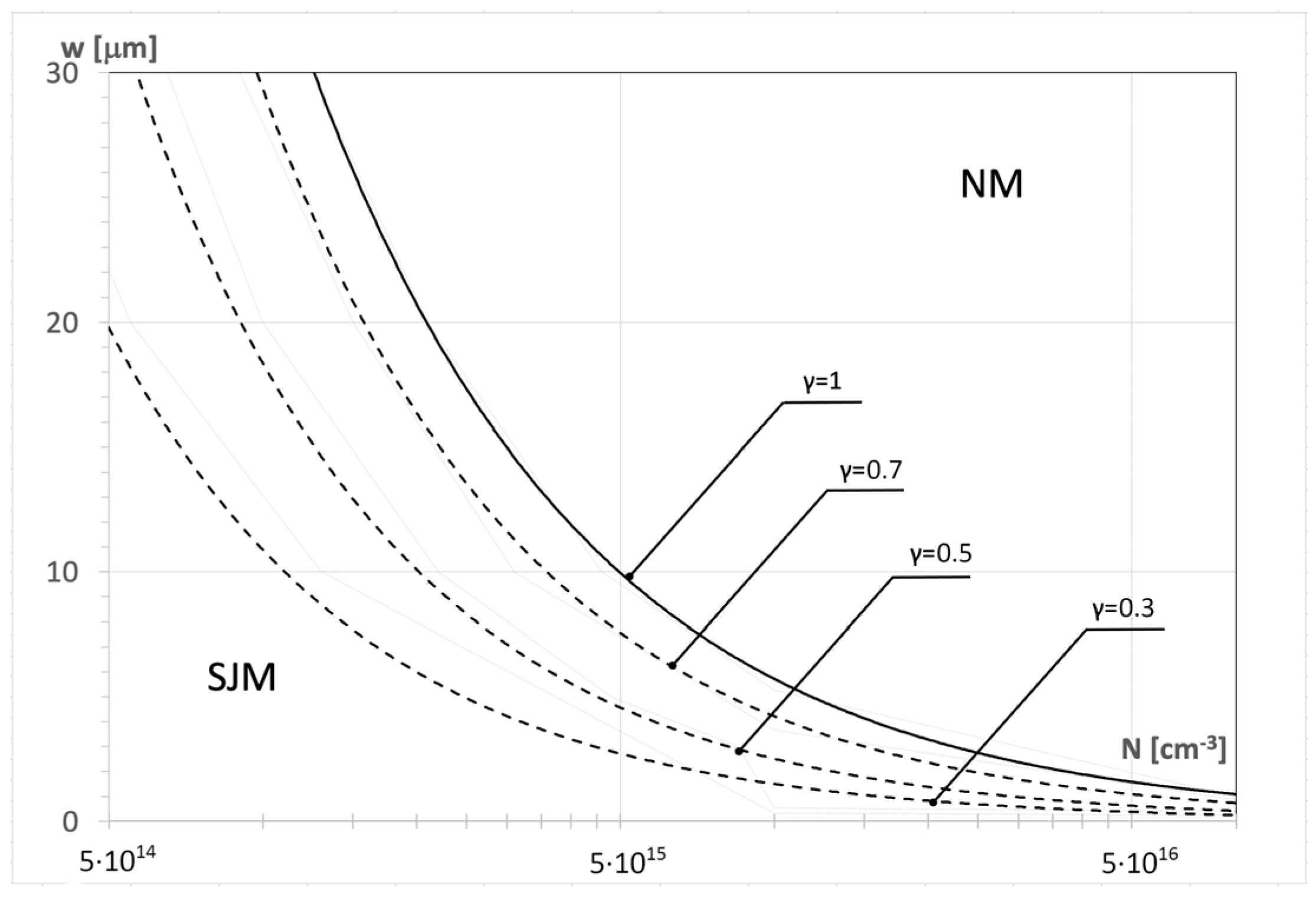
According to (10), it means that at the corresponding couples (N,w), the SJ electric field distribution already occurs, but corresponding to its superjunction compound VBSJ = 0. It is shown in a more useful way in Figure 9, which covers the curve presenting the relation between the dopant concentration N and the width w for γ = 1 (solid line). It divides the (N,w) domain into two parts. The bottom area, signed as SJM, gathers all the points (N,w) ensuring the design of diodes that can work in the superjunction mode with the superjunction component VBSJ > 0, whereas the upper area gathers the points corresponding to the diodes that, having the characteristic meander-like p-n junction shown in Figure 7a, can work in the normal mode only (NM).
Figure 9 can be an efficient tool supporting the SJ diode design when it is replenished by more curves drawn for a lower superjunction coefficient γ, as has been performed. Each curve in the figure corresponds to a different value of the coefficient γ, which determines the degree of superjunction contribution to the breakdown voltage. The curve for γ = 1 (solid line) defines the boundary for the maximum superjunction effect. The curves represent a set of points (N,w) ensuring the same Eth and the same blocking voltage VBSJ, depending on the assumed thickness m of the SJM area only.
The above consideration proves that, generally, there are no theoretical obstacles to obtaining the superjunction diode with an unlimited breakdown voltage defined by (8) and (9). Its design must, however, adhere to several restrictions that ensure the presence of FFD areas in the pillars and their proper development under reverse bias conditions:
  • In each pillar, the product N,w must correspond to a point inside the SJM region in Figure 9 to allow FFD areas to be built in.
  • The junction planes separating pillars must be parallel to ensure the flatness of the electric field inside the FFD areas.
  • To ensure the simultaneous development of the identical reverse voltage drop in the separated pillars, the magnitude of the electric field strength on the junction plane must be the same. It also concerns the threshold electric field Ethn, which, taking advantage of (13), leads to the restriction:
N D w n = N A w p
Let us notice that according to (8) and (9), the superjunction effect is more efficient when the threshold electric field Eth is small, which requires appropriately low-doped and narrow n- and p-pillars, to obtain the device length L and, following it, RON as small as possible.

2.2.2. Forward Bias Conditions

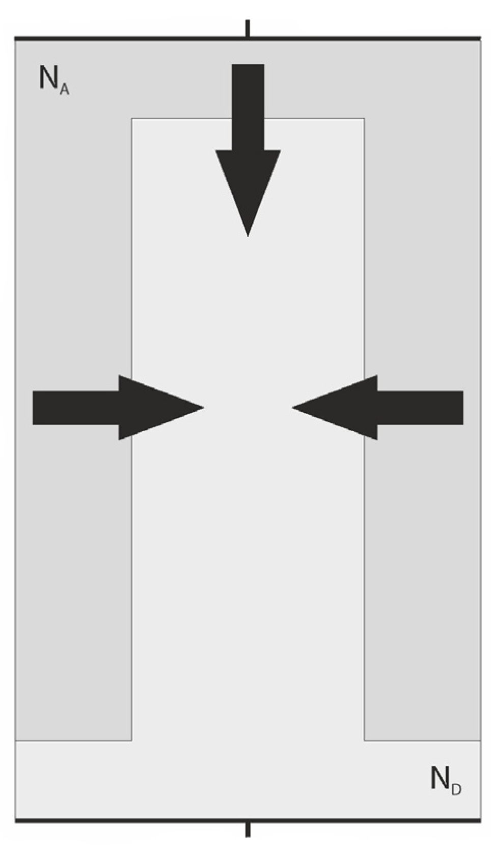
The forward-biased superjunction in Figure 7 can be considered as a parallel set of pillars with planar p-n junctions connected by vertical back p-n junctions limiting the pillars on both sides. It implicates the 2D character of current flow in the device since the vertical and lateral carrier injection occurs. Such a situation is shown in Figure 10 in the case of one n-pillar only, where the arrows indicate the hole injection. The holes injected by vertical junctions, as the excess minority ones, increase the total carrier concentration, causing the modulation of n-pillar conductance that noticeably increases when the concentration of injected holes is sufficiently large. It is accompanied by a decrease in voltage drop along the n-pillar.
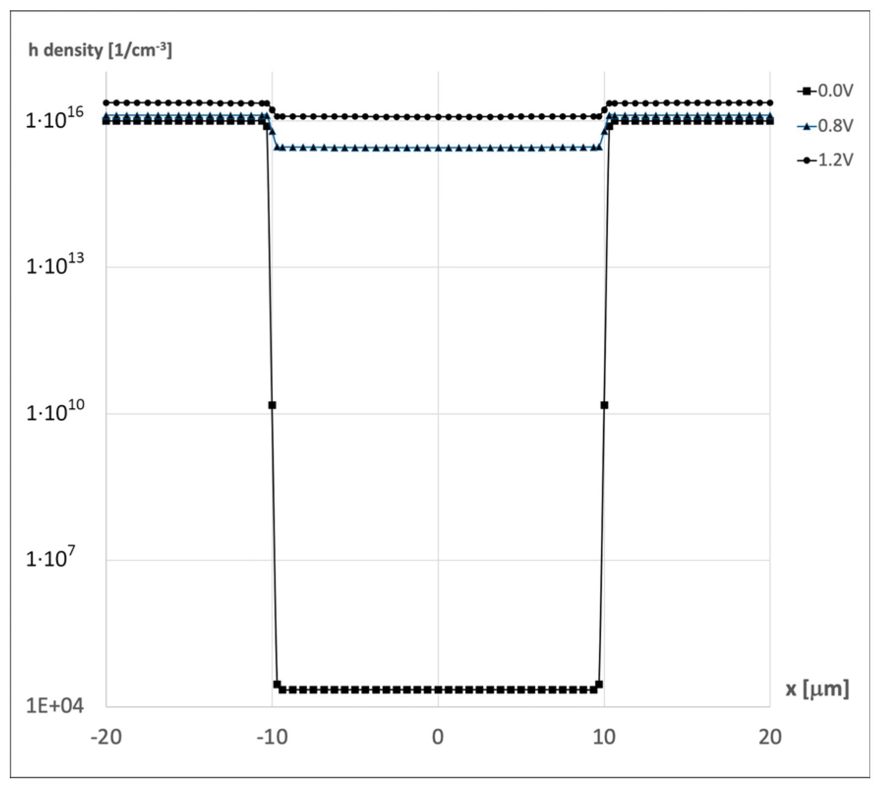
The above situation is illustrated by Figure 11. It presents the result of numerical simulation [26] showing the distribution of injected holes in the n-pillar when the n-pillar has the same doping as the p-pillar (NA = ND = 1·1016 cm−3).
It can therefore be stated that in superjunction devices, the modulation of the on-resistance RON occurs in the conducting state. Thanks to this modulation effect, the resistance decreases as the forward voltage increases.

2.3. Superjunction CoolMOS™ Transistor

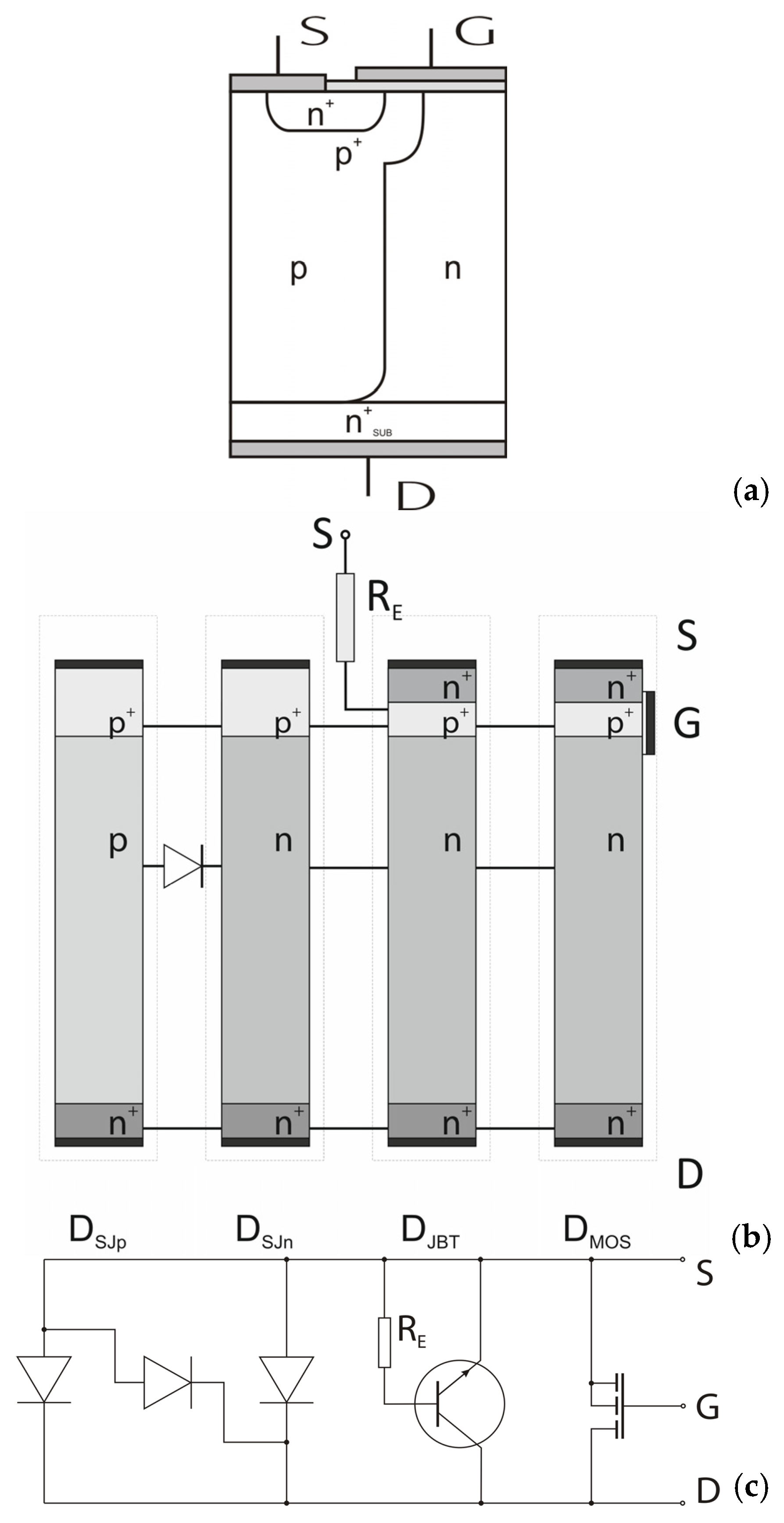
In the CoolMOS™ structure depicted in Figure 1, one can distinguish a bipolar high voltage rectifying superjunction diode and a unipolar lateral MOS transistor that is connected in series with the n-pillar of the diode, as it is shown in the equivalent circuit sketched in Figure 12. It covers four autonomous sections extracted from the p- and n-pillars, which are connected in parallel and represent different paths for the drain-source current flow.
The sections DSJn and DSJp represent these parts of p- and n-pillars that create the p-pillar and n-pillar diodes introduced directly between S and D contacts. They are permanently reverse-biased, and their breakdown voltage is determined by (8) and (9). The section DMOS covers the control MOS switch, allowing direct connection of the n+ source island and the n-pillar of the superjunction diode. When the switch is off, its breakdown voltage is determined by (9) if the channel length is sufficiently large. The Section DJBT covers the parasitic bipolar transistor whose collector layer n is also the n-pillar layer, whereas the base p+ is connected with the source contact, both through the emitter layer n+ and the resistor RE that reduces the effective emitter current. The reverse-biased collector junction keeps the section in a blocking state, but its reverse current is enlarged by the additional electron current injected from the n+ emitter. As a result, the density of electrons in the SCR layers of the collector junction essentially increases, and the avalanche breakdown develops at the lower electrical field strength EcritC = αEcrit, where α is in the range 0.5 ÷ 1 and depends on the details of the section DJBT design, i.e., the RE value. It leads to the lower breakdown voltage:
V B n C = ϵ E c r i t C 2 2 q 1 N D + 1 N A + E c r i t C E t h n m n
On the basis of the above considerations, one can theoretically evaluate the basic relation RONA versus VB for the CoolMOS™ design shown in Figure 2. For this goal, the following assumptions have been taken into account:
  • The CoolMOS™ forward current flows in the section DMOS only, which reduces the effective area of current flow to the n-pillar;
  • The CoolMOS™ breakdown voltage is limited to its lowest magnitude occurring in the section DJBT and is determined by Relation (15);
  • The first component of Relation (15) represents the breakdown of the planar p-n junction and is limited by the Ecrit, whereas the second one represents the superjunction effect and has no physical limits, and it is decisive mainly for the final breakdown voltage of CoolMOS™. Therefore, for simplicity, the Relation (15) can be reduced to the second component only:
V B = α E c r i t C E t h n m n
The effective CoolMOS™ on-resistance depends on the area of the n-pillar only and its magnitude, recalculated with respect to the device area A, is equal:
R O N A = m n q μ n N D w n + w p w n
and, taking into account the Relation (5) rearranged for n-pillar, it can be rewritten in the form:
R O N A = m n w n + w p 2 ϵ μ n E t h n
and considering (16), we can obtain the desired relation:
R O N A = V B w n + w p 2 ϵ μ n E t h n α E c r i t C E t h n
It is a linear dependence corresponding to the straight line in Figure 2, but it slightly differs from the relation presented in [2]. Its slope depends on the CoolMOS™ design parameters and can be both small or very large, which means that the relation between the lines for standard VDMOS and CoolMOS™ is not so unambiguous as it is shown in Figure 2. In some cases, the evaluated CoolMOS™ on-resistance may be even larger than the VDMOS one. To obtain low on-resistance, it is desired to keep a low magnitude of pillar widths and the threshold electric field strength Ethn, as well as a large coefficient α.

3. Discussion

CoolMOS™ has been considered a device to overcome the high-voltage limitations of unipolar power devices. Although theoretical considerations support this possibility, practical results have not confirmed it so far. This expectation appears to have been overly optimistic. The present analysis is devoted to identifying these limitations.
Until now, the run of physical phenomena inside superjunction structures has only been touched on in the literature. The theoretical considerations focus on achieving a deeper understanding of these phenomena and on identifying the physical limitations inherent in the superjunction concept. As a result, the first coherent presentation of the concept evolution, from its physical background to practical applications, has been created. Its idea arises from the conclusion that in the ideal p-i-n diode, its middle layer has no dominant dopants, and no space charge region can build up in it, which results in the constant value of the electric field strength Em in the layer. This way, the diode can block any voltage without the risk of avalanche breakdown when the middle intrinsic layer is sufficiently large. The only unacceptable disadvantage of such a high voltage diode is that its on-resistance is very large due to the lack of dopants in the middle layer.
This disadvantage can be eliminated by the introduction of dopants into the middle layer while keeping the flat electrical field distribution at the same time. It is possible to take advantage of the p-n superjunction concept, as it is shown in Figure 7. The superjunction diode is created as a set of parallel connected p-ν-n and p-π-n diodes, creating the characteristic meander-like p-n junction covering the set of n- and p-type pillars by turns. In such a design, the flatness of the electric field in the anode–cathode direction is ensured by side junctions between the pillars. Its theoretical analysis indicated that the superjunction effect is not an inherent feature of SJ diode design guaranteed by the meander-like p-n junction. According to (10), the superjunction component in the breakdown voltage VBSJ can only exist when the threshold electric field Eth defined by (13) is lower than the maximum electric field Ecrit corresponding to the avalanche breakdown in the considered semiconductor. Since Eth depends on the product (Nw), a supporting tool for designers in the form of a diagram in Figure 9 has been proposed. In the domain (N,w), two areas have been distinguished: SJM—gathers the points (N,w) ensuring the design of diodes with superjunction effect, and MN—gathers the points corresponding to diodes working in normal mode only.
The carried-out analytical consideration also follows the conclusions:
  • The superjunction diode constitutes a parallel connection of several p- and n-pillars with their own breakdown voltages.
  • The pillars’ junction planes need to be parallel to ensure the electric field remains uniform throughout the FFD regions.
  • The proper work of the SJ diode requires the symmetry in the pillars design that should fulfill Condition (14).
The CoolMOS™ takes advantage of the SJ idea and covers such a meander-like p-n junction that has been introduced to ensure high voltage capability, which means that any SJ limitations relate to it as well. The carried out theoretical investigations pointed out that, as it is shown in Figure 11, in the cell of CoolMOS™ structure, one can distinguish four elementary devices covering SJ elements, which are connected in parallel between S and D contacts. The section DMOS includes an n-pillar, and only it conducts the forward current. It means that at the symmetric design of SJ, the theoretical path of on-current flow is two times smaller than the area of the cell cross-section, which results in an increase in on-resistance. All the sections take part in the reverse voltage blocking, but the final breakdown voltage of their parallel connection is defined by the worst element. It is the section DBJT, including the bipolar transistor, whose breakdown voltage VBnC is limited by the resistor RE and equal to αVBn, where VBn—the breakdown voltage of n-column SJ and α is a bipolar transistor coefficient in the range 0.5 ÷ 1, depending on the details of section DJBT design. It means that the CoolMOS™ breakdown voltage can be twice as small as the breakdown voltage of the built-in SJ structure. It is also worth mentioning that according to (19), the relation RONA(VB) is linear as in Figure 2, but its slope depends on the CoolMOS™ design parameters. It can be both small or very large, which means that the relation between the lines for standard VDMOS and CoolMOS™ is not so unambiguous as it is shown in Figure 2.

4. Conclusions

Theoretical considerations indicate that, although CoolMOS™ is designed to alleviate high-voltage limitations in unipolar power devices, conceptual constraints prevent the realization of an ideal device without compromises. The introduction of superjunction elements increases breakdown voltage (VB) but also affects the on-state resistance (RON), mainly due to the reduced effective current path in the n-pillars and the presence of parasitic effects. Performance depends critically on the symmetry and proper design of pillar dimensions, as well as doping distribution and correct junction alignment. The breakdown voltage is limited by the weakest element in parallel-connected superjunction structures, including the bipolar transistor section. Achieving an optimal balance between low on-resistance and high breakdown voltage requires careful consideration of the theoretical limitations in both the superjunction and MOS control parts, emphasizing the need for thorough device design.

Author Contributions

Methodology, Z.L. and J.P.; software, J.P.; validation, Z.L. and J.P.; investigation, Z.L. and J.P.; resources, Z.L. and J.P.; writing—original draft preparation, Z.L.; visualization, J.P.; supervision, Z.L. All authors have read and agreed to the published version of the manuscript.

Funding

This research received no external funding.

Data Availability Statement

The original contributions presented in this study are included in the article. Further inquiries can be directed to the corresponding author.

Conflicts of Interest

The authors declare no conflicts of interest.

Abbreviations

The following abbreviations and symbols are used in this manuscript:
Abbreviations
SJSuperJunction
SJM SuperJunction Mode
NMNormal Mode
NA, NDdoping concentration in the p- and n-layer
E, Ecrit, Ethelectric field, critical electric field, threshold electric field
VSJreverse voltage drops in superjunction
VB, RONbreakdown voltage, on-resistance
wp, wna and n column width
Symbols
αbipolar transistor coefficient
γsuperjunction coefficient

References

  1. Fujihira, T. Theory of semiconductor superjunction devices. Jpn. J. Appl. Phys. 1997, 36, 6254–6262. [Google Scholar] [CrossRef]
  2. Chen, X.B.; Mawby, P.A.; Board, K.; Salama, C.A.T. Theory of novel voltage-sustaining layer for power devices. Microelectron. J. 1998, 29, 1005–1011. [Google Scholar] [CrossRef]
  3. Lorenz, L.; Maerz, M.; Deboy, G. CoolMOS—An important milestone towards a new power MOSFET generation. In Proceedings of the 38th International Power Conversion Conference PCIM’98, Nuremberg, Germany, 26–28 May 1998; pp. 151–160. [Google Scholar]
  4. Lorenz, L.; Deboy, G.; Knapp, A.; Marz, M. CoolMOS—A new milestone in high voltage power MOS. In Proceedings of the 11th International Symposium on Power Semiconductor Devices and ICs ISPSD’99, Toronto, ON, Canada, 26–28 May 1999; pp. 3–10. [Google Scholar] [CrossRef]
  5. Strollo, A.G.; Napoli, E. Power superjunction devices: An analytic model for breakdown voltage. Microelectron. J. 2001, 32, 491–496. [Google Scholar] [CrossRef]
  6. Strollo, A.G.; Napoli, E. Optimal on-resistance versus breakdown voltage tradeoff in superjunction power devices: A novel analytical model. IEEE Trans. Electron. Devices 2001, 48, 2161–2167. [Google Scholar] [CrossRef]
  7. Kondekar, P.; Patil, M.; Parikh, C. Analysis and design of super junction power MOSFET: CoolMOS for improved on resistance and breakdown voltage using theory of novel voltage sustaining layer. In Proceedings of the 23rd International Conference on Microelectronics, Nis, Serbia, 12–15 May 2002; pp. 209–212. [Google Scholar] [CrossRef]
  8. Podgórski, J. Analysis of New Structures of Unipolar Power Semiconductor Devices. Ph.D. Thesis, Lodz University of Technology, Lodz, Poland, 2003. [Google Scholar]
  9. Podgórski, J.; Lisik, Z. Numerical investigation of the CoolMOS features. In Proceedings of the 10th European Conference on Power Electronics and Applications EPE’2003, Toulouse, France, 2–4 August 2003. [Google Scholar]
  10. Saxena, T.; Khemka, V.; Qin, G.; Zitouni, M.; Gupta, R. Modeling and analysis of 3-D core-shell superjunction structures. IEEE Trans. Electron. Devices 2020, 68, 658–665. [Google Scholar] [CrossRef]
  11. Akshay, K.; Karmalkar, S. Optimum aspect ratio of superjunction pillars considering charge imbalance. IEEE Trans. Electron. Devices 2021, 68, 1798–1803. [Google Scholar] [CrossRef]
  12. Daniel, B.J.; Parikh, C.D.; Patil, M.B. Modeling of the CoolMOS transistor. II. DC model and parameter extraction. IEEE Trans. Electron. Devices 2002, 49, 923–929. [Google Scholar] [CrossRef]
  13. Kang, H.; Udrea, F. True material limit of power devices—Applied to 2D superjunction MOSFET. IEEE Trans. Electron. Devices 2018, 65, 1432–1439. [Google Scholar] [CrossRef]
  14. Langer, M.; Lisik, Z.; Podgórski, J. Numerical simulation of CoolMOS transistor, in Experience of Designing and Applications of CAD Systems in Microelectronics. In Proceedings of the 4th International Conference CADSM 2001, Lviv-Slavsko, Ukraine, 12–17 February 2001; pp. 303–304. [Google Scholar] [CrossRef]
  15. Lisik, Z.; Podgórski, J.; Raj, E. Numerical evaluation of the influence of technology incorrectness on CoolMOS features. In Proceedings of the International Conference Modern Problems of Radio Engineering, Telecommunications and Computer Science, Lviv-Slavsko, Ukraine, 24–28 February 2004; pp. 565–567. [Google Scholar]
  16. Fujihira, T.; Miyasaka, Y. Simulated superior performances of semiconductor superjunction devices. In Proceedings of the 10th International Symposium on Power Semiconductor Devices and ICs ISPSD’98, Kyoto, Japan, 3–6 June 1998; pp. 423–426. [Google Scholar] [CrossRef]
  17. Huang, H.; Hu, K.; Xu, W.; Xu, S.; Cui, W.; Zhang, W.; Ng, W.T. Numerical solutions for electric field lines and breakdown voltages in superjunction—Like power devices. IEEE Trans. Electron. Devices 2020, 67, 3898–3902. [Google Scholar] [CrossRef]
  18. Saito, W.; Omura, I.; Aida, S.; Koduki, S.; Izumisawa, M.; Yoshioka, H.; Okumura, H.; Yamaguchi, M.; Ogura, T. A 15.5 m Ω cm2-680V superjunction MOSFET reduced on-resistance by lateral pitch narrowing. In Proceedings of the 18th International Symposium on Power Semiconductor Devices and ICs ISPSD’06, Naples, Italy, 4–8 June 2006; pp. 293–296. [Google Scholar] [CrossRef]
  19. Sakakibara, J.; Noda, Y.; Shibata, T.; Nogami, S.; Yamaoka, T.; Yamaguchi, H. 600V-class super junction MOSFET with high aspect ratio P/N columns structure. In Proceedings of the 20th International Symposium on Power Semiconductor Devices and ICs ISPSD’08, Orlando, FL, USA, 18–22 May 2008; pp. 299–302. [Google Scholar] [CrossRef]
  20. Sugi, A.; Takei, M.; Takahashi, K.; Yajima, A.; Tomizawa, H.; Nakazawa, H. Super junction MOSFETs above 600V with parallel gate structure fabricated by deep trench etching and epitaxial growth. In Proceedings of the 20th International Symposium on Power Semiconductor Devices and ICs ISPSD’08, Orlando, FL, USA, 18–22 May 2008; pp. 165–168. [Google Scholar] [CrossRef]
  21. Vecino, E.; Stückler, F.; Pippan, M.; Hancock, J. First generation of 650V super junction devices with RDS(on)*A values below 1 Ω*mm2-best efficiency that keeps the ease-of-use and enables higher power ratings and frequencies. In Proceedings of the International Exhibition & Conference for Power Electronics. Intelligent Motion, Renewable Energy and Energy Management PCIM Europe’13, Nuremberg, Germany, 14–16 May 2013; pp. 621–628. [Google Scholar]
  22. Udrea, F.; Deboy, G.; Fujihira, T. Superjunction power devices, History, Development and Future Prospects. IEEE Trans. Electron. Devices 2017, 64, 713–727. [Google Scholar] [CrossRef]
  23. Synopsys. Sentaurus Manual; Synopsys, Inc.: Mountain View, CA, USA, 2022. [Google Scholar]
  24. Padmanabhan, K.; Guan, L.; Bobde, M.; Lui, S.; Bhalla, A.; Yilmaz, H.; Zhang, L. Self terminating lateral-vertical hybrid super-junction FET that breaks RDS·A—Charge balance trade-off window. In Proceedings of the IEEE 30th International Symposium on Power Semiconductor Devices and ICs ISPSD’18, Chicago, IL, USA, 13–17 May 2018; pp. 152–155. [Google Scholar] [CrossRef]
  25. Sze, S.M.; Li, Y.; Ng, K.K. Physics of Semiconductor Devices, 3rd ed.; John Wiley & Sons Inc.: Hoboken, NJ, USA, 2021. [Google Scholar]
  26. Lisik, Z.; Podgórski, J. On-resistance modulation in Super Junction Diode. In Proceedings of the 14th Conference on Electron Technology—ELTE 2023, Ryn, Poland, 18–21 April 2023. [Google Scholar]
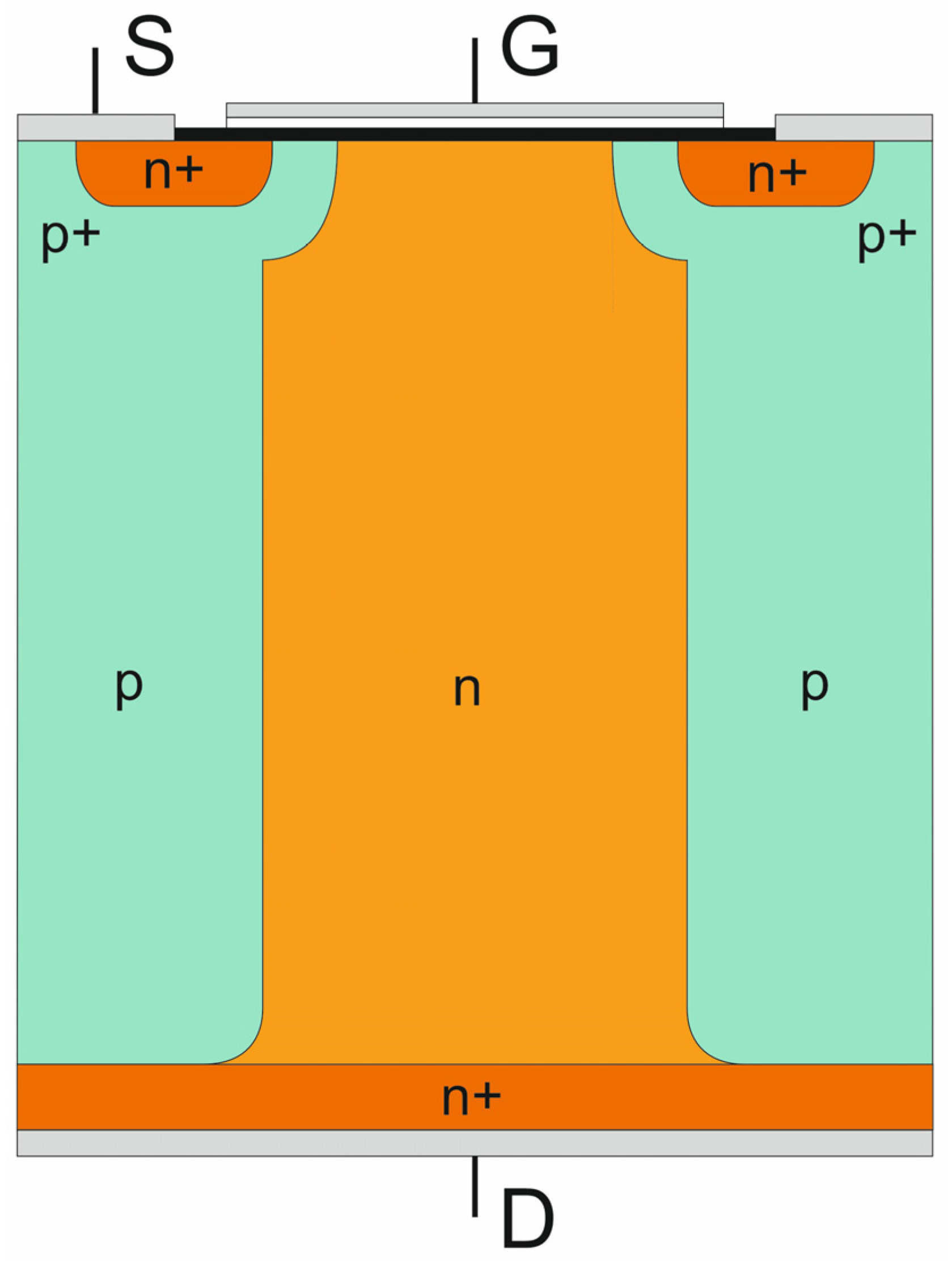
Figure 1. Basic cell of CoolMOS™ transistor.
Materials 18 05451 g001
Figure 2. Comparison of theoretical relations between on-resistance RonxA and blocking voltage VBR presented in [2] for standard MOSFET and CoolMOS™, respectively.
Materials 18 05451 g002
Figure 3. Ideal p-i-n diode: dopant concentration (upper) and electric field distribution (down).
Materials 18 05451 g003
Figure 4. Infinite cylinder covering homogeneous charge distribution (a) and corresponding electric field distribution along the x-axis in the sketched cross-section perpendicular to the z-axis (b).
Materials 18 05451 g004
Figure 5. Terminated cylinder covering homogeneous charge distribution (a) and corresponding electric field distribution along z-axis (b).
Materials 18 05451 g005
Figure 6. N-type dsFFD layer formed by two parallel symmetric p-n junctions.
Materials 18 05451 g006
Figure 7. Sketch of superjunction structure (a) and the distribution of electric field along of axis A–A and B–B in reverse biased superjunction (b).
Materials 18 05451 g007
Figure 8. Influence of dopant concentration on the threshold electric field strength Eth for different magnitudes of the width w and on the critical electric field strength Ecrit(N).
Materials 18 05451 g008
Figure 9. Definition of the superjunction mode (SJM) area in the (N,w) domain. The area for particular γ is below the corresponding curve (dashed line).
Materials 18 05451 g009
Figure 10. A section of the superjunction, with arrows indicating the directions of minority currents injected into the n-pillar—hole current at forward bias conditions.
Materials 18 05451 g010
Figure 11. Concentration of excess carriers along the Y–Y axis in the n-type pillar—VAC = 0 V; 0.8 V; 1.2 V.
Materials 18 05451 g011
Figure 12. Elementary CoolMOS™ cell: sketch of elementary cell (a), autonomous section distinguished in the cell (b), and equivalent circuit of the cell (c).
Materials 18 05451 g012
Disclaimer/Publisher’s Note: The statements, opinions and data contained in all publications are solely those of the individual author(s) and contributor(s) and not of MDPI and/or the editor(s). MDPI and/or the editor(s) disclaim responsibility for any injury to people or property resulting from any ideas, methods, instructions or products referred to in the content.