Constitutive Model of Secondary Annealing Behavior of Cu-Cu Joints in Cu/SiO2 Hybrid Bonding
Abstract
1. Introduction
2. Experiments
2.1. The Preparation of Cu/SiO2 Hybrid Bonding Structures
2.2. Secondary Annealing
2.3. Mechanical Properties Testing
2.4. Microstructural Characterization
3. Inversion Algorithm and Constitutive Modeling
- Step 1:
- Step 2:
- A = 0.010100n2 + 0.0017639n − 0.0040837
- B = 0.14386n2 + 0.018153n − 0.088198
- C = 0.59505n2 + 0.034074n − 0.65417
- D = 0.58180n2 − 0.088460n − 0.67290
- Step 3:
- Step 4:
4. Results and Discussion
4.1. Constitutive Behavior of Cu-Cu Joints
4.2. Microstructural Evolution of Cu-Cu Joints
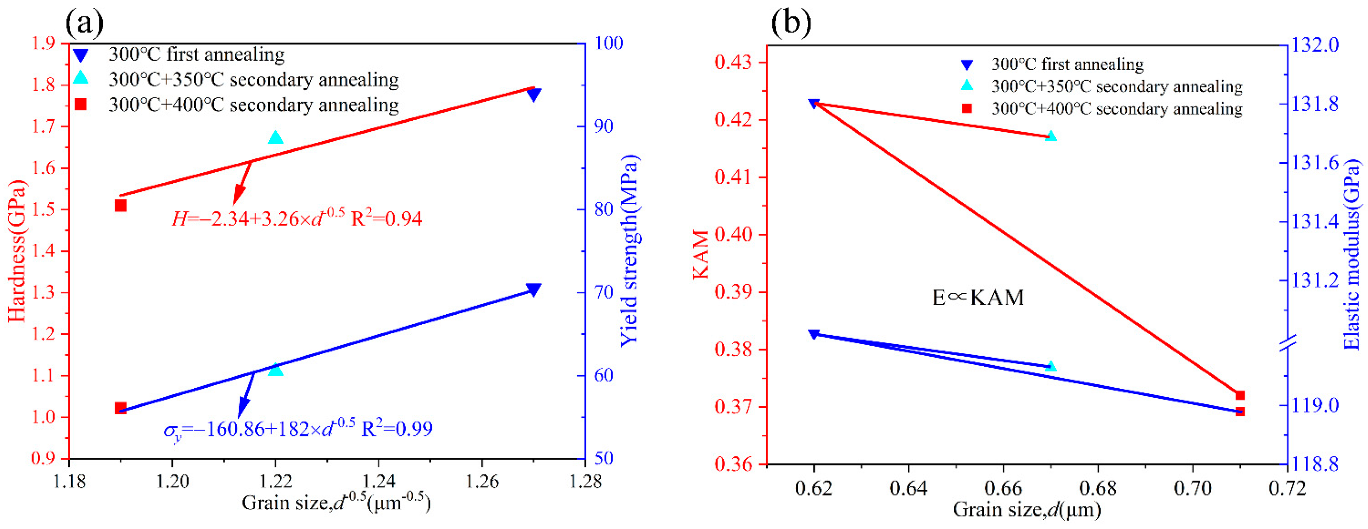
4.3. Micro–Macro Responses of Cu-Cu Joints
5. Conclusions
Author Contributions
Funding
Data Availability Statement
Conflicts of Interest
References
- Zhao, X.; Yuan, Y.; Wang, G.; Wang, C. Advances in Hybrid Bonding Technology for 3D Stacked Packages. Semicond. Technol. 2023, 48, 190–198. [Google Scholar]
- Liu, Y.; Zhang, H.; Dai, F. Advances in Cu/SiO2 wafer/level hybrid bonding technology for 3D integration applications. Microelectronics 2022, 52, 623–634. [Google Scholar]
- Jeon, C.; Kang, S.; Kim, M.E.; Park, J.; Kim, D.; Kim, S.; Kim, K.M. Ru passivation layer enables Cu–Cu direct bonding at low temperatures with oxidation inhibition. ACS Appl. Mater. Interfaces 2024, 16, 48481–48487. [Google Scholar] [CrossRef]
- Juang, J.-Y.; Lu, C.-L.; Li, Y.-J.; Tu, K.N.; Chen, C. Correlation between the microstructures of bonding interfaces and the shear strength of Cu-to-Cu joints using (111)-oriented and nanotwinned Cu. Materials 2018, 11, 2368. [Google Scholar] [CrossRef]
- Jang, E.J.; Kim, J.W.; Kim, B.; Matthias, T.; Park, Y.-B. Annealing temperature effect on the Cu-Cu bonding energy for 3D-IC integration. Met. Mater. Int. 2011, 17, 105–109. [Google Scholar]
- Chu, Y.C.; Chen, C. Anisotropic grain growth to eliminate bonding interfaces in direct copper-to-copper joints using <111>-oriented nanotwinned copper films. Thin Solid Film. 2018, 667, 55–58. [Google Scholar]
- Juang, J.Y.; Lu, C.L.; Chen, K.J.; Chen, C.-C.A.; Hsu, P.-N.; Chen, C.; Tu, K.N. Copper-to-copper direct bonding on highly (111)-oriented nanotwinned copper in no-vacuum ambient. Sci. Rep. 2018, 8, 13910. [Google Scholar] [CrossRef] [PubMed]
- Shie, K.-C.; Hsu, P.-N.; Li, Y.-J.; Tran, D.-P.; Chen, C. Failure Mechanisms of Cu–Cu bumps under thermal cycling. Materials 2021, 14, 5522. [Google Scholar] [CrossRef] [PubMed]
- Panchenko, I.; Wenzel, L.; Mueller, M.; Rudolph, C.; Hanisch, A.; Bartusseck, I.; Wolf, M.J. Microstructure development of Cu/SiO2 hybrid bond interconnects after reliability tests. IEEE Trans. Compon. Packag. Manuf. Technol. 2022, 12, 410–421. [Google Scholar]
- Panchenko, I.; Wambera, L.; Mueller, M.; Rudolph, C.; Hanisch, A.; Bartusseck, I.; Wolf, M.J. Grain structure analysis of Cu/SiO2 hybrid bond interconnects after reliability testing. In Proceedings of the 2020 IEEE 8th Electronics System-Integration Technology Conference (ESTC), Tonsberg, Norway, 15–18 September 2020; pp. 1–7. [Google Scholar]
- Lim, D.F.; Wei, J.; Leong, K.C.; Tan, C.S. Cu passivation for enhanced low temperature (≤300 °C) bonding in 3D integration. Microelectron. Eng. 2013, 106, 144–148. [Google Scholar] [CrossRef]
- Kang, Q.; Wang, C.; Zhou, S.; Li, G.; Lu, T.; Tian, Y.; He, P. Low-temperature Co-hydroxylated Cu/SiO2 hybrid bonding strategy for a memory-centric chip architecture. ACS Appl. Mater. Interfaces 2021, 13, 38866–38876. [Google Scholar] [CrossRef] [PubMed]
- Ni, Z.L.; Ma, J.S.; Liu, Y.; Li, B.H.; Wang, X.X.; Ye, F.X. Microstructure evolution and mechanical property strengthening mechanisms of Cu/Cu NPs/Cu joint fabricated by ultrasonic spot welding. Mater. Sci. Eng. A 2023, 866, 144656. [Google Scholar] [CrossRef]
- Sang, L.; Lu, J.; Wang, J.; Ullah, R.; Sun, X.; Zhang, Y.; Zhang, Z. In-situ SEM study of temperature-dependent tensile behavior of Inconel 718 superalloy. J. Mater. Sci. 2021, 56, 16097–16112. [Google Scholar]
- Raghavan, S.; Schmadlak, I.; Leal, G.; Sitaraman, S.K. Mixed-mode cohesive zone parameters for sub-micron scale stacked layers to predict microelectronic device reliability. Eng. Fract. Mech. 2016, 153, 259–277. [Google Scholar]
- Pshyk, O.; Nakonechna, O.; Coy, E. Current View of Nanoindentation: Recent Developments and Application in Material Characterization. ACS Appl. Mater. Interfaces 2025, 17, 36275–36300. [Google Scholar] [CrossRef]
- Chen, K.N.; Fan, A.; Reif, R. Microstructure examination of copper wafer bonding. J. Electron. Mater. 2001, 30, 331–335. [Google Scholar] [CrossRef]
- Chen, K.N.; Tan, C.S.; Fan, A.; Reif, R. Morphology and bond strength of copper wafer bonding. Electrochem. Solid/State Lett. 2003, 7, G14. [Google Scholar] [CrossRef]
- Chen, K.N.; Fan, A.; Tan, C.S.; Reif, R. Bonding parameters of blanket copper wafer bonding. J. Electron. Mater. 2006, 35, 230–234. [Google Scholar] [CrossRef]
- Oliver, W.C.; Pharr, G.M. An improved technique for determining hardness and elastic modulus using load and displacement sensing indentation experiments. J. Mater. Res. 1992, 7, 1564–1583. [Google Scholar] [CrossRef]
- Altmann, F.; Beyersdorfer, J.; Schischka, J.; Krause, M.; Franz, G.; Kwakman, L. Cross section analysis of Cu filled TSVs based on high throughput plasma/FIB milling. ASM Int. 2012, 39791, 39–43. [Google Scholar]
- Pelletier, H. Predictive model to estimate the stress–strain curves of bulk metals using nanoindentation. Tribol. Int. 2006, 39, 593–606. [Google Scholar] [CrossRef]
- Choi, Y.; Lee, H.; Kwon, D. Analysis of sharp/tip/indentation load/depth curve for contact area determination taking into account pile/up and sink/in effects. J. Mater. Res. 2004, 19, 3307–3315. [Google Scholar] [CrossRef]
- Wlanis, T.; Hammer, R.; Ecker, W.; Lhostis, S.L.; Sart, C.; Gallois-Garreignot, S.; Rebhan, B.; Maier, G.A. Cu/SiO2 hybrid bonding simulation including surface roughness and viscoplastic material modeling: A critical comparison of 2D and 3D modeling approach. Microelectron. Reliab. 2018, 86, 1–9. [Google Scholar] [CrossRef]
- Antunes, J.M.; Fernandes, J.V.; Menezes, L.F.; Chaparro, B.M. A new approach for reverse analyses in depth/sensing indentation using numerical simulation. Acta Mater. 2007, 55, 69–81. [Google Scholar] [CrossRef]
- Wu, W.; Qin, F.; An, T.; Chen, P. Experimental and numerical investigation of mechanical properties of electroplating copper filled in through silicon vias. IEEE Trans. Compon. Packag. Manuf. Technol. 2015, 6, 23–30. [Google Scholar] [CrossRef]
- Thakur, R.P.S.; Chhabra, N.; Ditali, A. Effects of wafer bow and warpage on the integrity of thin gate oxides. Appl. Phys. Lett. 1994, 64, 3428–3430. [Google Scholar] [CrossRef]
- Dao, M.; Chollacoop, N.; Van Vliet, K.J.; Süresh, S. Computational modeling of the forward and reverse problems in instrumented sharp indentation. Acta Mater. 2001, 49, 3899–3918. [Google Scholar] [CrossRef]
- Li, Y.; Chen, P.; Qin, F.; An, T.; Dai, Y.; Zhang, M.; Jin, Y. Constitutive modelling of annealing behavior in through silicon vias/copper. Mater. Charact. 2021, 179, 111359. [Google Scholar] [CrossRef]
- Lee, J.; Lee, C.; Kim, B. Reverse analysis of nanoindentation using different representative strains and residual indentation profiles. Mater. Des. 2009, 30, 3395–3404. [Google Scholar] [CrossRef]
- Petrov, I.; Barna, P.B.; Hultman, L.; Greene, J.E. Microstructural evolution during film growth. J. Vac. Sci. Technol. A Vac. Surf. Film. 2003, 21, S117–S128. [Google Scholar] [CrossRef]
- Zhang, W.; Li, S.Y.; Yang, Z.X.; Mao, Y.; Xu, S.Y. Microstructure evolution and mechanical properties of copper bonding wire during continuous annealing. Mater. Res. Innov. 2015, 19 (Suppl. S4), S225–S229. [Google Scholar] [CrossRef]
- Yu, L.L. Practical Handbook of Nonferrous Alloys; China Machiner Press: Beijing, China, 2002. [Google Scholar]
- Budiman, A.S.; Shin, H.A.S.; Kim, B.J.; Hwang, S.-H.; Son, H.-Y.; Suh, M.-S.; Chung, Q.-H.; Byun, K.-Y.; Tamura, N.; Kunz, M.; et al. Measurement of stresses in Cu and Si around through-silicon via by synchrotron X-ray microdiffraction for 3-dimensional integrated circuits. Microelectron. Reliab. 2012, 52, 530–533. [Google Scholar] [CrossRef]






| State | Elastic Modulus, E (GPa) | (MPa) | Hardening Exponent, n |
|---|---|---|---|
| 300 °C | 3.41 | 9.77 | 0.002 |
| 300 °C + 350 °C | 5.02 | 2.66 | 0.001 |
| 300 °C + 400 °C | 4.75 | 4.36 | 0.01 |
Disclaimer/Publisher’s Note: The statements, opinions and data contained in all publications are solely those of the individual author(s) and contributor(s) and not of MDPI and/or the editor(s). MDPI and/or the editor(s) disclaim responsibility for any injury to people or property resulting from any ideas, methods, instructions or products referred to in the content. |
© 2025 by the authors. Licensee MDPI, Basel, Switzerland. This article is an open access article distributed under the terms and conditions of the Creative Commons Attribution (CC BY) license (https://creativecommons.org/licenses/by/4.0/).
Share and Cite
Hao, Y.; Chen, S.; Li, C.; Chen, Z.; Qin, F.; Chen, P.; Tian, R.; Li, Z. Constitutive Model of Secondary Annealing Behavior of Cu-Cu Joints in Cu/SiO2 Hybrid Bonding. Materials 2025, 18, 5152. https://doi.org/10.3390/ma18225152
Hao Y, Chen S, Li C, Chen Z, Qin F, Chen P, Tian R, Li Z. Constitutive Model of Secondary Annealing Behavior of Cu-Cu Joints in Cu/SiO2 Hybrid Bonding. Materials. 2025; 18(22):5152. https://doi.org/10.3390/ma18225152
Chicago/Turabian StyleHao, Yiming, Si Chen, Chao Li, Zejian Chen, Fei Qin, Pei Chen, Renjie Tian, and Ziyang Li. 2025. "Constitutive Model of Secondary Annealing Behavior of Cu-Cu Joints in Cu/SiO2 Hybrid Bonding" Materials 18, no. 22: 5152. https://doi.org/10.3390/ma18225152
APA StyleHao, Y., Chen, S., Li, C., Chen, Z., Qin, F., Chen, P., Tian, R., & Li, Z. (2025). Constitutive Model of Secondary Annealing Behavior of Cu-Cu Joints in Cu/SiO2 Hybrid Bonding. Materials, 18(22), 5152. https://doi.org/10.3390/ma18225152


