
Optical and Photoconversion Properties of Ce3+-Doped (Ca,Y)3(Mg,Sc)2Si3O12 Films Grown via LPE Method onto YAG and YAG:Ce Substrates

 ,
, 
Abstract
1. Introduction
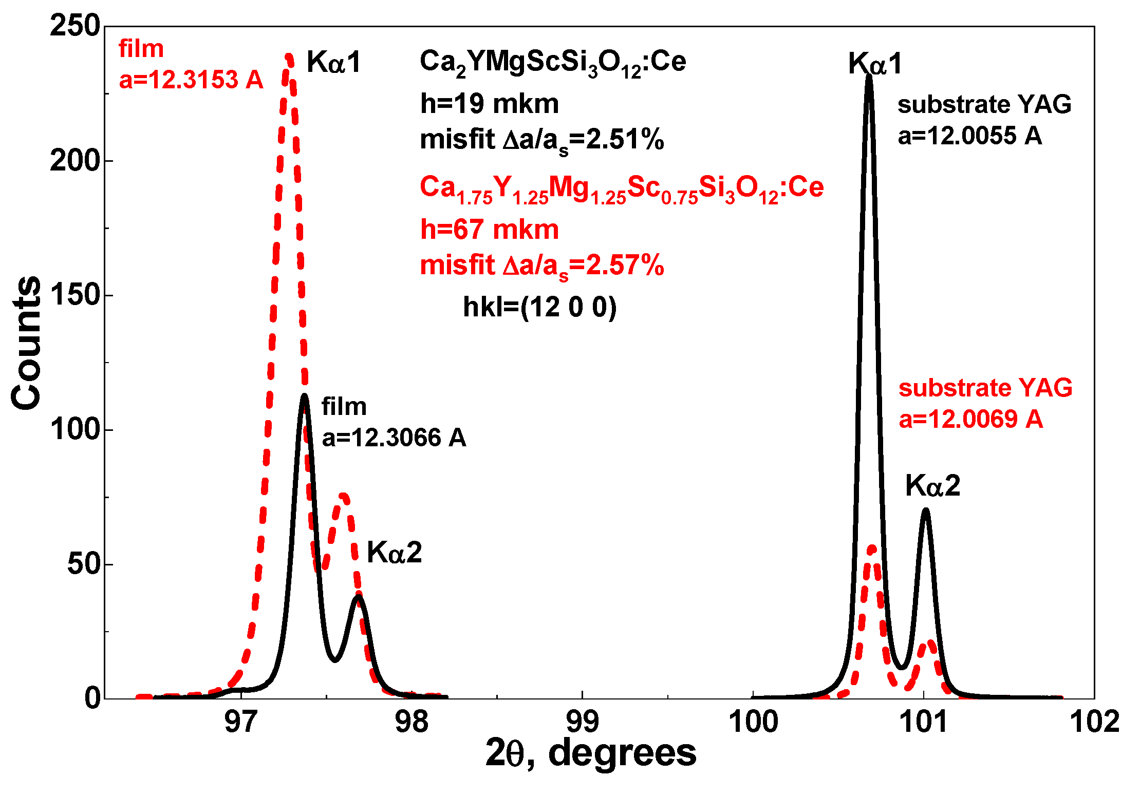
2. SCF Growth
3. Experimental Technique
4. Absorption and Luminescent Properties
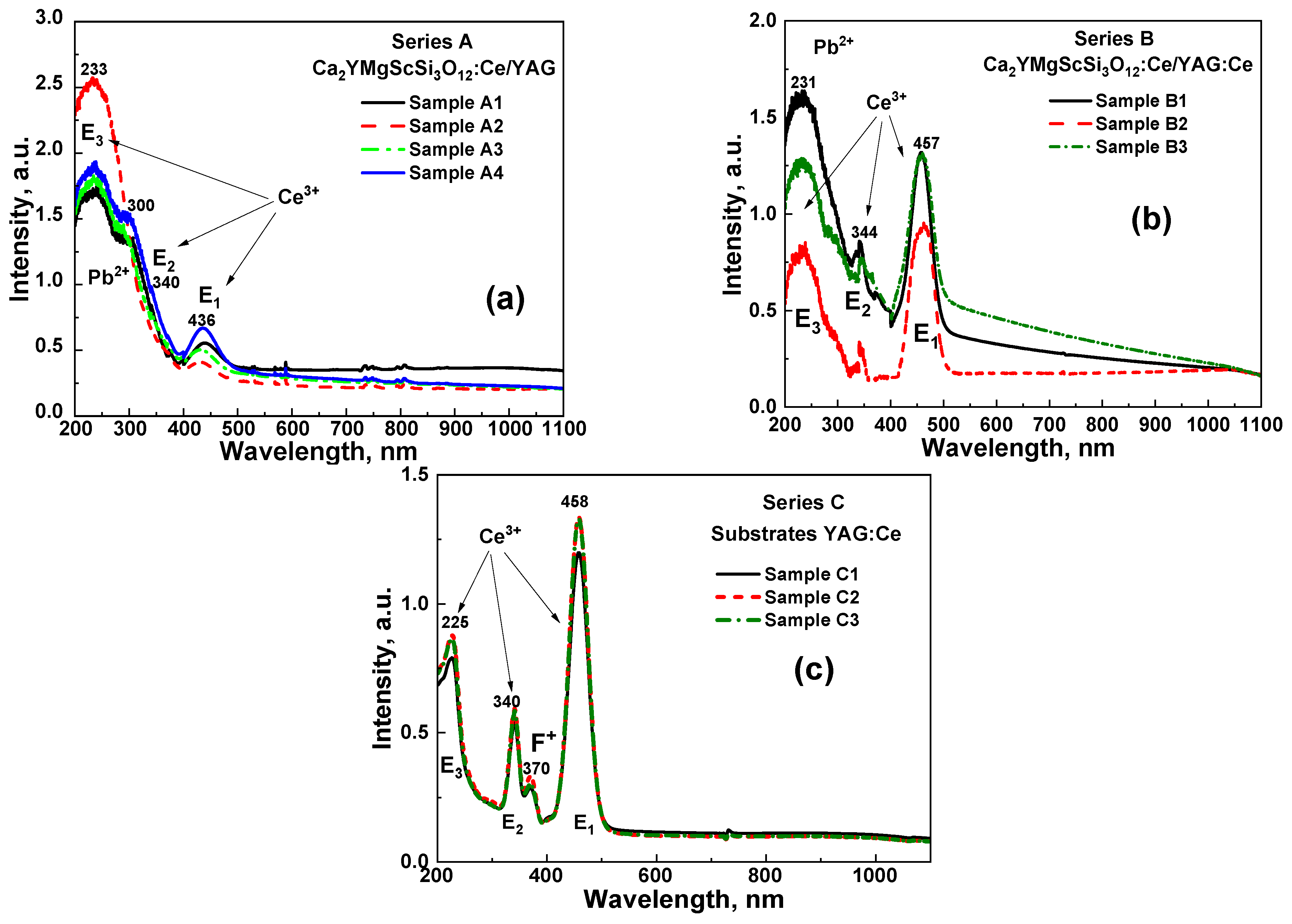
4.1. Absorption Spectra
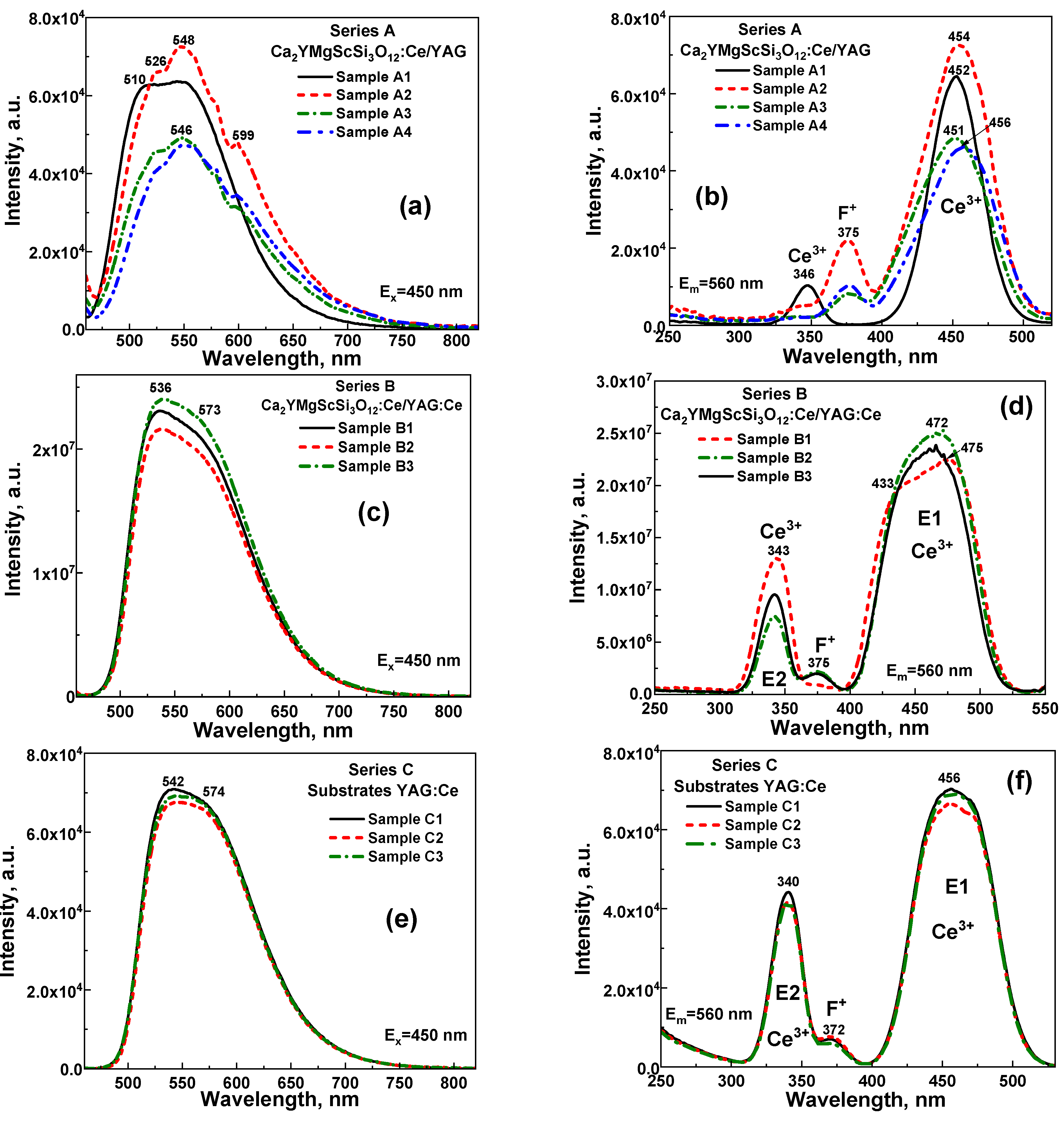
4.2. PL Spectra
4.3. PLE Spectra
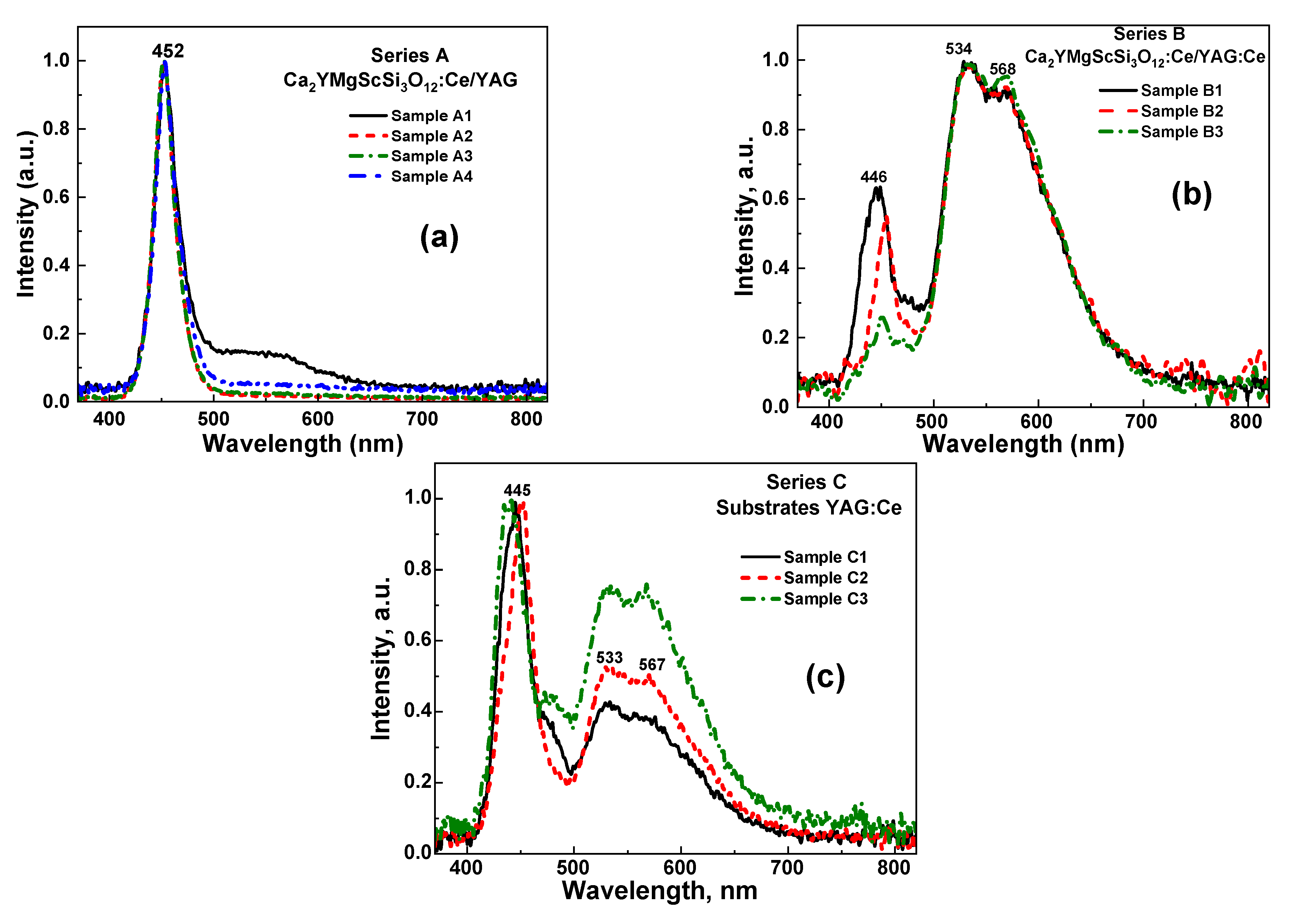
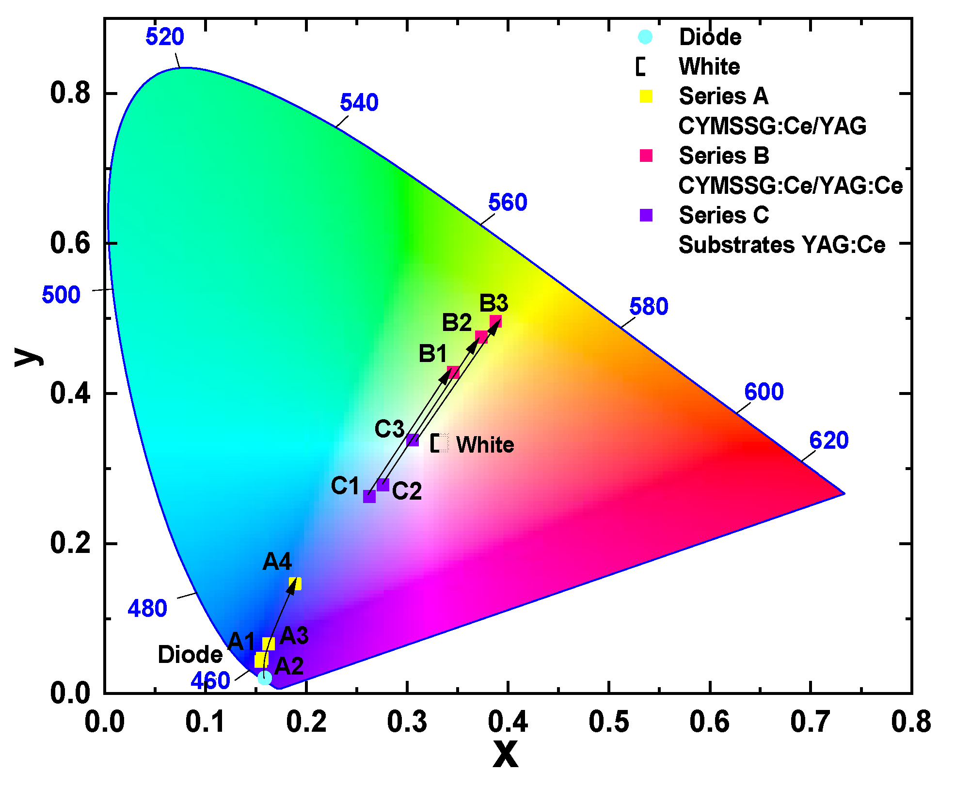
5. Photoconversion Properties
6. Conclusions
Author Contributions
Funding
Institutional Review Board Statement
Informed Consent Statement
Data Availability Statement
Conflicts of Interest
References
- Pimputkar, S.; Speck, J.S.; DenBaars, S.P.; Nakamura, S. Prospects for LED lighting. Nat. Photon. 2009, 3, 180–182. [Google Scholar] [CrossRef]
- Schubert, E.F.; Kim, J.K. Solid-State Light Sources Getting Smart. Science 2005, 308, 1274–1278. [Google Scholar] [CrossRef]
- Pust, P.; Schmidt, P.J.; Schnick, W. A revolution in lighting. Nat. Mater. 2015, 14, 454–458. [Google Scholar] [CrossRef]
- Sun, C.-C.; Chang, Y.-Y.; Yang, T.-H.; Chung, T.-Y.; Chen, C.-C.; Lee, T.-X.; Li, D.-R.; Lu, C.-Y.; Ting, Z.-Y.; Glorieux, B.; et al. Packaging efficiency in phosphor-converted white LEDs and its impact to the limit of luminous efficacy. J. Solid State Light. 2014, 1, 19. [Google Scholar] [CrossRef]
- Schlotter, P.; Schmidt, R.; Schneider, J. Luminescence conversion of blue light emitting diodes. Appl. Phys. A Mater. Sci. Amp. Process. 1997, 64, 417–418. [Google Scholar] [CrossRef]
- Nakamura, S.; Senoh, M.; Iwasa, N.; Nagahama, S.; Yamada, T.; Mukai, T. Superbright Green InGaN Single-Quantum-Well-Structure Light-Emitting Diodes. Jpn. J. Appl. Phys. 1995, 34, L1332. [Google Scholar] [CrossRef]
- Meng, Q.; Zhao, G.; Zhu, Q.; Li, X.; Sun, X.; Li, J.-G. Site-selective and cooperative doping of Gd3Al5O12:Ce garnets for structural stabilization and warm WLED lighting of low CCT and high CRI. Dalton Trans. 2022, 51, 645–654. [Google Scholar] [CrossRef]
- Lin, Y.-C.; Bettinelli, M.; Karlsson, M. Unraveling the Mechanisms of Thermal Quenching of Luminescence in Ce3+-Doped Garnet Phosphors. Chem. Mater. 2019, 31, 3851–3862. [Google Scholar] [CrossRef]
- Xia, Z.; Meijerink, A. Ce3+-Doped garnet phosphors: Composition modification, luminescence properties and applications. Chem. Soc. Rev. 2017, 46, 275–299. [Google Scholar] [CrossRef]
- Nishiura, S.; Tanabe, S.; Fujioka, K.; Fujimoto, Y. Properties of transparent Ce:YAG ceramic phosphors for white LED. Opt. Mater. 2011, 33, 688–691. [Google Scholar] [CrossRef]
- Bando, K.; Sakano, K.; Noguchi, Y.; Shimizu, Y. Development of high-bright and pure-white LED lamps. J. Light Vis. Environ. 1998, 22, 2–5. [Google Scholar] [CrossRef]
- Lee, H.-M.; Cheng, C.-C.; Huang, C.-Y. The synthesis and optical property of solid-state-prepared YAG:Ce phosphor by a spray-drying method. Mater. Res. Bull. 2009, 44, 1081–1085. [Google Scholar] [CrossRef]
- Huang, B.; Ma, Y.; Qian, S.; Zou, D.; Zheng, G.; Dai, Z. Luminescent properties of low-temperature-hydrothermally-synthesized and post-treated YAG:Ce (5%) phosphors. Opt. Mater. 2014, 36, 1561–1565. [Google Scholar] [CrossRef]
- Zhang, S.; Zhuang, W.; He, T.; Liu, Y.; Liu, R.; Gao, W.; Hu, Y.; Long, Z. Study on co-precipitation synthesized Y3Al5O12:Ce yellow phosphor for white LED. J. Rare Earths 2010, 28, 713–716. [Google Scholar] [CrossRef]
- Kang, Y.C.; Lenggoro, I.W.; Park, S.B.; Okuyama, K. YAG:Ce phosphor particles prepared by ultrasonic spray pyrolysis. Mater. Res. Bull. 2000, 35, 789–798. [Google Scholar] [CrossRef]
- Zhang, L.; Lu, Z.; Zhu, J.; Yang, H.; Han, P.; Chen, Y.; Zhang, Q. Citrate sol-gel combustion preparation and photoluminescence properties of YAG:Ce phosphors. J. Rare Earths 2012, 30, 289–296. [Google Scholar] [CrossRef]
- Gupta, K.V.K.; Muley, A.; Yadav, P.; Joshi, C.P.; Moharil, S.V. Combustion synthesis of YAG:Ce and related phosphors. Appl. Phys. B 2011, 105, 479–484. [Google Scholar] [CrossRef]
- Bierhuizen, S.; Krames, M.; Harbers, G.; Weijers, G. Performance and trends of high power light emitting diodes. In Proceedings of SPIE; Ferguson, I.T., Narendran, N., Taguchi, T., Ashdown, I.E., Eds. SPIE: Bellingham, WA, USA, 2007. [Google Scholar] [CrossRef]
- Allen, C.; Steckl, A.J. A nearly ideal phosphor-converted white light-emitting diode. Appl. Phys. Lett. 2008, 92, 143309. [Google Scholar] [CrossRef]
- Kim, Y.H.; Viswanath, N.S.M.; Unithrattil, S.; Kim, H.J.; Im, W.B. Review—Phosphor plates for high-power LED applications: Challenges and opportunities toward perfect lighting. ECS J. Solid State Sci. Technol. 2018, 7, R3134–R3147. [Google Scholar] [CrossRef]
- Fujita, S.; Sakamoto, A.; Tanabe, S. Luminescence characteristics of YAG glass—Ceramic phosphor for white LED. IEEE J. Sel. Top. Quantum Electron. 2008, 14, 1387–1391. [Google Scholar] [CrossRef]
- Víllora, E.G.; Arjoca, S.; Inomata, D.; Shimamura, K. Single-crystal phosphors for high-brightness white LEDs/LDs. In Proceedings of SPIE; Jeon, H., Tu, L.-W., Krames, M.R., Strassburg, M., Eds. SPIE: Bellingham, WA, USA, 2016. [Google Scholar] [CrossRef]
- Arjoca, S.; Víllora, E.G.; Inomata, D.; Aoki, K.; Sugahara, Y.; Shimamura, K. Temperature dependence of Ce:YAG single-crystal phosphors for high-brightness white LEDs/LDs. Mater. Res. Express 2015, 2, 055503. [Google Scholar] [CrossRef]
- Nizhankovskyi, S.V.; Tan’ko, A.V.; Savvin, Y.N.; Krivonogov, S.I.; Budnikov, A.T.; Voloshin, A.V. Single crystalline YAG:Ce phosphor for powerful solid-state sources of white light. The influence of production conditions on luminescence properties and lighting characteristics. Opt. Spectrosc. 2016, 120, 915–921. [Google Scholar] [CrossRef]
- Chao, W.-H.; Wu, R.-J.; Wu, T.-B. Structural and luminescent properties of YAG:Ce thin film phosphor. J. Alloys Compd. 2010, 506, 98–102. [Google Scholar] [CrossRef]
- Hsu, C.T.; Yen, S.K. Electrochemical synthesis of thin film YAG on inconel substrate. Electrochem. Solid State Lett. 2006, 9, D9. [Google Scholar] [CrossRef]
- Lee, Y.K.; Oh, J.R.; Do, Y.R. Enhanced extraction efficiency of Y2O3:Eu3+ thin-film phosphors coated with hexagonally close-packed polystyrene nanosphere monolayers. Appl. Phys. Lett. 2007, 91, 041907. [Google Scholar] [CrossRef]
- Bai, G.R.; Chang, H.L.M.; Foster, C.M. Erratum: “Preparation of single-crystal Y3Al5O12 thin film by metalorganic chemical vapor deposition”. Appl. Phys. Lett. 1994, 65, 790. [Google Scholar] [CrossRef]
- Díaz-Torres, L.A.; De la Rosa, E.; Salas, P.; Angeles-Chavez, C.; Arenas, L.B.; Nieto, J. Nanoparticle thin films of nanocrystalline YAG by pulsed laser deposition. Opt. Mater. 2005, 27, 1217–1220. [Google Scholar] [CrossRef]
- Mauk, M.G. Liquid-Phase Epitaxy. In Digital Encyclopedia of Applied Physics; Wiley: Hoboken, NJ, USA, 2023; pp. 1–31. [Google Scholar] [CrossRef]
- Capper, P.; Mauk, M. Liquid Phase Epitaxy of Electronic, Optical and Optoelectronic Materials; John Wiley & Sons: Hoboken, NJ, USA, 2007. [Google Scholar]
- Kundaliya, D.; Raukas, M.; Scotch, A.M.; Hamby, D.; Mishra, K.; Stough, M. Wavelength Converter for an LED and LED Containing. Same. Patent 8,937,332, 20 January 2015. [Google Scholar]
- Markovskyi, A.; Gorbenko, V.; Yokosawa, T.; Will, J.; Spiecker, E.; Batentschuk, M.; Elia, J.; Fedorov, A.; Pakuła, M.; Kaczmarek, M.; et al. Structural, luminescence and photoconversion properties of Lu3Al5O12:Ce single crystalline film phosphors for WLED application. J. Alloys Compd. 2022, 929, 167159. [Google Scholar] [CrossRef]
- Markovskyi, A.; Gorbenko, V.; Zorenko, T.; Yokosawa, T.; Will, J.; Spiecker, E.; Batentschuk, M.; Elia, J.; Fedorov, S.; Zorenko, Y. LPE growth of Tb3Al5O12:Ce single crystalline film converters for WLED application. CrystEngComm 2021, 23, 3212–3219. [Google Scholar] [CrossRef]
- VChani, I.; Yoshikawa, A.; Machida, H.; Fukuda, T. (Tb,Yb)3Al5O12 garnet: Crystal-chemistry and fiber growth by micro-pulling-down technique. Mater. Sci. Eng. B Solid State Mater. Adv. Technol. 2000, 75, 53–60. [Google Scholar] [CrossRef]
- Markovskyi, A.; Gorbenko, V.; Zorenko, T.; Witkiewicz-Lukaszek, S.; Sidletskiy, O.; Fedorov, A.; Zorenko, Y. Development of Three-Layered Composite Color Converters for White LEDs Based on the Epitaxial Structures of YAG:Ce, TbAG:Ce and LuAG:Ce Garnets. Materials 2023, 16, 1848. [Google Scholar] [CrossRef]
- Setlur, A.A.; Heward, W.J.; Gao, Y.; Srivastava, A.M.; Chandran, R.G.; Shankar, M.V. Crystal Chemistry and Luminescence of Ce3+-Doped Lu2CaMg2(Si,Ge)3O12 and Its Use in LED Based Lighting. Chem. Mater. 2006, 18, 3314. [Google Scholar] [CrossRef]
- Shimomura, Y.; Honma, T.; Shigeiwa, M.; Akai, T.; Okamoto, K.; Kijima, N. Photoluminescence and Crystal Structure of Green-Emitting Ca3Sc2Si3O12:Ce3+ Phosphor for White Light Emitting Diodes. J. Electrochem. Soc. 2007, 154, J35. [Google Scholar] [CrossRef]
- Katelnikovas, A.; Bettentrup, H.; Uhlich, D.; Sakirzanovas, S.; Jüstel, T.; Kareiva, A. Synthesis and optical properties of Ce3+-doped Y3Mg2AlSi2O12 phosphors. J. Lumin. 2009, 129, 1356. [Google Scholar] [CrossRef]
- Katelnikovas, A.; Bareika, T.; Vitta, P.; Jüstel, T.; Winkler, H.; Kareiva, A.; Žukauskas, A.; Tamulaitis, G. Y3−xMg2AlSi2O12: Cex3+ phosphors—Prospective for warm-white light emitting diodes. Opt. Mater. 2010, 32, 1261. [Google Scholar] [CrossRef]
- Katelnikovas, A.; Jurkevičius, J.; Kazlauskas, K.; Vitta, P.; Jüstel, T.; Kareiva, A.; Žukauskas, A.; Tamulaitis, G. Efficient cerium-based sol–gel derived phosphors in different garnet matrices for light-emitting diodes. J. Alloys Compd. 2011, 509, 6247. [Google Scholar] [CrossRef]
- Katelnikovas, A.; Ogiegło, J.M.; Winkler, H.; Kareiva, A.; Jüstel, T. Synthesis of Y3−xLuxAl3MgSiO12 garnet powders by sol–gel method. J. Sol-Gel Sci. Technol. 2011, 59, 311. [Google Scholar] [CrossRef]
- Katelnikovas, A.; Plewa, J.; Dutczak, D.; Möller, S.; Enseling, D.; Winkler, H.; Kareiva, A.; Jüstel, T. Synthesis and optical properties of green emitting garnet phosphors for phosphor-converted light emitting diodes. Opt. Mater. 2012, 34, 1195. [Google Scholar] [CrossRef]
- Katelnikovas, A.; Sakirzanovas, S.; Dutczak, D.; Plewa, J.; Enseling, D.; Winkler, H.; Kareiva, A.; Jüstel, T. Synthesis and optical properties of yellow emitting garnet phosphors for pcLEDs. J. Lumin. 2013, 136, 17. [Google Scholar] [CrossRef]
- Zhong, J.; Zhuang, W.; Xing, X.; Liu, R.; Li, Y.; Liu, Y.; Hu, Y. Synthesis, Crystal Structures, and Photoluminescence Properties of Ce3+-Doped Ca2LaZr2Ga3O12: New Garnet Green-Emitting Phosphors for White LEDs. J. Phys. Chem. C 2015, 119, 5562. [Google Scholar] [CrossRef]
- Pan, Z.; Xu, Y.; Hu, Q.; Li, W.; Zhou, H.; Zheng, Y. Combination cation substitution tuning of yellow-orange emitting phosphor Mg2Y2Al2Si2O12:Ce3+. RSC Adv. 2015, 5, 9489. [Google Scholar] [CrossRef]
- Cao, L.; Li, W.; Devakumar, B.; Ma, N.; Huang, X.; Lee, A.F. Full-Spectrum White Light-Emitting Diodes Enabled by an Efficient Broadband Green-Emitting CaY2ZrScAl3O12:Ce3+ Garnet Phosphor. ACS Appl. Mater. Interfaces 2022, 14, 5643–5652. [Google Scholar] [CrossRef] [PubMed]
- Huang, X.; Chan, J.; Chen, X. A well-performed green-emitting Lu1.5Ca1.5Al3.5Si1.5O12:Ce3+ garnet phosphor for high-quality pc-WLEDs. Ceram. Int. 2024, 50, 55979–55986. [Google Scholar] [CrossRef]
- Khaidukov, N.; Zorenko, T.; Iskaliyeva, A.; Paprocki, K.; Batentschuk, M.; Osvet, A.; Van Deun, R.; Zhydaczevskii, Y.; Suchocki, A.; Zorenko, Y. Synthesis and luminescent properties of prospective Ce3+ doped silicate garnet phosphors for white LED convertors. J. Lumin. 2017, 192, 328–336. [Google Scholar] [CrossRef]
- Levchuk, I.; Osvet, A.; Brabec, C.J.; Batentschuk, M.; Shakhno, A.; Zorenko, T.; Zorenko, Y. Micro-powder Ca3Sc2Si3O12:Ce silicate garnets as efficient light converters for WLEDs. Opt. Mater. 2020, 107, 109978. [Google Scholar] [CrossRef]
- Khaidukov, N.; Zorenko, Y.; Zorenko, T.; Iskaliyeva, A.; Paprocki, K.; Zhydachevskii, Y.; Suchocki, A.; Van Deun, R.; Batentschuk, M. New Ce3+ doped Ca2YMgScSi3O12 garnet ceramic phosphor for white LED converters. Phys. Rapid Res. Lett. 2017, 11, 1700016. [Google Scholar] [CrossRef]
- Xian, C.; Chen, X.; Huang, X. High-performance green-emitting Ca2YScAl2Si2O12:Ce3+ garnet phosphors and their applications in high-quality blue-chip-pumped white LEDs. J. Mater. Chem. C 2024, 12, 12378–12388. [Google Scholar] [CrossRef]
- Gorbenko, V.; Zorenko, T.; Paprocki, K.; Iskaliyeva, A.; Fedorov, A.; Schröppel, F.; Levchuk, I.; Osvet, A.; Batentschuk, M.; Zorenko, Y. Epitaxial growth of single crystalline film phosphors based on the Ce3+-doped Ca2YMgScSi3O12 garnet. CrystEngComm 2017, 19, 3689–3697. [Google Scholar] [CrossRef]
- Shakhno, A.; Gieszczyk, W.; Bilski, P.; Witkiewicz-Łukaszek, S.; Zorenko, T.; Cieszko, M.; Szczepański, Z.; Kotlov, A.; Zorenko, Y. Luminescence and photoconversion properties of Ce-doped Ca3Sc2Si3O12 crystal. J. Lumin. 2024, 266, 120311. [Google Scholar] [CrossRef]
- Zorenko, Y.; Batentschuk, M.; Brabec, C.; Osvet, A.; Gorbenko, V.; Levchuk, I.; Zorenko, T.; Chepyga, L.; Markovskiy, A.; Witkiewicz-Lukaszek, S. Patent Application EU EP 3831911A1 Composite Wavelength Converter. Application. EP19213887A, 5 December 2019. [Google Scholar]
- Shakhno, A.; Witkiewicz-Łukaszek, S.; Gorbenko, V.; Zorenko, T.; Zorenko, Y. Composite color converters based on the Ca3Sc2Si3O12:Ce single crystalline films. Opt. Mater. X 2024, 22, 100328. [Google Scholar] [CrossRef]
- Gorbenko, V.; Zorenko, T.; Witkiewicz-Łukaszek, S.; Shakhno, A.; Osvet, A.; Batentschuk, M.; Fedorov, A.; Zorenko, Y. Crystallization and Investigation of the Structural and Optical Properties of Ce3+-Doped Y3−xCaxAl5−ySiyO12 Single Crystalline Film Phosphors. Crystals 2021, 11, 788. [Google Scholar] [CrossRef]
- Zhu, J.; Sidletskiy, O.; Boyaryntseva, Y.; Grynyov, B. Structure and role of carbon-related defects in yttrium aluminum garnet. Opt. Mater. 2021, 11, 110561. [Google Scholar] [CrossRef]

| Sample | Nominal Content in the Melt | Measured SCF Composition | h, µm |
|---|---|---|---|
| A1 | Ca2YMgScSi3O12:Ce | Ca1.88Y1.09Ce0.01Mg0.9Sc1.42Si2.73O12 | 19 |
| A2 | Ca2YMgScSi3O12:Ce | Ca1.83Y1.08Ce0.03Mg0.9Sc1.51Si2.68O12 | 34 |
| A3 | Ca2YMgScSi3O12:Ce | Ca1.81Y1.12Ce0.03Mg0.93Sc1.48Si2.67O12 | 49 |
| A4 | Ca1.75Y1.25Mg1.25Sc0.75Si3O12:Ce | Ca1.63Y1.27Ce0.03Mg1.19Sc1.27Si2.72O12 | 67 |
| B1 | Ca2YMgScSi3O12:Ce | Ca1.92Y1.08Ce0.02Mg0.95Sc1.27Si2.78O12 | 10 |
| B2 | Ca1.75Y1.25Mg1.25Sc0.75Si3O12:Ce | Ca1.65Y1.35Ce0.03Mg1.18Sc0.61Si3.21O12 | 11 |
| B3 | Ca1.75Y1.25Mg1.25Sc0.75Si3O12:Ce | Ca1.68Y1.32Ce0.03Mg1.28Sc0.71Si3.01O12 | 22 |
| C1 | Y3Al5O12:Ce | Y2.99Ce0.01Al5O12 | 500 |
| C2 | Y3Al5O12:Ce | Y2.99Ce0.01Al5O12 | 500 |
| C3 | Y3Al5O12:Ce | Y2.988Ce0.012Al5O12 | 500 |
| Samples | SCF Thicknesses, µm | Type and Thicknesses of Substrate, mm | CIE Coordinates | CCT, K | CRI | LE,lm/W | |
|---|---|---|---|---|---|---|---|
| y | y | ||||||
| Series A | |||||||
| A1 | 19 | 0.5 | 0.162 | 0.066 | - | - | |
| A2 | 34 | 0.5 | 0.155 | 0.043 | - | - | |
| A3 | 49 | 0.5 | 0.156 | 0.047 | - | - | |
| A4 | 67 | 0.5 | 0.189 | 0.146 | - | - | |
| Series B | |||||||
| B1 | 10 | C1; 0.5 | 0.346 | 0.428 | 5150 | 62 | 102 |
| B2 | 11 | C2; 0.5 | 0.374 | 0.475 | 4612 | 59 | 112 |
| B3 | 22 | C3; 0.5 | 0.388 | 0.496 | 4406 | 59 | 115 |
| Series C | |||||||
| C1 | - | 0.5 | 0.263 | 0.263 | - | 78 | 71 |
| C2 | - | 0.5 | 0.276 | 0.278 | - | 75 | 72 |
| C3 | - | 0.5 | 0.305 | 0.338 | 6838 | 70 | 79 |
Disclaimer/Publisher’s Note: The statements, opinions and data contained in all publications are solely those of the individual author(s) and contributor(s) and not of MDPI and/or the editor(s). MDPI and/or the editor(s) disclaim responsibility for any injury to people or property resulting from any ideas, methods, instructions or products referred to in the content. |
© 2025 by the authors. Licensee MDPI, Basel, Switzerland. This article is an open access article distributed under the terms and conditions of the Creative Commons Attribution (CC BY) license (https://creativecommons.org/licenses/by/4.0/).
Share and Cite
Shakhno, A.; Gorbenko, V.; Zorenko, T.; Fedorov, A.; Zorenko, Y. Optical and Photoconversion Properties of Ce3+-Doped (Ca,Y)3(Mg,Sc)2Si3O12 Films Grown via LPE Method onto YAG and YAG:Ce Substrates. Materials 2025, 18, 3590. https://doi.org/10.3390/ma18153590
Shakhno A, Gorbenko V, Zorenko T, Fedorov A, Zorenko Y. Optical and Photoconversion Properties of Ce3+-Doped (Ca,Y)3(Mg,Sc)2Si3O12 Films Grown via LPE Method onto YAG and YAG:Ce Substrates. Materials. 2025; 18(15):3590. https://doi.org/10.3390/ma18153590
Chicago/Turabian StyleShakhno, Anna, Vitalii Gorbenko, Tetiana Zorenko, Aleksandr Fedorov, and Yuriy Zorenko. 2025. "Optical and Photoconversion Properties of Ce3+-Doped (Ca,Y)3(Mg,Sc)2Si3O12 Films Grown via LPE Method onto YAG and YAG:Ce Substrates" Materials 18, no. 15: 3590. https://doi.org/10.3390/ma18153590
APA StyleShakhno, A., Gorbenko, V., Zorenko, T., Fedorov, A., & Zorenko, Y. (2025). Optical and Photoconversion Properties of Ce3+-Doped (Ca,Y)3(Mg,Sc)2Si3O12 Films Grown via LPE Method onto YAG and YAG:Ce Substrates. Materials, 18(15), 3590. https://doi.org/10.3390/ma18153590