Abstract
In this study, Hf0.5Zr0.5O2 (HZO) thin-films were deposited using a Co-plasma atomic layer deposition (CPALD) process that combined both remote plasma and direct plasma, for the development of ferroelectric memory devices. Ferroelectric capacitors with a symmetric hybrid TiN/W/HZO/W/TiN electrode structure, incorporating W electrodes as insertion layers, were fabricated. Rapid thermal annealing (RTA) was subsequently employed to control the crystalline phase of the films. The electrical and structural properties of the capacitors were analyzed based on the RTA temperature, and the presence, thickness, and position of the W insertion electrode layer. Consequently, the capacitor with 5 nm-thick W electrode layers inserted on both the top and bottom sides and annealed at 700 °C exhibited the highest remnant polarization (2Pr = 61.0 μC/cm2). Moreover, the symmetric hybrid electrode capacitors annealed at 500–600 °C also exhibited high 2Pr values of approximately 50.4 μC/cm2, with a leakage current density of approximately 4 × 10⁻⁵ A/cm2 under an electric field of 2.5 MV/cm. The findings of this study are expected to contribute to the development of electrode structures for improved performance of HZO-based ferroelectric memory devices.
1. Introduction
Recently, the development of ferroelectric materials for applications in next-generation non-volatile memories and low-power transistors has gained considerable momentum. In particular, HfO2-based thin-films have attracted attention owing to their excellent compatibility with CMOS processes and their ability to exhibit ferroelectricity even at thicknesses of just a few nanometers [1,2,3,4]. Although the monoclinic (m-phase) structure—which is centrosymmetric and non-ferroelectric—is the thermodynamically stable phase of HfO2-based films at room temperature, phase transitions to the non-centrosymmetric orthorhombic (o-phase) with ferroelectric properties can occur in ultrathin films (~10 nm) owing to the relatively low kinetic barrier. Accordingly, extensive research has been conducted to promote o-phase formation through the optimization of the dopant type, annealing conditions, and electrode materials [5,6,7,8].
In a previous study, our research team deposited Hf0.5Zr0.5O2 (HZO) films using a Co-plasma atomic layer deposition (CPALD) process that simultaneously used both direct plasma (DP) and remote plasma (RP). We then analyzed the electrical properties of devices fabricated in a metal–ferroelectric–metal (MFM) structure based on these films [9]. The results showed that CPALD-deposited films exhibited a more efficient phase-transition to the ferroelectric o-phase during post-deposition annealing compared to films deposited via DPALD. Moreover, these films demonstrated higher remnant polarization and superior fatigue endurance characteristics. These improvements could be attributed to the high-energy radicals supplied during CPALD, which reduced the carbon residue while mitigating plasma-induced damage owing to the relatively mild plasma conditions.
One of the key factors in suppressing the m-phase and inducing a transition to the o-phase in HZO thin-films is the tensile stress and associated strain () imposed on the film by the mismatch in the thermal expansion coefficients (TECs) between the capping electrode material and the film during the cooling process after annealing. This relationship can be expressed as follows [10,11,12]:
where αfilm denotes the TEC of the film, αcap denotes the TEC of the electrode, and TA and RT denote the annealing temperature and room temperature, respectively.
To date, much research has focused on using single conductive nitride electrodes such as TiN—commonly used in semiconductor devices—to induce o-phase formation. However, TiN(α~9.4 × 10⁻⁶ K−1) has a relatively small TEC mismatch with HZO(α~10 × 10−6 K−1), limiting the stress-induced effect. Moreover, during annealing TiN can be prone to oxidation in the HZO deposition environment, leading to the formation of an interfacial TiOx layer which degrades the polarization stability and overall device performance [13,14,15,16,17].
Therefore, in this study the term hybrid electrode refers to a bilayer metal structure consisting of W and TiN, in which a low TEC W layer (α = 4.4 × 10⁻⁶ K−1) is inserted into the conventional MFM structure based on HZO films deposited by CPALD. A symmetric hybrid electrode configuration, TiN/W/HZO/W/TiN, was realized by applying the same W/TiN bilayer structure to both the top and bottom electrodes. This structural improvement aims to enhance electrical performance and facilitate future memory device applications. Initially, we analyzed the crystallographic phase and electrical properties of the films with respect to the annealing temperature in the presence of W insertion layers. Subsequently, we investigated how the thickness and arrangement of the W hybrid electrode influenced the structural and electrical characteristics of HZO-based ferroelectric capacitors.
2. Experimental Methods
To fabricate the MFM capacitor structure, a substrate consisting of a SiO2 (100 nm)/p-type Si wafer with a 50 nm-thick TiN bottom electrode was used. HZO thin-films were deposited on the substrate using a plasma-enhanced atomic layer deposition (PEALD, iOV-dx2, iSAC Research, Daejeon, Republic of Korea) system, applying the CPALD technique, which simultaneously used DP and RP discharges. For the deposition process, tetrakis(ethylmethylamino) hafnium (TEMAH, iChems, Hwaseong, Republic of Korea) and tetrakis(ethylmethylamino) zirconium (TEMAZ, iChems, Hwaseong, Republic of Korea) were used as the Hf and Zr precursors, respectively. Alternating ALD cycles of HfO2 and ZrO2 were applied to achieve a 1:1 ratio, forming a 10 nm-thick HZO thin-film. The deposition temperature was maintained at 240 °C, and O2 was used as the reactant gas. During the reactant gas injection process, the DP was activated by applying 100 W RF power for 2 s through a plasma generator inside the chamber, whereas the RP was simultaneously activated using an external remote plasma system (RPS, En2ra-RPS, EN2CORE Technology, Daejeon, Republic of Korea), applying 2.6 kW power for 12 s to generate a high-density plasma. The top electrode was fabricated via a lift-off process to form 200 μm-diameter, 50 nm-thick, dot-shaped TiN single electrodes or W/TiN hybrid electrodes, using RF magnetron sputtering. When introducing a W insertion layer above the HZO ferroelectric film, the W layer was deposited first, followed by in situ TiN deposition. By varying the W insertion layer thickness from 0 to 20 nm, a symmetric hybrid TiN/W/HZO/W/TiN ferroelectric capacitor structure was fabricated, as illustrated in Figure 1. Finally, rapid thermal annealing (RTA) was performed to crystallize the film using a nitrogen atmosphere at temperatures ranging from 500 to 700 °C for 30 s.
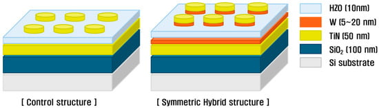
Figure 1.
Schematic of an MFM capacitor structure with a W insertion electrode layer.
The crystallinity of the HZO thin-films deposited by CPALD was analyzed using X-ray diffraction (XRD, SmartLab, Rigaku, Tokyo, Japan), and the chemical bonding states were examined by X-ray photoelectron spectroscopy (XPS, AXIS-NOVA, Manchester, UK). The cross-sectional morphology and crystallization of the films were observed using field emission transmission electron microscopy (FE-TEM, JEM-2100F, JEOL, Tokyo, Japan). For electrical characterization of the fabricated MFM devices, a semiconductor parameter analyzer (4200-SCS, Keithley, Cleveland, OH, USA) connected to a microprobe station (APX-6B, WIT Co., Suwon, Republic of Korea) was used to measure the P–E (polarization–electric field) hysteresis curves and I–V (current–voltage) curves. Measurements were conducted using a ±3 V triangular pulse at 1 kHz frequency, and measurements were taken before and after 104 cycles to account for the wake-up effect of the films [18,19].
3. Results and Discussion
Figure 2 presents the electrical characteristics of capacitors with a symmetric hybrid TiN/W/HZO/W/TiN electrode structure, where 10 nm-thick W insertion electrodes were incorporated at both the top and bottom interfaces of the HZO layer. The devices were subjected to post-deposition annealing at various temperatures. Figure 2a,b show the P–E hysteresis loops in the pristine state and after 104 wake-up cycles, respectively. Devices with the W insertion layers exhibited excellent ferroelectric behavior in the pristine state regardless of the annealing temperature, with 2Pr values ranging from 43 to 52 μC/cm2. Upon wake-up cycling, the remnant polarization and coercive field increased, producing ideal square-shaped hysteresis loops. Notably, the sample annealed at 700 °C exhibited the highest remnant polarization with a 2Pr of 60.5 μC/cm2.
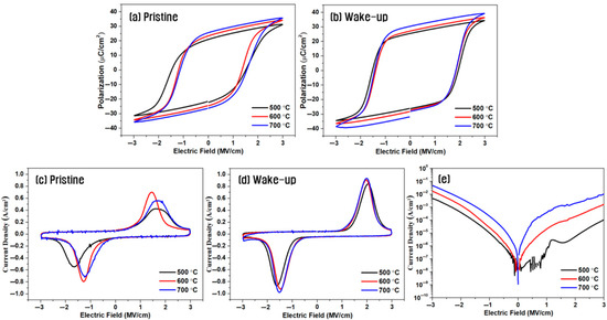
Figure 2.
P–E hysteresis loops (a,b), switching current (c,d), and leakage current (e) of capacitors with a symmetric hybrid TiN/W/HZO/W/TiN structure with a 10 nm-thick W insertion layer at various annealing temperatures; (a,c) in the pristine state and (b,d) in the wake-up state.
Figure 2c,d show the corresponding switching current density curves. Symmetrical double switching peaks were already evident before wake-up, and well-defined switching current peaks appeared near the coercive field (Ec) after wake-up cycling, indicating enhanced ferroelectric performance.
Figure 2e shows the leakage current characteristics of the same samples as a function of annealing temperature. The leakage current slightly increased with higher annealing temperatures, likely owing to the diffusion of W metal species and increased oxygen vacancy concentration, promoting charge transport along the grain boundaries [20,21].
Figure 3 shows the effect of varying the thickness of the W insertion layer on the electrical properties of capacitors with the symmetric electrode structure annealed at 700 °C. As shown in Figure 3a,b, the device without W insertion exhibited a 2Pr of 27.8 μC/cm2 in the pristine state, which increased to 36.7 μC/cm2 after 104 wake-up cycles. By contrast, the hybrid electrode device with a 5 nm-thick W layer exhibited a high 2Pr of 51.2 μC/cm2 even before wake-up, which further increased to 61.0 μC/cm2 after wake-up—the highest value observed in this study. With a 10 nm-thick W insertion layer the 2Pr remained high at 60.5 μC/cm2 after wake-up, whereas with a 20 nm-thick layer the value decreased slightly to 55.4 μC/cm2. This decline could be attributed to the emergence of bulk-like behavior rather than thin-film characteristics as the W layer became too thick. The increase in W layer thickness may induce subtle changes in crystallographic orientation and the corresponding surface energy, which can contribute to a reduced formation of the o-phase and a degradation of ferroelectric properties [22,23].
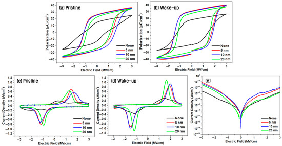
Figure 3.
P–E loops (a,b), switching current (c,d), and leakage current (e) of capacitors with a symmetric electrode structure annealed at 700 °C, as a function of the W insertion layer thickness; (a,c) in the pristine state and (b,d) in the wake-up state.
Figure 3c,d show the switching current measurements. In the absence of the W insertion layer, the switching current in the pristine state exhibited weak double peaks, whereas devices with W layers exhibited clearly defined switching peaks. After wake-up cycling, all devices exhibited enhanced ferroelectricity, and the switching current peak areas were largest in devices with 5–10 nm-thick W layers, consistent with the observed remnant polarization values.
As shown in Figure 3e, the leakage current increased by up to one order of magnitude in devices with W insertion layers. This increase is believed to result from the diffusion of W atoms into the HZO film during annealing, in which the presence of metallic ions in the oxide matrix reduces the insulation quality and thus increases the leakage current [24,25,26].
Figure 4 shows the XRD analysis results of HZO thin-films in the symmetric electrode structure from Figure 3 as a function of the W insertion layer thickness. XRD analysis was conducted over the 2θ range of 28–33°, and Gaussian deconvolution was applied around the o-phase (~30.5°) and t-phase (~30.8°) to fit the diffraction patterns. The relative ratio of o-/t-phase was determined by integrating the area under each fitted peak [27,28,29]. In the TiN/HZO/TiN structure without a W insertion layer, the o-phase fraction decreased from 62.6% at 600 °C to 59.1% at 700 °C, consistent with the general trend that higher annealing temperatures favor the thermodynamically stable t-phase and suppress o-phase formation [30,31,32]. By contrast, when the W insertion layer was used the o-phase fraction increased with increasing annealing temperature, regardless of the W layer thickness. This can be attributed to the greater TEC mismatch between the HZO and W (α = 4.4 × 10⁻⁶ K−1) compared to TiN, resulting in greater tensile stress that helps stabilize the o-phase [33,34]. Based on a simple calculation using Equation (1), the tensile strain induced by the TEC mismatch at the W/HZO and TiN/HZO interfaces under a 700 °C annealing condition is estimated to be approximately 0.38% and 0.04%, respectively. This difference may be significant in promoting the phase transformation into the metastable ferroelectric phase [35]. Notably, the o-phase fraction peaked at 81.1% when the W insertion layer was 5 nm-thick and remained high at 80.1% with a 10 nm-thick W layer. However, it decreased to 75% when a 20 nm-thick W insertion was used. This trend was consistent with the 2Pr values observed in the electrical measurements.
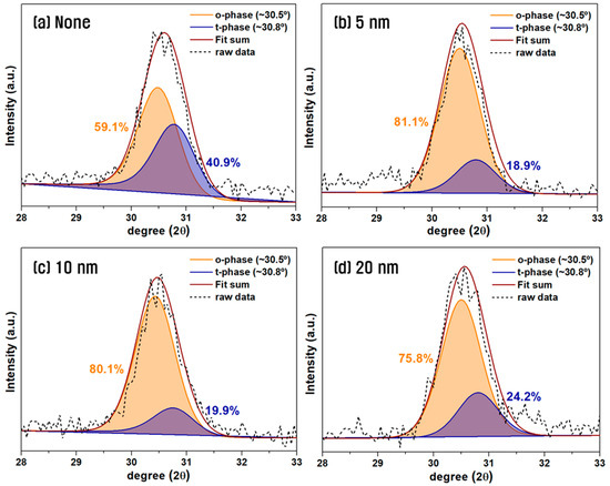
Figure 4.
XRD patterns of HZO films with different W insertion thicknesses after 700 °C RTA in a symmetric electrode structure.
Figure 5 presents the electrical characterization of capacitors with various electrode configurations, each using a 5 nm-thick W insertion layer. As shown in Figure 5a, comparing the pristine states, devices without a W layer, or with a W layer only at the top electrode, exhibited low 2Pr values and weak polarization curves. By contrast, configurations with the W layer at the bottom electrode, or at both the top and bottom, exhibited strong ferroelectric behavior with high 2Pr values.
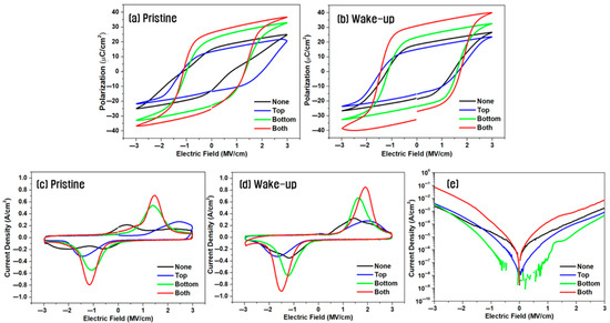
Figure 5.
P–E loops (a,b), switching current (c,d), and leakage current (e) of capacitors with various electrode configurations using 5 nm-thick W insertion layer; (a,c) in the pristine state and (b,d) in the wake-up state.
As shown in Figure 5b, the wake-up state measurements show well-formed ferroelectric hysteresis curves in all configurations. The dual W insertion structure (top and bottom) produced the highest 2Pr value of 61 μC/cm2. The asymmetric configuration with W only at the bottom yielded the second highest value of 47 μC/cm2, whereas placing W only at the top resulted in a lower 2Pr of 30.5 μC/cm2.
The switching current results shown in Figure 5c,d reinforce this trend. Devices without W, or with top-only W layers, exhibited weak, asymmetric switching current peaks in the pristine state. By contrast, devices with W at the bottom, or at both interfaces, exhibited distinct polarization current peaks. After wake-up, these devices exhibited larger peak areas and more symmetric switching currents, consistent with enhanced ferroelectric performance. Notably, in the device incorporating W electrodes on both sides, the positions of the two switching current peaks are shifted toward the positive and negative directions, respectively. The shift reflects an increase in the coercive field, implying that a higher electric field is required to induce polarization reversal. We know that W is a metal with excellent oxidation resistance and low reactivity at the HZO interface, effectively suppressing the formation of undesirable interfacial oxide layers [36,37,38]. In typical TiN/HZO structures, oxygen supplied during HZO deposition can react with the bottom TiN electrode to form TiOx interfacial layers, which can be expected to be thicker than those at the top interface. These interfacial oxides can alter the electron affinity and the intrinsic band structure at the interface. In particular, the conduction band minimum at the bottom interface can rise more than that at the top, increasing the conduction band offset (CBO). If this CBO becomes too large, it can concentrate the electric field at the interface, leading to the breakdown and degradation of electrical properties [39,40,41]. Consequently, inserting W at the bottom electrode can be expected to more effectively suppress interfacial oxide growth and stabilize the CBO, contributing more to device performance than top-only W insertion.
Figure 5e shows the leakage current results. The device with W only at the bottom electrode exhibited a lower leakage current compared to those with no W or top-only W insertion. The highest leakage current was evident in the dual-insertion device, likely owing to the excessive diffusion of W during high-temperature annealing.
Figure 6 shows the XRD analysis results of HZO films with the different electrode configurations described in Figure 5. When W was inserted only at the top electrode, the o-phase fraction was even lower than that of the device without any W insertion. By contrast, inserting W at the bottom electrode, or at both electrodes, increased the o-phase fraction to 74.8% and 81.1%, respectively. As in the previous results, a strong correlation was evident between the o-phase fraction and the 2Pr values measured in Figure 5, confirming a proportional relationship.
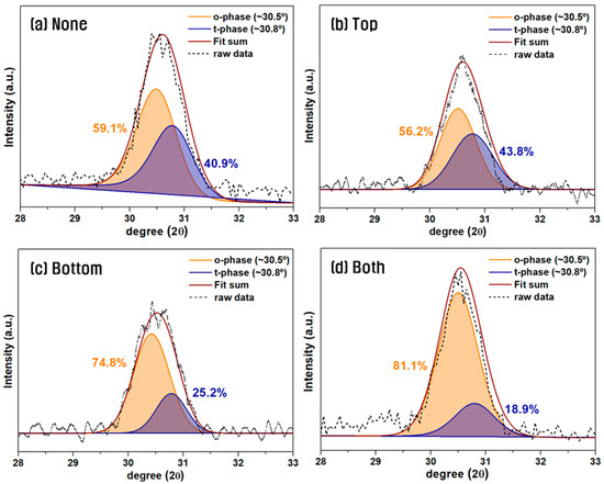
Figure 6.
XRD patterns of HZO films with four different electrode configurations using 5 nm-thick W insertion layer.
To analyze the cause of the crystallinity and electrical property variations depending on the W insertion position in the MFM device structure, XPS analysis was conducted. The XPS measurements were performed using a depth profiling method, in which the samples were etched 20 times after full device fabrication until reaching the bottom TiN electrode. Spectral analysis was based on the region within the HZO film where the relative concentration of Hf and Zr was the highest. Figure 7 shows the XPS narrow-scan spectra of Hf 4f and O 1s for the HZO films corresponding to the devices shown in Figure 5 and Figure 6, with different W insertion layer positions. In Figure 7a–d, the Hf 4f peaks were deconvoluted using a Gaussian fitting method with the intensity of 4f7/2:4f5/2 fixed at 4:3, a spin–orbit splitting of 1.66 eV, and identical FWHM constraints [42]. The proportion of non-stoichiometric HfO2−x—indicative of lattice defects in HfO2—was 26.8% in the sample without a W insertion layer, whereas with W inserted at the bottom, or at both interfaces, the ratio decreased to 20.9% and 13.9%, respectively.
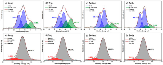
Figure 7.
Comparison of narrow-scan XPS spectra of (a–d) Hf 4f and (e–h) O 1s for different electrode configurations.
The O 1s peak narrow-scan analysis shown in Figure 7e–h was used to examine the proportion of non-lattice oxygen, which corresponds to oxygen vacancies in the HZO film. Although the non-lattice component may include various oxygen-related species such as O-H and C-O, in addition to oxygen vacancies, no distinct peaks corresponding to C–O (286.5 eV) or O–C=O (288.5 eV) were observed in the C 1s spectrum acquired at the same depth, thereby excluding the possibility of contamination from C–O-related species. Compared to the 8.02% non-lattice oxygen in the film without a W insertion layer, the ratios dropped to 6.95% and 5.93% when W was inserted at the bottom and both electrodes, respectively. These results indicate that placing the W insertion layer at the bottom, or at both interfaces, reduces the presence of non-stoichiometric Hf species and non-lattice oxygen components. This trend is consistent with the previously observed increase in 2Pr and the change in the o-/t-phase ratio. Therefore, the reduction in defect states is believed to have played a crucial role in the structural stability of the HZO film and the enhancement in the electrical performance of HZO-based capacitors [43,44,45,46].
In particular, when W was inserted only at the top electrode, the defect ratio increased, which supports the earlier interpretation that inserting W at the bottom electrode effectively suppresses interfacial oxide formation and stabilized the CBO, thereby having a more favorable impact on device performance. These findings suggest that applying the W insertion layer to the bottom electrode, rather than the top, may more significantly contribute to the structural and electrical enhancement of the device.
Figure 8 shows the high-resolution, cross-sectional TEM images and corresponding fast Fourier transform (FFT) patterns of the HZO thin-films with and without a W insertion layer. In both films, well-defined interfaces and sufficient crystallization could be observed; however, the interface between the HZO and TiN was smoother and more distinct when a W insertion layer was used. Regardless of the presence of W, the HZO films had similar thicknesses under identical ALD cycle conditions.
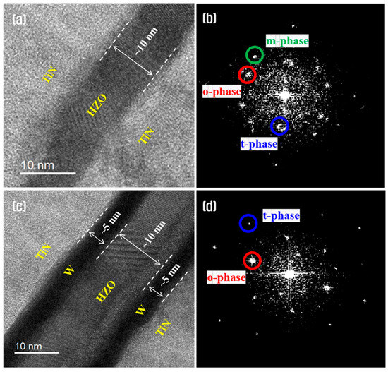
Figure 8.
Cross-sectional, high-resolution TEM images (a,c) and corresponding FFT patterns (b,d) of the HZO thin-films with and without a W insertion layer.
Figure 8b,d reveal that in the absence of a W insertion layer diffraction patterns corresponding to the m-phase (with a d-spacing of 3.16 Å) were evident in addition to the o-phase and t-phase peaks. By contrast, in the presence of a W insertion layer only the o-phase (2.65 Å) and t-phase (2.92 Å) patterns could be identified. This suggests that the W layer effectively suppressed interfacial reactions between HZO and TiN, promoted o-phase transition, and successfully inhibited undesirable m-phase formation [47,48].
Figure 9a shows the variation in the o-phase and t-phase fractions of all fabricated HZO capacitors as a function of their measured 2Pr values. As 2Pr increased, the o-phase fraction increased linearly, whereas the t-phase fraction decreased correspondingly. This confirms that an increased proportion of the metastable o-phase is the key to strong ferroelectric performance in HZO films [49,50,51].
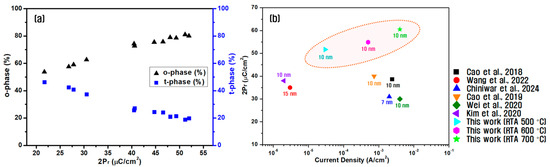
Figure 9.
(a) Variation in the o- and t-phase fractions of the fabricated HZO films as a function of 2Pr and (b) comparison of the electrical performance of the developed hybrid TiN/W/HZO/W/TiN capacitors with previously reported devices without a W insertion layer [10,37,46,52,53,54].
Figure 9b compares the electrical performance—specifically the polarization and leakage current—of the developed symmetric hybrid TiN/W/HZO/W/TiN capacitors with those of previously reported TiN/HZO/TiN or W/HZO/W capacitors without W insertion layers. Most reference devices were annealed at 500 °C, conditions under which the capacitor fabricated in this study exhibited the highest 2Pr value. Here, 2Pr increased with higher annealing temperatures. The leakage current values were also lower or comparable to other devices with similar HZO thickness, demonstrating that the use of a W insertion layer could simultaneously improve the polarization performance and suppress the leakage current.
4. Conclusions
In this study, HZO thin-films were deposited using a CPALD process that simultaneously used DP and RP. The influence of the thickness and position of W insertion layers in a symmetric hybrid electrode configuration on the electrical performance of CPALD HZO ferroelectric capacitors was investigated. Under 700 °C annealing conditions, the device with 5 nm-thick W insertion layers applied at both the top and bottom electrodes exhibited excellent ferroelectric properties, even before wake-up cycling. After wake-up the capacitor exhibited a remarkably high remnant polarization of 2Pr = 61.0 μC/cm2. The position of the W insertion layer clearly affected the device characteristics—for example, inserting W at the bottom electrode resulted in higher 2Pr values and a considerably reduced leakage current compared to top-only insertion. This improvement could be attributed to the large TEC mismatch between W and HZO, which generated tensile stress, and to the suppression of interfacial oxide layer formation caused by reactions between the bottom TiN electrode and oxygen during the deposition process. Overall, the W insertion layer contributed to improved electrical performance by stabilizing the o-phase within the HZO film and reducing the formation of interfacial defects. The CPALD technique and the optimization of hybrid electrode configurations using W insertion layers have demonstrated promising potential for enhancing the performance of ferroelectric capacitors. Furthermore, for such devices to be viable candidates for next-generation memory applications, it is essential to achieve high cycling endurance and long retention times. To this end, we are currently preparing follow-up studies focused on addressing these critical reliability metrics.
Author Contributions
Conceptualization, H.-C.L.; methodology, H.-J.K. and S.-W.K.; software, H.-J.K. and J.-H.C.; validation S.-W.K. and S.-E.L.; formal analysis, H.-J.K.; investigation, S.-W.K.; resources, H.-J.K. and J.-H.C.; data curation, S.-W.K.; writing—original draft preparation, H.-J.K. and J.-H.C.; writing—review and editing, H.-C.L.; visualization, S.-W.K.; supervision, S.-E.L.; project administration, H.-C.L.; funding acquisition, H.-C.L. All authors have read and agreed to the published version of the manuscript.
Funding
This work was supported by the Priority Research Centers Program grant through the National Research Foundation (NRF) of Korea, funded by the Ministry of Education (Grant No. 2017R1A6A1A03015562) and by the Korea Collaborative & High-tech Initiative for Prospective Semiconductor Research (K-CHIPS) funded by the Ministry of Trade, Industry & Energy (MOTIE, Republic of Korea) (Grant Numbers 1415187710, RS-2023-00237030, and 23027-15FC).
Institutional Review Board Statement
Not applicable.
Informed Consent Statement
Not applicable.
Data Availability Statement
The original contributions presented in this study are included in the article. Further inquiries can be directed to the corresponding authors.
Conflicts of Interest
The authors declare no conflicts of interest.
Abbreviations
The following abbreviations are used in this manuscript:
| ALD | Atomic layer deposition |
| CBO | Conduction band offset |
| CPALD | Co-plasma atomic layer deposition |
| DP | Direct plasma |
| FE-TEM | Field emission transmission electron microscopy |
| FFT | Fast Fourier transform |
| MFM | Metal–ferroelectric–metal |
| PEALD | Plasma-enhanced atomic layer deposition |
| RP | Remote plasma |
| RPS | Remote plasma system |
| RTA | Rapid thermal annealing |
| TEC | Thermal expansion coefficient |
| TEM | Transmission electron microscopy |
| XPS | X-ray photoelectron spectroscopy |
| XRD | X-ray diffraction |
References
- Cho, D.Y.; Jung, H.S.; Yu, I.H.; Yoon, J.H.; Kim, H.K.; Lee, S.Y.; Jeon, S.H.; Han, S.; Kim, J.H.; Park, T.J.; et al. Stabilization of Tetragonal HfO2 under Low Active Oxygen Source Environment in Atomic Layer Deposition. Chem. Mater. 2012, 24, 3534–3543. [Google Scholar] [CrossRef]
- Salahuddin, S.; Ni, K.; Datta, S. The Era of Hyper-Scaling in Electronics. Nat. Electron. 2018, 1, 442–450. [Google Scholar] [CrossRef]
- Borg, M.; Papadopoulos, C.; Yu, S.; Hur, J.; Luo, Y.; Shim, W.; Choe, G. Ferroelectric HfO2-Based Synaptic Devices: Recent Trends and Prospects. Semicond. Sci. Technol. 2021, 36, 104001. [Google Scholar] [CrossRef]
- Chen, G.H.; Chen, Y.R.; Zhao, Z.; Lee, J.Y.; Chen, Y.W.; Xing, Y.; Dobhal, R.; Liu, C.W. A Kinetic Pathway to Orthorhombic HfZrO. IEEE J. Electron Devices Soc. 2023, 11, 752–758. [Google Scholar] [CrossRef]
- Mueller, S.; Mueller, J.; Singh, A.; Riedel, S.; Sundqvist, J.; Schroeder, U.; Mikolajick, T. Incipient Ferroelectricity in Al-Doped HfO2 Thin Films. Adv. Funct. Mater. 2012, 22, 2412–2417. [Google Scholar] [CrossRef]
- Martin, D.; Müller, J.; Schenk, T.; Arruda, T.M.; Kumar, A.; Strelcov, E.; Yurchuk, E.; Müller, S.; Pohl, D.; Schröder, U.; et al. Ferroelectricity in Si-Doped HfO2 Revealed: A Binary Lead-Free Ferroelectric. Adv. Mater. 2014, 26, 8198–8202. [Google Scholar] [CrossRef] [PubMed]
- Huang, F.; Wang, Y.; Liang, X.; Qin, J.; Zhang, Y.; Yuan, X.; Wang, Z.; Peng, B.; Deng, L.; Liu, Q.; et al. HfO2-Based Highly Stable Radiation-Immune Ferroelectric Memory. IEEE Electron Device Lett. 2017, 38, 330–333. [Google Scholar] [CrossRef]
- Kobayashi, M.; Wu, J.; Sawabe, Y.; Takuya, S.; Hiramoto, T. Mesoscopic-Scale Grain Formation in HfO2-Based Ferroelectric Thin Films and Its Impact on Electrical Characteristics. Nano Converg. 2022, 9, 50. [Google Scholar] [CrossRef] [PubMed]
- Park, W.J.; Kim, H.J.; Lee, J.H.; Kim, J.H.; Uhm, S.H.; Kim, S.W.; Lee, H.C. Characterization of HZO Films Fabricated by Co-Plasma Atomic Layer Deposition for Ferroelectric Memory Applications. Nanomaterials 2024, 14, 1801. [Google Scholar] [CrossRef]
- Cao, R.; Wang, Y.; Zhao, S.; Yang, Y.; Zhao, X.; Wang, W.; Zhang, X.; Lv, H.; Liu, Q.; Liu, M. Effects of Capping Electrode on Ferroelectric Properties of Hf0.5Zr0.5O2 Thin Films. IEEE Electron Device Lett. 2018, 39, 1207–1210. [Google Scholar] [CrossRef]
- Kim, S.J.; Mohan, J.; Summerfelt, S.R.; Kim, J. Ferroelectric Hf0.5Zr0.5O2 Thin Films: A Review of Recent Advances. Jom 2019, 71, 246–255. [Google Scholar] [CrossRef]
- Wang, C.I.; Wang, C.Y.; Chang, T.J.; Jiang, Y.S.; Shyue, J.J.; Lin, H.C.; Chen, M.J. Atomic Layer Deposited TiN Capping Layer for Sub-10 nm Ferroelectric Hf0.5Zr0.5O2 with Large Remnant Polarization and Low Thermal Budget. Appl. Surf. Sci. 2021, 570, 151152. [Google Scholar] [CrossRef]
- Chen, Y.F.; Wang, C.H.; Shih, H.Y.; Kuo, C.Y.; Wu, Y.H. Polarization and Reliability Enhancement for Ferroelectric Capacitors by Interface Engineering Through Crystalline TaN. IEEE Trans. Electron Devices 2024, 71, 3433–3438. [Google Scholar] [CrossRef]
- Zhang, J.; Yu, J.; Li, Z.; Xu, K.; Liu, Y.; Meng, J.; Zhu, H.; Sun, Q.; Zhu, X.; Zhang, D.W.; et al. Excellent Reliability in Hf0.5Zr0.5O2based Ferroelectric Device with Oxygen-Doped ITO Electrodes. IEEE Electron Device Lett. 2024, 45, 2565–2568. [Google Scholar] [CrossRef]
- Hsiang, K.Y.; Liao, C.Y.; Lin, Y.Y.; Lou, Z.F.; Lin, C.Y.; Lee, J.Y.; Chang, F.S.; Li, Z.X.; Tseng, H.C.; Wang, C.C.; et al. Correlation between Access Polarization and High Endurance (~1012 cycling) of Ferroelectric and Anti-Ferroelectric HfZrO2. In Proceedings of the 2022 IEEE International Reliability Physics Symposium (IRPS), Dallas, TX, USA, 27–31 March 2022; pp. P91–P94. [Google Scholar] [CrossRef]
- Koroleva, A.A.; Chernikova, A.G.; Zarubin, S.S.; Korostylev, E.; Khakimov, R.R.; Zhuk, M.Y.; Markeev, A.M. Retention Improvement of HZO-Based Ferroelectric Capacitors with TiO2 Insets. ACS Omega 2022, 7, 47084–47095. [Google Scholar] [CrossRef]
- Park, M.H.; Lee, Y.H.; Kim, H.J.; Kim, Y.J.; Moon, T.; Do Kim, K.; Hyun, S.D.; Mikolajick, T.; Schroeder, U.; Hwang, C.S. Understanding the Formation of the Metastable Ferroelectric Phase in Hafnia-Zirconia Solid Solution Thin Films. Nanoscale 2018, 10, 716–725. [Google Scholar] [CrossRef]
- Kim, H.J.; Park, M.H.; Kim, Y.J.; Lee, Y.H.; Moon, T.; Do Kim, K.; Hyun, S.D.; Hwang, C.S. A Study on the Wake-up Effect of Ferroelectric Hf0.5Zr0.5O2 Films by Pulse-Switching Measurement. Nanoscale 2016, 8, 1383–1389. [Google Scholar] [CrossRef]
- Kim, B.S.; Hyun, S.D.; Moon, T.; Do Kim, K.; Lee, Y.H.; Park, H.W.; Lee, Y.B.; Roh, J.; Kim, B.Y.; Kim, H.H.; et al. A Comparative Study on the Ferroelectric Performances in Atomic Layer Deposited Hf0.5Zr0.5O2 Thin Films Using Tetrakis(Ethylmethylamino) and Tetrakis(Dimethylamino) Precursors. Nanoscale Res. Lett. 2020, 15, 72. [Google Scholar] [CrossRef]
- Choi, Y.; Han, C.; Shin, J.; Moon, S.; Min, J.; Park, H.; Eom, D.; Lee, J.; Shin, C. Impact of Chamber/Annealing Temperature on the Endurance Characteristic of Zr:HfO2 Ferroelectric Capacitor. Sensors 2022, 22, 4087. [Google Scholar] [CrossRef]
- Cheng, X.; Zhou, C.; Lin, B.; Yang, Z.; Chen, S.; Zhang, K.H.L.; Chen, Z. Leakage Mechanism in Ferroelectric Hf0.5Zr0.5O2 Epitaxial Thin Films. Appl. Mater. Today 2023, 32, 101804. [Google Scholar] [CrossRef]
- Yang, K.; Jeong, H.W.; Lee, J.; Cho, Y.H.; Park, J.Y.; Choi, H.; Kim, Y.Y.; Lee, Y.; Kim, Y.; Park, M.H. Texture Modulation of Ferroelectric Hf0.5Zr0.5O2 Thin Films by Engineering the Polymorphism and Texture of Tungsten Electrodes. J. Mater. 2025, 11, 101015. [Google Scholar] [CrossRef]
- Lee, S.J.; Kim, T.H.; Jeong, B.H.; Kim, K.N.; Yeom, G.Y. Properties of Tungsten Thin Film Deposited Using Inductively Coupled Plasma Assisted Sputtering for Next-Generation Interconnect Metal. Thin Solid Film. 2019, 674, 64–70. [Google Scholar] [CrossRef]
- Mannequin, C.; Gonon, P.; Vallée, C.; Latu-Romain, L.; Bsiesy, A.; Grampeix, H.; Salaün, A.; Jousseaume, V. Stress-Induced Leakage Current and Trap Generation in HfO2 Thin Films. J. Appl. Phys. 2012, 112, 074103. [Google Scholar] [CrossRef]
- Ranjan, A.; Xu, H.; Wang, C.; Molina, J.; Wu, X.; Zhang, H.; Sun, L.; Chu, J.; Pey, K.L. Probing Resistive Switching in HfO2/Al2O3 Bilayer Oxides Using in-Situ Transmission Electron Microscopy. Appl. Mater. Today 2023, 31, 101739. [Google Scholar] [CrossRef]
- Wang, X.; Wu, M.; Zhang, T.; Cui, B.; Li, Y.C.; Liu, J.; Wu, Y.; Wen, Y.; Ye, S.; Ren, P.; et al. Exploring tungsten-oxygen vacancy synergy: Impact on leakage characteristics in Hf0.5Zr0.5O2 ferroelectric thin films. Appl. Phys. Lett. 2024, 124, 232901. [Google Scholar] [CrossRef]
- Gaddam, V.; Das, D.; Jeon, S. Insertion of HfO2 Seed/Dielectric Layer to the Ferroelectric HZO Films for Heightened Remanent Polarization in MFM Capacitors. IEEE Trans. Electron Devices 2020, 67, 745–750. [Google Scholar] [CrossRef]
- Zhou, J.; Zhou, Z.; Jiao, L.; Wang, X.; Kang, Y.; Wang, H.; Han, K.; Zheng, Z.; Gong, X. Al-Doped and Deposition Temperature-Engineered HfO2 Near Morphotropic Phase Boundary with Record Dielectric Permittivity (68). In Proceedings of the 2021 IEEE International Electron Devices Meeting (IEDM), San Francisco, CA, USA, 11–16 December 2021; pp. 13.4.1–13.4.4. [Google Scholar] [CrossRef]
- Kashir, A.; Hwang, H. Ferroelectric and Dielectric Properties of Hf0.5Zr0.5O2 Thin Film Near Morphotropic Phase Boundary. Phys. Status Solidi Appl. Mater. Sci. 2021, 218, 2000819. [Google Scholar] [CrossRef]
- Hsain, H.A.; Lee, Y.; Parsons, G.; Jones, J.L. Compositional Dependence of Crystallization Temperatures and Phase Evolution in Hafnia-Zirconia (HfxZr1−x)O2thin Films. Appl. Phys. Lett. 2020, 116, 192901. [Google Scholar] [CrossRef]
- Yu, G.T.; Park, G.H.; Lee, E.B.; Park, M.H. Review of the Mechanism for Ferroelectric Phase Formation in Fluorite-Structure Oxide. New Phys. Sae Mulli 2021, 71, 890–900. [Google Scholar] [CrossRef]
- Hyuk Park, M.; Joon Kim, H.; Jin Kim, Y.; Lee, W.; Moon, T.; Seong Hwang, C. Evolution of Phases and Ferroelectric Properties of Thin Hf0.5Zr0.5O2 Films According to the Thickness and Annealing Temperature. Appl. Phys. Lett. 2013, 102, 242905. [Google Scholar] [CrossRef]
- Hwang, C.S. Prospective of Semiconductor Memory Devices: From Memory System to Materials. Adv. Electron. Mater. 2015, 1, 1400056. [Google Scholar] [CrossRef]
- Kashir, A.; Kim, H.; Oh, S.; Hwang, H. Large Remnant Polarization in a Wake-Up Free Hf0.5Zr0.5O2 Ferroelectric Film through Bulk and Interface Engineering. ACS Appl. Electron. Mater. 2021, 3, 629–638. [Google Scholar] [CrossRef]
- Park, M.H.; Schenk, T.; Fancher, C.M.; Grimley, E.D.; Zhou, C.; Richter, C.; Lebeau, J.M.; Jones, J.L.; Mikolajick, T.; Schroeder, U. A Comprehensive Study on the Structural Evolution of HfO2 Thin Films Doped with Various Dopants. J. Mater. Chem. C 2017, 5, 4677–4690. [Google Scholar] [CrossRef]
- Lin, Y.J.; Teng, C.Y.; Chang, S.J.; Liao, Y.F.; Hu, C.; Su, C.J.; Tseng, Y.C. Role of Electrode-Induced Oxygen Vacancies in Regulating Polarization Wake-up in Ferroelectric Capacitors. Appl. Surf. Sci. 2020, 528, 147014. [Google Scholar] [CrossRef]
- Wang, D.; Zhang, Y.; Wang, J.; Luo, C.; Li, M.; Shuai, W.; Tao, R.; Fan, Z.; Chen, D.; Zeng, M.; et al. Enhanced Ferroelectric Polarization with Less Wake-up Effect and Improved Endurance of Hf0.5Zr0.5O2 Thin Films by Implementing W Electrode. J. Mater. Sci. Technol. 2022, 104, 1–7. [Google Scholar] [CrossRef]
- Yang, K.; Kim, G.Y.; Ryu, J.J.; Lee, D.H.; Park, J.Y.; Kim, S.H.; Park, G.H.; Yu, G.T.; Kim, G.H.; Choi, S.Y.; et al. Wake-up-Mitigated Giant Ferroelectricity in Hf0.5Zr0.5O2 Thin Films through Oxygen-Providing, Surface-Oxidized W Electrode. Mater. Sci. Semicond. Process. 2023, 164, 107565. [Google Scholar] [CrossRef]
- Matveyev, Y.; Negrov, D.; Chernikova, A.; Lebedinskii, Y.; Kirtaev, R.; Zarubin, S.; Suvorova, E.; Gloskovskii, A.; Zenkevich, A. Effect of Polarization Reversal in Ferroelectric TiN/Hf0.5Zr0.5O2/TiN Devices on Electronic Conditions at Interfaces Studied in Operando by Hard X-Ray Photoemission Spectroscopy. ACS Appl. Mater. Interfaces 2017, 9, 43370–43376. [Google Scholar] [CrossRef]
- Mu, X.; Wu, Y.; Zeng, B.; Jiang, J.; Zhou, Y.; Yin, L.; Liao, M.; Yang, Q. Polarization Switching of HfO2 Ferroelectric in Bulk and Electrode/Ferroelectric/Electrode Heterostructure. npj Comput. Mater. 2025, 11, 126. [Google Scholar] [CrossRef]
- Ambriz-Vargas, F.; Kolhatkar, G.; Broyer, M.; Hadj-Youssef, A.; Nouar, R.; Sarkissian, A.; Thomas, R.; Gomez-Yáñez, C.; Gauthier, M.A.; Ruediger, A. A Complementary Metal Oxide Semiconductor Process-Compatible Ferroelectric Tunnel Junction. ACS Appl. Mater. Interfaces 2017, 9, 13262–13268. [Google Scholar] [CrossRef]
- Major, G.H.; Fairley, N.; Sherwood, P.M.A.; Linford, M.R.; Terry, J.; Fernandez, V.; Artyushkova, K. Practical Guide for Curve Fitting in X-Ray Photoelectron Spectroscopy. J. Vac. Sci. Technol. A 2020, 38, 061203. [Google Scholar] [CrossRef]
- Pešić, M.; Fengler, F.P.G.; Larcher, L.; Padovani, A.; Schenk, T.; Grimley, E.D.; Sang, X.; LeBeau, J.M.; Slesazeck, S.; Schroeder, U.; et al. Physical Mechanisms behind the Field-Cycling Behavior of HfO2-Based Ferroelectric Capacitors. Adv. Funct. Mater. 2016, 26, 4601–4612. [Google Scholar] [CrossRef]
- Lee, Y.; Goh, Y.; Hwang, J.; Das, D.; Jeon, S. The Influence of Top and Bottom Metal Electrodes on Ferroelectricity of Hafnia. IEEE Trans. Electron Devices 2021, 68, 523–528. [Google Scholar] [CrossRef]
- Goh, Y.; Cho, S.H.; Park, S.H.K.; Jeon, S. Oxygen Vacancy Control as a Strategy to Achieve Highly Reliable Hafnia Ferroelectrics Using Oxide Electrode. Nanoscale 2020, 12, 9024–9031. [Google Scholar] [CrossRef]
- Chiniwar, S.P.; Hsieh, Y.C.; Shih, C.H.; Teng, C.Y.; Yang, J.L.; Hu, C.; Lin, B.H.; Tang, M.T.; Tseng, Y.C. Ferroelectric Enhancement in a TiN/Hf1−XZrxO2/W Device with Controlled Oxidation of the Bottom Electrode. ACS Appl. Electron. Mater. 2024, 6, 1078–1086. [Google Scholar] [CrossRef]
- Kim, S.J.; Narayan, D.; Lee, J.G.; Mohan, J.; Lee, J.S.; Lee, J.; Kim, H.S.; Byun, Y.C.; Lucero, A.T.; Young, C.D.; et al. Large Ferroelectric Polarization of TiN/Hf0.5Zr0.5O2/TiN Capacitors Due to Stress-Induced Crystallization at Low Thermal Budget. Appl. Phys. Lett. 2017, 111, 242901. [Google Scholar] [CrossRef]
- Dai, S.; Yang, C.; Wang, Y.; Jiang, Y.; Zeng, L. In Situ TEM Studies of Tunnel-Structured Materials for Alkali Metal-Ion Batteries. Adv. Sci. 2025, 12, 2500513. [Google Scholar] [CrossRef]
- Lederer, M.; Olivo, R.; Lehninger, D.; Abdulazhanov, S.; Kämpfe, T.; Kirbach, S.; Mart, C.; Seidel, K.; Eng, L.M. On the Origin of Wake-Up and Antiferroelectric-Like Behavior in Ferroelectric Hafnium Oxide. Phys. Status Solidi-Rapid Res. Lett. 2021, 15, 2100086. [Google Scholar] [CrossRef]
- Fan, Y.; Zhang, S.; Xue, Z.; Dong, Y.; Chen, D.; Zhang, J.; Liu, J.; Si, M.; Luo, C.; Li, W.; et al. Hidden Structural Phase Transition Assisted Ferroelectric Domain Orientation Engineering in Hf0.5Zr0.5O2 Films. Nat. Commun. 2025, 16, 4232. [Google Scholar] [CrossRef]
- Cho, H.W.; Pujar, P.; Choi, M.; Kang, S.; Hong, S.; Park, J.; Baek, S.; Kim, Y.; Lee, J.; Kim, S. Direct Growth of Orthorhombic Hf0.5Zr0.5O2 Thin Films for Hysteresis-Free MoS2 Negative Capacitance Field-Effect Transistors. npj 2D Mater. Appl. 2021, 5, 46. [Google Scholar] [CrossRef]
- Cao, R.; Liu, Q.; Liu, M.; Song, B.; Shang, D.; Yang, Y.; Luo, Q.; Wu, S.; Li, Y.; Wang, Y.; et al. Improvement of Endurance in HZO-Based Ferroelectric Capacitor Using Ru Electrode. IEEE Electron Device Lett. 2019, 40, 1744–1747. [Google Scholar] [CrossRef]
- Wei, W.; Zhang, W.; Wang, F.; Ma, X.; Wang, Q.; Sang, P.; Zhan, X.; Li, Y.; Tai, L.; Luo, Q.; et al. Deep Insights into the Failure Mechanisms in Field-Cycled Ferroelectric Hf0.5Zr0.5O2 Thin Film: TDDB Characterizations and First-Principles Calculations. In Proceedings of the 2020 IEEE International Electron Devices Meeting (IEDM), San Francisco, CA, USA, 12–18 December 2020; pp. 39.6.1–39.6.4. [Google Scholar] [CrossRef]
- Kim, H.; Kashir, A.; Oh, S.; Hwang, H. A New Approach to Achieving Strong Ferroelectric Properties in TiN/Hf0.5Zr0.5O2/TiN Devices. Nanotechnology 2020, 32, 055703. [Google Scholar] [CrossRef] [PubMed]
Disclaimer/Publisher’s Note: The statements, opinions and data contained in all publications are solely those of the individual author(s) and contributor(s) and not of MDPI and/or the editor(s). MDPI and/or the editor(s) disclaim responsibility for any injury to people or property resulting from any ideas, methods, instructions or products referred to in the content. |
© 2025 by the authors. Licensee MDPI, Basel, Switzerland. This article is an open access article distributed under the terms and conditions of the Creative Commons Attribution (CC BY) license (https://creativecommons.org/licenses/by/4.0/).