Article

Stoichiometry of Bulk Nb1−βSnβ Superconductors Synthesised by Arc Melting

by
Mahboobeh Shahbazi
1,2,
Henrietta E. Cathey
3,
Ali Dehghan Manshadi
4,
Jose Alarco
1,2 and
Ian D. R. Mackinnon
2,3,*
1
Centre for Materials Science and School of Chemistry and Physics, Queensland University of Technology (QUT), Brisbane, QLD 4001, Australia
2
Centre for Clean Energy Technologies and Practices, Queensland University of Technology (QUT), Brisbane, QLD 4001, Australia
3
School of Earth and Atmospheric Sciences, Queensland University of Technology (QUT), Brisbane, QLD 4001, Australia
4
School of Mechanical and Mining Engineering, The University of Queensland, Brisbane, QLD 4072, Australia
*
Author to whom correspondence should be addressed.
Materials 2025, 18(13), 3050; https://doi.org/10.3390/ma18133050 (registering DOI)
Submission received: 23 May 2025 / Revised: 22 June 2025 / Accepted: 25 June 2025 / Published: 27 June 2025

Abstract

We present an alternative process for production of binary Nb1−βSnβ superconducting phases using pre- and post-treatment of arc-melted Nb + Sn ingots. This process combines sequential sintering, arc melting, and annealing procedures that provide dense, bulk samples of Nb1−βSnβ with varying stoichiometry between 0.18 < β < 0.25 depending on annealing time and temperature. We show, through magnetization measurements of these Nb1−βSnβ bulks, that annealing of arc-melted samples at 900 °C for 3 h significantly enhances Jc values compared with arc-melted Nb1−βSnβ samples without annealing. Microstructural analyses show that optimum grain size and orientation are achieved by sintering and annealing at lower temperatures (i.e., 720 °C and 900 °C, respectively) with short annealing times (i.e., <10 h). Processing at higher temperatures and for longer times enhances grain growth and results in fewer pinning centres. The optimum process creates effective pinning centres that deliver a Jc = 6.16 × 10⁴ A/cm2 at 10 K (and ~0.2 T), compared with Jc = 3.4 × 10⁴ A/cm2 for Nb1−βSnβ subjected to a longer annealing time at a higher temperature and Jc = 775 A/cm2 for an arc-melted sample without post-annealing. We suggest that further work addressing post-treatment annealing times between 3 h < tpost < 60 h at temperatures between 900 °C and 1000 °C will provide the opportunity to control stoichiometric and microstructural imperfections in bulk Nb1−βSnβ materials.

1. Introduction

Nb3Sn was discovered more than half a century ago [1] and continues to hold a crucial role in applications involving high-field magnets. These applications include nuclear magnetic resonance spectroscopy [2], future circular colliders [3], and the International Thermonuclear Experimental Reactor (ITER) [4]. Nb3Sn is an intermetallic compound of niobium and tin with an A15-type structure that enables superconductivity without anisotropy in wire applications [5]. Compared with common low-temperature superconducting materials, Nb3Sn has a higher Jc and higher Tc, but it is very brittle compared with ductile NbTi material [6].
The primary use of Nb3Sn is as superconducting wires for high-magnetic-field applications [7]. Effective application has built upon fundamental studies [5,8] of the binary Nb–Sn system and recognition that wire manufacture requires utilization of a ternary system such as Nb–Cu–Sn or Nb–Ti–Sn [5,7,9,10,11]. For example, the bronze route to synthesis using Cu enables production of Nb1−βSnβ compositions (including Nb3Sn) by moderating the chemical potential of component elements, particularly that of Sn [12]. An excellent summary of the reaction behaviors of Nb3Sn in wire processing via the bronze route and by other techniques is provided by Banno [12].
The synthesis of binary Nb3Sn as bulk material is a challenge due to the high diffusivity of Sn and other phases such as NbSn2, with consequent departure from Fick’s law [12]. These challenges led Devantay et al. [8], Goldacker et al. [13], and others to explore novel syntheses to produce homogeneous bulk Nb3Sn, for example, by using levitation melting at high Argon pressure [8] or by utilizing a hot isostatic press (HIP) at 1100 °C [13]. To further minimize inhomogeneity, Zhou et al. [14] also employed an HIP process capable of reaching temperatures up to 2200 °C in combination with ball milling and pre-annealing of starting materials.
Arc melting is an alternative synthesis technique to prepare metals, alloys, or intermetallics in bulk amounts with minimal contamination or introduction of impurities [15]. The process offers rapid in situ melting to very high temperatures, rapid solidification with minimal element losses, and uniform distribution of constituents [15]. The technique is readily available for laboratory use and is a well-established, scalable industrial process for many alloys and intermetallics [15]. For example, arc melting is used in steel manufacture [16,17], and for production of biomedical titanium alloys [18] and composite materials [19,20].
In this work, we evaluate pre-treatment preparation, arc melting of pre-treated samples, and annealing times before and after arc melting to explore their suitability for effective binary production of bulk Nb3Sn material. To determine the stoichiometry of specific phases in these bulk samples, we used high spatial and analytical precision electron microprobe analyses in addition to spatially resolved crystallographic parameters that enabled sub-micrometer delineation of the microstructure and phase relations. This work focuses on approaches amenable to bulk formation, while aiming for high homogeneity of the microstructure in order to expand the scope of potential applications for shaped Nb3Sn.

2. Materials and Methods

A molar ratio of niobium powder (45 μm, 99.8% purity) and tin powder (<325 mesh size, 99.8% purity) supplied by Sigma-Aldrich (Ryde, NSW, Australia) was weighed, ground in an agate mortar in an Argon-filled glove box, and pressed into a pellet (diameter ~1 cm × depth 5 mm) under an applied pressure of 10 tonne for 2 min. Since the difference in the melting temperature of Sn and Nb is large, arc melting may cause deviations from the intended stoichiometry due to vaporization or loss of Sn. Therefore, pre-annealing was performed on all samples to reduce the potential for Sn evaporation.
The pellet(s) for pre-annealing were placed inside a boron nitride sleeve within a 100 mL Parr reactor using a controlled atmosphere glove box containing Argon (99.99% purity). The reactor was then sealed tightly and removed from the glove box for operation. Two sets of samples were prepared using a mixture of 3:1 stoichiometric Nb + Sn, for heat treatment under an Ar atmosphere at a heating rate of 2 °C/minute to (i) 720 °C held for 105 h and (ii) to 1000 °C held for 60 h. The reactor temperature was thermocouple-controlled to ±2 °C.
These sintered pellets were then melted in an arc furnace on a water-cooled copper hearth under argon. The use of a water-cooled hearth with the arc melting technique helped reduce contamination from the crucible that contained the starting mixture and allowed easy removal of oxygen from the surrounding gas in the arc furnace. Prior to the arc-melting experiments, the chamber was vented and filled with argon three times and then filled with argon in order to eliminate oxygen in the chamber. The argon atmosphere was further purified by melting zirconium foam before melting the Nb-Sn pellet. The sample mixture was melted three times to ensure complete mixing. The arc-melted samples (diameter ~1 cm × 5 mm depth) were then annealed at 900 °C for 3 h; the second set of samples was annealed at 1000 °C for 60 h. All samples were subjected to the same annealing process (except for the time and temperature conditions) as described above for the pre-annealing process. Table 1 lists the sample IDs and relevant sintering and/or annealing time/temperature of the samples. After synthesis, ingots were split into representative pieces to enable phase, microstructural, and physical properties analyses.
All samples were subjected to x-ray powder diffraction (XRD) analysis using a Bruker D8 Advance X-ray diffractometer (Billerica, MA, USA) with Co Kα1 radiation in Bragg Brentano geometry. XRD measurements were performed with a step size of 0.02° 2θ and a counting time of 10 s per step. Diffraction patterns were refined and indexed using the software program Topas Version 6. Rietveld refinements using Topas determine quantitative estimates of phase abundance in each product. In general, phase abundances determined by this technique are within <5% relative error.
The microstructures of sintered, arc-melted, and annealed specimens were examined using scanning electron microscopy (SEM) equipped with microanalysis. Microstructural features were examined on polished samples using a field emission JEOL 7001SEM (JEOL Australasia Pty Ltd., French’s Forest, Australia), equipped with a secondary X-ray detector (Oxford Instruments SDD XMax 50 mm2, Abington, UK) and an electron backscatter diffraction (EBSD) pattern analyzer with Channel 5 analysis software and automated feature detection. Finely polished samples mounted in conductive resin were selected for EBSD mapping using an accelerating voltage of 25 kV and a step size of 0.2 µm.
Quantitative elemental analyses were performed using a JEOL JXA 8530F field emission electron probe microanalyzer (FE-EPMA, JEOL, Tokyo, Japan) equipped with five wavelength-dispersive spectrometers (WDS) and Probe for EPMA Version 13.9.1 software (Eugene, OR, USA). Operating conditions were 10 kV accelerating voltage with a beam current of 40 nA and a fully focused beam. Wavelength-dispersive analyzing crystals were PETL for Nb Lα and PETH for Sn Lα, and calibration standards included pure Nb and Sn metals. On- and off-peak counting times were 30 s, and a linear off-peak correction method was employed for background positions selected on either side of the analytical peaks.
Average detection limits (single spot, 3-sigma) were 360 ppm for Nb and 390 ppm for Sn, with relative analytical sensitivity (at the 99% confidence interval) of 0.3%. Estimated spatial resolution for each analysis under the EPMA operating conditions was ≤0.8 μm, based on Monte Carlo simulations of characteristic X-ray generation volumes in Nb3Sn (using density = 8.7) with CASINO Version 2.42 software [21]. For these analyses, the samples were combined with conductive resin and positioned in a 30 mm diameter mould within a hot mounting press. The mounted samples were then polished using a sequence of diamond pads and cloths to achieve a mirror-like finish, ideal for electron microprobe analysis.
Zero-field-cooled (ZFC) and field-cooled (FC) magnetization (M) curves were recorded as a function of temperature at 10 Oe using a Cryogenic Ltd. Mini Cryogen-free System (Cryogenic Ltd., London, UK). The system consisted of the following:
  • A pulse tube cryocooler with base temperature below 3 K and cooling power 0.5–1 W at 4.2 K;
  • A high-stability 20 bit magnet power supply;
  • A 5 Tesla magnet;
  • A variable temperature sample space of 25 mm ID, 100 mm long isothermal region;
  • A cryocooler for both the magnet and the sample space so that neither liquid nitrogen nor liquid helium was required.
Values for Tc were determined by finding the intersection of the linearly extrapolated M(T) with a constant M line. Magnetic hysteresis loops were measured at several temperatures below Tc for all samples. A magnetic Jc was calculated for samples using the Bean model: Jc = 20 ΔM/[a(1 − a/3b)] (a < b), where a and b are the width and length of the sample (in cm) perpendicular to the applied field, respectively. ΔM (in emu/cm3) is the width of the magnetic hysteresis loop and represents the difference in magnetization between the increasing and decreasing branches of the applied magnetic field and provides a value for Jc in A/cm2. Polichetti et al. [22] provide valuable discussion of the proper and improper use of formulae relevant to the Bean model. The formula used in this work followed that described as case study III in Table 3 of reference [22].

3. Results

Table 1 summarizes information regarding selected sample IDs, synthesis techniques, and heat-treatment conditions for the Nb3Sn bulks reported in this study. For instance, the sample ID “NS-1000/60” represents a Nb + Sn mixture sintered at 1000 °C for 60 h with no arc-melting process, while the ID “NS-1000/60/arc” represents a sample that has been subject to arc melting after a sintering process at 1000 °C for 60 h.
Two sintering temperatures, at 720 °C and 1000 °C, are evaluated in this work to explore the effects of both lower and higher sintering temperature. Preliminary evaluation showed that a Nb–Sn phase did not form with sintering at 720 °C. Nevertheless, NS-720/105/arc/ann/900/3 was prepared from an arc-melted sample where Nb + Sn mixtures were sintered at 720 °C for 105 h before arc melting, followed by annealing at 900 °C for 3 h. The sample ID NS-1000/60/arc/ann/1000/60 represents a sintered sample at 1000 °C for 60 h followed by arc melting and annealing treatment at 1000 °C for 60 h.

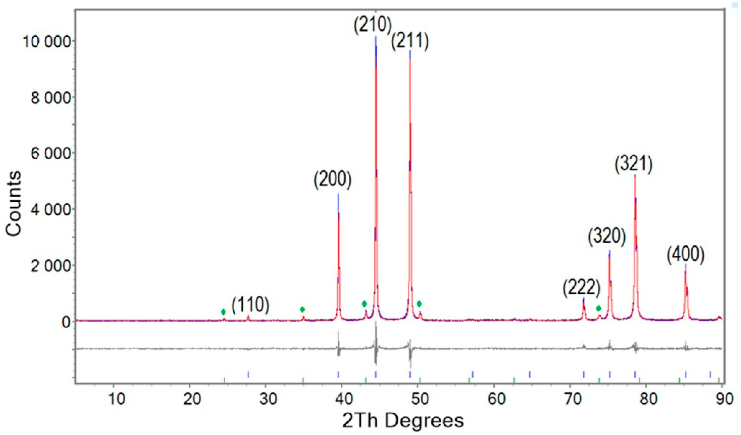
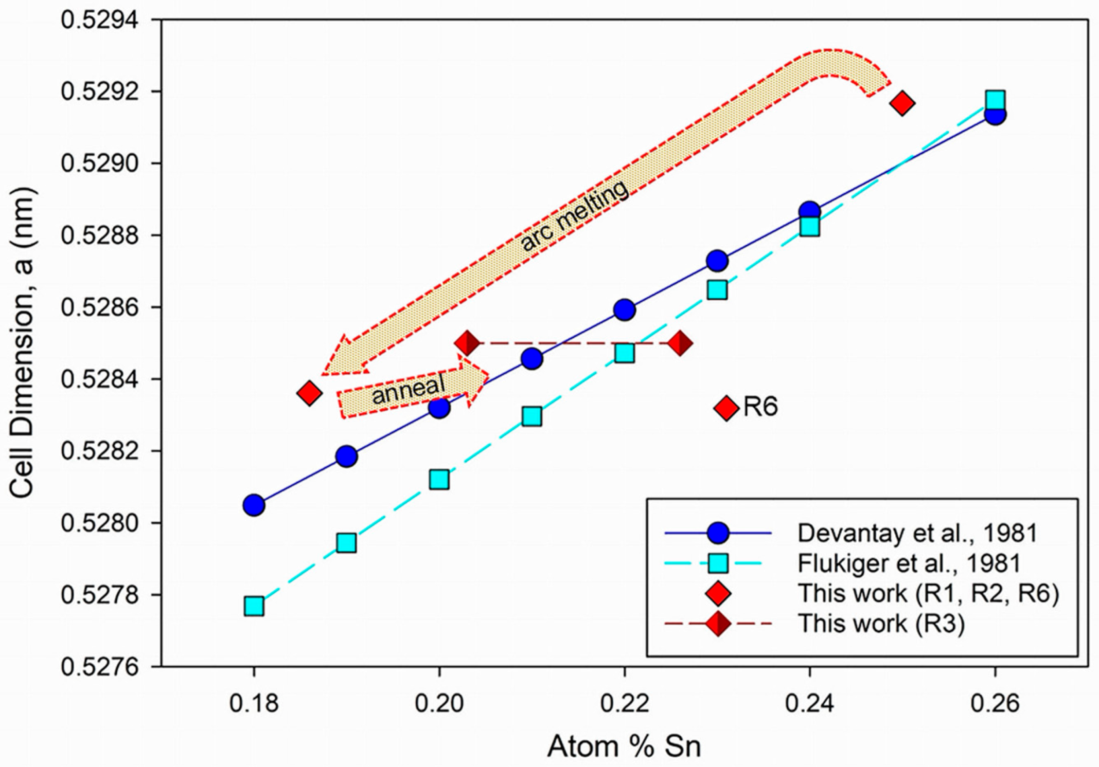
3.1. Crystallography and Phase Relations

Results from Rietveld refinement to quantitatively determine phase abundances are shown in Figure 1 for the XRD pattern from NS-1000/60/arc/ann/1000/60 (Run 3). The blue, red, and grey colours represent experimental, refined, and differences in models, respectively. As shown in Figure 1, Nb3Sn was the predominant phase (94.88%) with denoted indexed reflections, while a minor proportion of secondary phase such as niobium oxide was also observed (green symbols). Similar refinements were performed for all other samples, including those with a high proportion of Nb3Sn phase.
Table 2 shows the relative proportions of Nb3Sn and other products obtained from selected syntheses with a high proportion of Nb3Sn phase according to indexed XRD patterns. Refined XRD data including change in lattice parameters, weighted R factor (Rwp), and goodness of fit (gof) for each refinement are also shown in Table 2. Run 4 is not included in Table 2 because diffraction from a Nb3Sn phase was not observed. The sample from Run 5 was damaged during preparation for characterization and is also not included in Table 2.
In all cases, Nb3Sn was the major phase (in proportions above 85%) with minor amounts of other compounds including Nb and NbO. An increase in reaction time for NS-1000/60/arc/ann/1000/60 (Run 3) improves the yield of Nb3Sn due to complete conversion of excess Nb. The lattice parameter a decreased for arc-melted and annealed samples compared with a sample sintered at 1000 °C for 60 h (NS-1000/60; Run 1). Note the relatively high proportions of unreacted Nb for samples NS-1000/60/arc (Run 2) and NS-720/105/arc/ann/900/3 (Run 6).

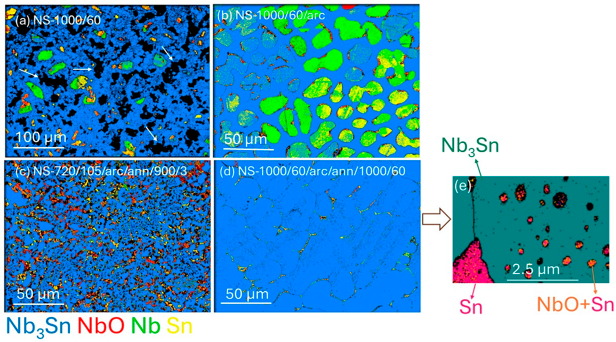
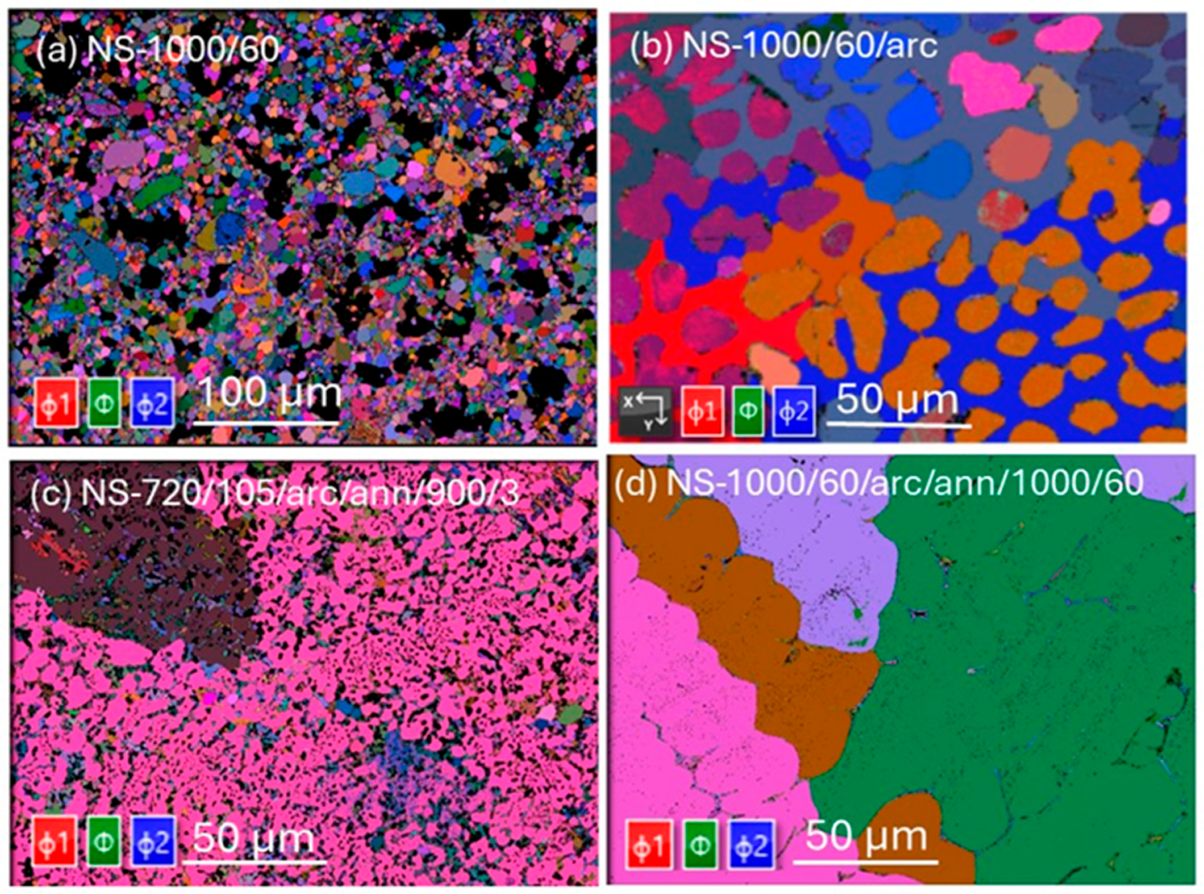
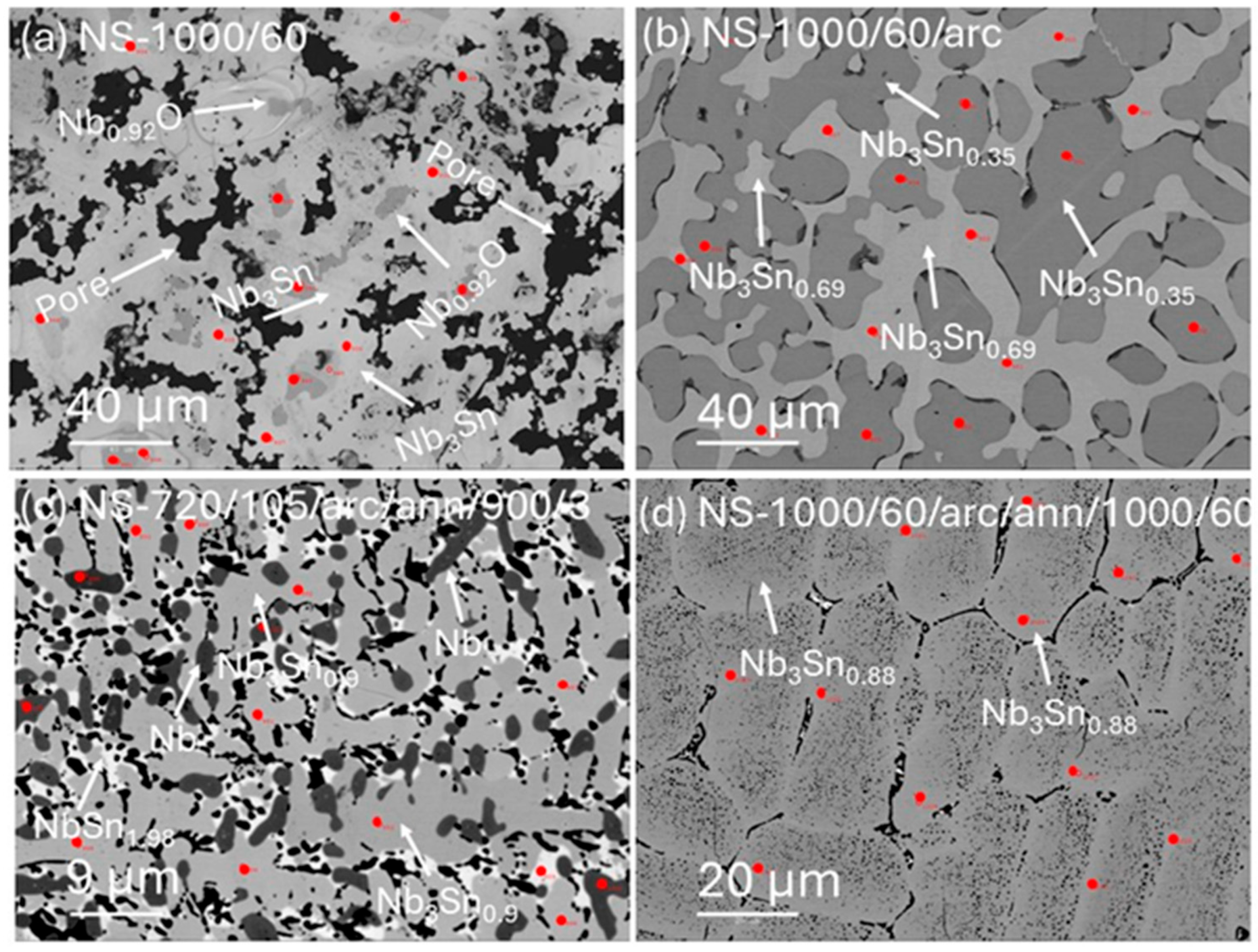
3.2. Microstructures and Grain Compositions

EBSD phase maps of Nb3Sn bulks for sintered, arc-melted, and annealed samples are shown in Figure 2. For all samples, Nb3Sn was the major phase and XRD Rietveld analyses confirmed that >85% of all samples were Nb3Sn. According to EBSD analysis, minor phases of Nb, Sn, and NbO were present in all samples. Diffraction peaks for Sn were not detected in the XRD patterns. The discrepancy in detecting Sn by diffraction methods may have been due to a localized presence on the surface of samples, low concentration, or an amorphous structure. In the latter case, Sn was detectable via EBSD but not by using XRD.
Irregular Nb3Sn crystals of <10 μm dimension were formed together with Nb and NbO in samples from NS-1000/60 (Figure 2a; Run 1). The presence of large Nb grains (>30 μm) indicated that an extended sintering process did not eliminate minor phases such as Nb or NbO. In Figure 2a, black areas (indicated by white arrows) indicate the presence of pores in these sintered samples. The microstructure of the NS-1000/60/arc (Figure 2b; Run 2) showed the formation of Nb and Sn phases along with Nb3Sn phase as well as a more consolidated microstructure with fewer pores than in Figure 2a. Most of the solidification morphologies due to arc-melting conditions possessed an approximately hemispherical shape.
Figure 2 indicates that arc melting provides higher-density products. Figure 2c clearly indicates that the Nb3Sn grains produced after annealing of the arc melted sample at 900 °C for 3 h (NS-720/105/arc/ann/900/3; Run 6) were significantly smaller (i.e., sub-micrometre to micrometre size) than those (i.e., >10 μm) produced at a higher temperature (1000 °C) and annealed for a longer time (60 h), as shown for NS-1000/60/arc/ann/1000/60 (Run 3). Extended annealing of the sample at the higher temperature of 1000 °C for 60 h resulted in densely packed and large grains (>50 μm) of Nb3Sn. This morphology was due to the significant grain growth, driven by increased atomic mobility at the higher annealing temperature over time.
Figure 3 shows Euler maps (determined by the EBSD technique) of Nb3Sn samples listed in Table 2. The Euler maps, which represent the crystallographic orientation of individual grains, reveal significant variations among the Nb3Sn bulk samples subjected to different heat treatments. For the sintered sample NS-1000/60 (Figure 3a), the map shows a wide range of orientations, indicating a lack of common crystallographic orientation among the grains. This Euler map suggests that the sintering process at 1000 °C for 60 h did not result in a uniform texture for all grains, including Nb3Sn.
The sample NS-720/105/arc/ann/900/3 (Run 6) displayed a more uniform crystallographic orientation with three predominant orientations observed for all grains in the field of view (Figure 3c). This texture indicated a more consistent grain orientation resulting from the annealing process. In contrast, the sample with extended annealing at 1000 °C for 60 h after arc-melting (NS-1000/60/arc/ann/1000/60) showed the presence of large Nb3Sn grains, each exhibiting distinct crystallographic orientations. This grain morphology confirms that prolonged annealing at high temperatures promotes grain growth, resulting in larger grains with diverse orientations. These observations highlight the significant impact of heat-treatment protocols on the crystallographic orientation and grain structure of Nb3Sn samples.
Figure 4 shows backscattered electron (BSE) images of four samples listed in Table 1. These BSE images display a broad range of image contrast typically attributed to fluctuations in the relative mean atomic number. Generally, regions appearing lighter in a BSE image have a higher atomic number than darker regions. This image contrast highlights microstructural changes in the Nb3Sn samples due to different processing and annealing conditions. For instance, the black colour delineates pores in the sample (Figure 4a), while the dark grey and brighter grey colours denote the Nb-rich and Sn-rich phases, respectively. In Figure 4a, the BSE image of NS-1000/60 (Run 2) reveals Nb3Sn aggregate surrounded by pores. These aggregates exhibit a distinctive pattern with a dark core and a lighter outer margin, corresponding to Nb-rich and Sn-rich phases, respectively.
A BSE image of the arc-melted sample (NS-1000/60/arc; Figure 4b) shows a darker Nb-rich area surrounded by lighter Sn-rich areas (arrowed). Figure 4c shows a BSE image of NS-720/105/arc/ann/900/3 (Run 6) with uniform structure and substantially smaller grain sizes compared with NS-1000/60 (Run 1) and NS-1000/60/arc (Run 2). The BSE image in Figure 4d shows that extended annealing of the arc-melted sample at 1000 °C for 60 h (NS-1000/60/arc/ann/1000/60; Run3) resulted in larger grains (i.e., >20 μm) compared to NS-720/105/arc/ann/900/3 (Figure 4c; Run 6). The BSE images in Figure 4 were used to guide locations for EPMA analyses, the locations of which are annotated by small red dots.
Table 3 provides average compositions from selected spot analyses for syntheses identified in Table 1. For each sample, the number of point analyses (n) used to obtain average compositions based on similar BSE image contrast is also listed in Table 3, along with corresponding average analytical totals that range from 98.7 to 99.8 (wt%) for the Nb–Sn phases. A majority of individual point analyses are Nb1−βSnβ phases, although other analyses are consistent with the presence of Nb and NbO in these samples.
In general, these data in Table 3 show that the concentration of Nb ranged from 34 to 100 at% and Sn from 10 to 66 at% across all analyses. As shown in Table 3, the stoichiometries of Nb–Sn phases included Nb3Sn, Nb3Sn0.90, Nb3Sn0.88, Nb3Sn0.69, Nb3Sn0.35 and NbSn1.98.

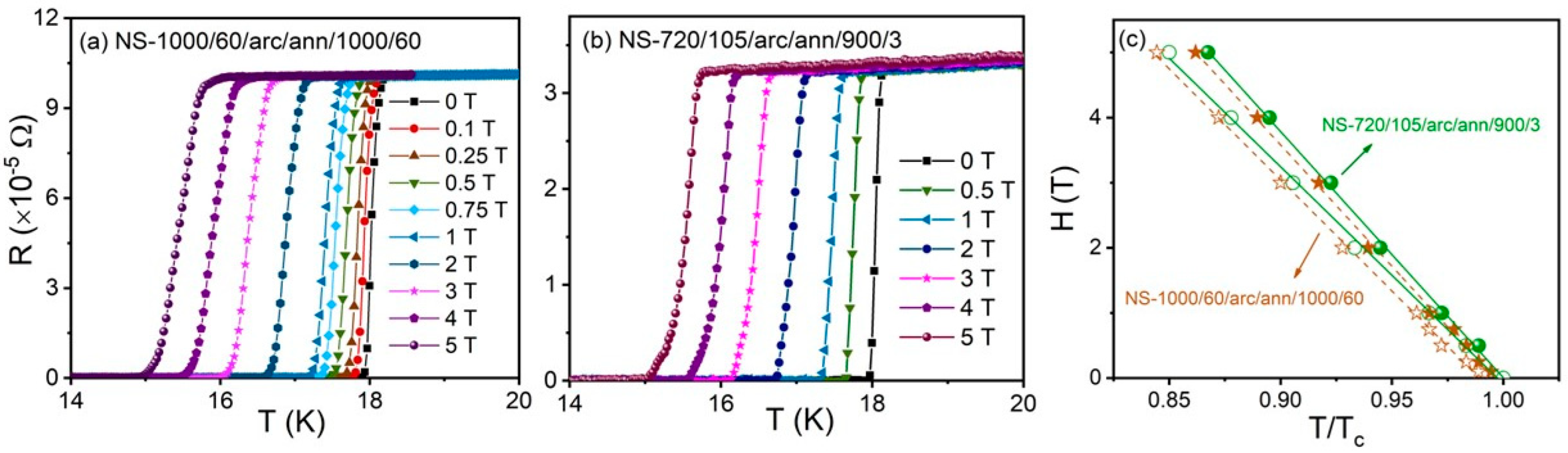
3.3. Electrical and Magnetic Properties

Figure 5a shows the zero-field-cooled and field-cooled measurements for Nb3Sn bulks under an applied magnetic field of 10 Oe. All samples showed a clear superconducting transition similar to that obtained previously [14]. NS-1000/60 (Run 1) and NS-720/105/arc/ann/900/3 (Run 6) demonstrated very sharp superconducting transitions at 16.45 K and 16.58 K, respectively. NS-1000/60/arc/ann/1000/60 (Run 3) showed a slightly lower transition temperature at 16.26 K. The arc-melted sample without further annealing (NS-1000/60/arc), showed a broad transition at 16.21 K followed by other transitions at 15.42 K and 6.78 K.
Figure 5b shows the field dependence of Jc for arc-melted samples (NS-1000/60/arc; Run 2) annealed at 900 °C for 3 h (NS-720/105/arc/ann/900/3; Run 6) and annealed at 1000 °C for 60 h (NS-1000/60/arc/ann/1000/60; Run 3). As shown in Figure 5b, the Jc of arc-melted Nb3Sn was much lower than the Jc of post-annealed Nb3Sn bulks. Both Nb3Sn bulk samples annealed at 900 °C and 1000 °C (NS-720/105/arc/ann/900/3 and NS-1000/60/arc/ann/1000/60) demonstrated enhanced Jc performance compared with only arc-melted Nb3Sn (NS-1000/60/arc).
Both annealed samples, NS-720/105/arc/ann/900/3 (Run 3) and NS-1000/60/arc/ann/1000/60 (Run 6), exhibited significantly enhanced critical current density (Jc), about 1.5 orders of magnitude greater compared with the arc-melted sample (NS-1000/60/arc; Run 2). NS-720/105/arc/ann/900/3 demonstrated the highest Jc across the entire field range up to 5 T, with Jc = 6.16 A/cm2 at 0.17 T and 10 K. Specifically, at 10 K, the low-field and high-field Jc values for NS-720/105/arc/ann/900/3 (Run 6) were 1.8 times and 5.8 times higher, respectively, than comparable values for NS-1000/60/arc/ann/1000/60 (Run 3).
The range of Jc values between 6.16 and 3.4 × 10⁴ A/cm2 for the two post-arc melt annealed samples (Run 6 and Run 3, respectively at low field) was comparable to values obtained in early experiments on Nb3Sn wires (e.g., produced by the bronze or PIT techniques) [7,23]. However, the Jc values reported in this present study for binary bulk Nb3Sn were an order of magnitude less than existing wires. There are limited available data on the Jc of bulk binary Nb3Sn obtained at 10 K.
Electrical resistance, R, versus temperature, T, curves for samples from NS-720/105/arc/ann/900/3 (Run 6) and NS-1000/60/arc/ann/1000/60 (Run 3) in the presence of magnetic fields up to 5 T are shown in Figure 6a,b. Electrical resistance started to drop toward zero at Tc= 18.0 K in zero magnetic field for both samples. This value aligns well with reports for the onset of superconductivity at 18.05 K ± 0.1 reported by Matthias et al. [1]. The onset of Tc decreased with the increasing magnetic field, while the transition width, ΔTc, increased from 0.1 K to 0.4 K for both samples, as shown in Figure 6a,b.
Figure 6c shows estimates for the upper critical field, Hc2, defined by R(T, Hc2) = 0.9Rn, representing the normal state resistance measured just above the onset of the critical temperature. Similarly, the irreversibility field, Hirr, is defined by R(T,Hirr) = 0.1Rn and is also shown in Figure 6c. From Figure 6c, we calculated slopes of 2.09 and 1.89 for dHc2/dT and dHirr/dT, respectively, for NS-720/105/arc/ann/900/3 (Run 6). Similarly, NS-1000/60/arc/ann/1000/60 (Run 3) yielded values of 2.05 and 1.85 T/K for dHc2/dT and dHirr/dT.
The Hc2 (0) was estimated using the Werthamer–Helfand–Hohenberg formula, Hc2 = −0.69Tc(dHc2/dT), with dHc2/dT at T = Tc. Using this formula, values for Hc2(0) = 26.1 and 25.6 T were obtained for the sample from NS-720/105/arc/ann/900/3 (Run 6) and NS-1000/60/arc/ann/1000/60 (Run 3), respectively. These values were lower than the reported value of 28.7 T for 23.6 ± 0.7 at.% Sn composition variation, noting that bulk samples in the study by Jewell et al. [24] were obtained using HIP techniques at 1020 °C on powder-in-tube samples, followed by post-HIP heat treatment at 1800 °C for 24 h.

4. Discussion

In this work, we describe combinations of sintering, arc-melting, and annealing procedures that affect the morphology, stoichiometry and superconducting properties of bulk Nb3Sn samples. Sintering of Sn and Nb is undertaken prior to arc melting in order to mitigate Sn evaporation at higher temperatures. The Nb–Sn phase diagram indicates that the superconducting Nb1−βSnβ phase occurs within the range for 0.18 < β < 0.25 for which 6 K < Tc < 18 K [5]. This phase can be synthesized either above 930 °C in the presence of a Sn–Nb melt or below this temperature through solid-state reactions involving Nb and Nb6Sn5 or NbSn2 [12].

4.1. Structure and Composition

The formation of Nb3Sn was not favourable for the sample sintered at 720 °C for 105 h because the diffusion of Nb and Sn was relatively slow. However, Nb3Sn was a primary phase of the sample sintered at 1000 °C (NS-1000/60) prior to arc melting, according to XRD and EBSD phase analysis. A higher sintering temperature of 1000 °C prior to arc melting promoted faster diffusion and effective transformation of the starting mixture. After arc melting, the sample showed a high proportion of Nb3Sn phase and the presence of residual Nb and Sn (as shown in Figure 2b, Figure 3b and Figure 4b), albeit with a lower proportion of Nb3Sn compared with Run 1 or Run 3. In addition, EPMA analyses (Table 3) show that individual grains are marginally within the superconducting range for Nb1−βSnβ phases (i.e., β =18.6 (1)).
Post-annealing serves as an important step to stabilize metastable phases that form during quenching and facilitates the formation of the target composition. In both cases, for Run 3 and Run 6, annealing after arc melting resulted in compositions of Nb1−βSnβ phases within the superconducting range [5]. However, a substantial difference in grain size was observed between the samples. Annealing of NS-720/105/arc/ann/900/3 (Run 6) at 900 °C yielded a uniform microstructure with smaller (<5 μm) grain sizes.
A uniform microstructure (i.e., similar grain orientation) influences macroscopic mechanical properties such as elasticity and strain distribution as well as critical current [25]. This influence competes with an increased density of grain boundaries in bulk polycrystalline samples of Nb3Sn, such as from Run 6. Smaller grain size, to the sub-micrometer scale, also results in substantial improvement to Jc values in wires produced in ternary systems such as Nb1−βSnβX (where X = Cu, Ti, Ta, Zr) [23,26,27]. We suggest that the same principles apply to production of bulk binary Nb3Sn.
Goedeke [5] provided a comprehensive and informative review of early experiments on production of homogenous Nb3Sn, noting that the general variation of superconducting properties for A15 compounds consistently depended on cell dimension, atomic content (for Nb1-βSnβ, the value of β), normal state resistivity, and long-range order. Figure 7 is an adaptation of Figure 3 in [5], showing the variation of lattice parameter, a, with atomic content of Sn in Nb1−βSnβ. Figure 7 includes average data for individual grains within the four samples that showed compositions within the range 0.18 < β < 0.25 (Table 3).
Figure 7 suggests that pre-treatment of Nb–Sn ingots before arc melting combined with post-treatment annealing may enable production of bulk Nb1−βSnβ with a targeted stoichiometry. For example, Rietveld (Table 2) and EPMA compositional (Table 3) analyses show that Run 1 produced a predominantly β = 0.25 compound with pre-treatment. Arc melting of this sample produced a mixture with lower proportions of Nb1−βSnβ with β = 0.186 and substantial Nb. Annealing after arc melting resulted in a sample with high proportions of two Nb1−βSnβ compounds (Table 3) with β = 0.226 and β = 0.203. These trends are shown in Figure 7 by the broad dotted red arrows and suggest that further attention to annealing times post-arc melting could result in a bulk single-phase Nb1−βSnβ compound.
The optimum annealing times and appropriate temperatures to maximize single-phase Nb3Sn remains uncertain based on data obtained to date. Nevertheless, the example of Run 6, from which predominantly Nb1−βSnβ formed with β = 0.231 after a lower pre-treatment temperature and very short annealing time, implies that within the extremes of processing represented by Run 3 and Run 6, evaluation of these parameters indicates potential for scalable production of bulk Nb3Sn. In the latter case, smaller micrometer-scale grain size and enhanced Jc compared with other samples in this study suggest that annealing times of 3 h < tpost < 60 h at temperatures between 900 °C and 1000 °C are viable targets for future experiments. Future processing and microstructural studies would benefit from experimental determination of macroscopic properties [25] and electronic property calculations informed by defect identifications [28], as well as in situ XPS techniques [29], scanning Hall probe microscopy [30] and a range of Synchrotron experiments [31,32,33].

4.2. Superconductivity

The arc-melted sample for NS-1000/60/arc (Run 2) exhibited a wide superconducting transition at 16.21 K, accompanied by additional transitions at 15.42 K and 6.78 K. The low Tc = 6.78 K could have been due to formation of a solid solution with lower Tc associated with lower Sn content (β = 0.104) as indicated by EPMA data (see Table 3). It has been reported that at low concentrations (β < 0.05 for Nb1-βSnβ), the incorporation of Sn into Nb forms a solid solution that lowers the Tc of Nb from 9.2 K to approximately 4 K for β = 0.05 [5,12,34].
In the A15 Nb3Sn structure, which had a lattice parameter of about 0.529 nm for the stoichiometric composition [8], the separation between Nb atoms was roughly 0.265 nm. Reduced distance between Nb atoms in the chains is believed to create a confined peak in the d-band density of states (DOS), resulting in a notably increased DOS near the Fermi level. This enhancement is thought to play a role in the higher critical temperature (Tc) of Nb3Sn compared to other Nb-based superconductors. Additionally, it has been observed that excess Nb atoms can occupy Sn sites, leading to anti-site disorder [35].
Ab initio density functional theory (DFT) calculations by Besson et al. [22] reveal that Nb3Sn essentially appears as an anti-site compound, with the density of vacancies, particularly Sn vacancies, remaining negligible below the melting temperature [36]. Additionally, an EXAFS study examining the occupancy of Ta/Ti sites in Nb3Sn wires revealed that the top-performing Ti-doped strand was considerably sub-stoichiometric in Sn [37]. This anti-site disorder is likely to be responsible for the high average behaviour of the upper critical field (Hc2). EPMA analyses (Table 3) showed non-stoichiometric compositions in samples from Runs 2, 3, and 6; implicit confirmation that the density of vacancies and/or anti-site disorder influence electronic properties of Nb1−βSnβ compounds, as noted previously [5]. These findings as well as detailed computational studies [38] suggest that dopants and anti-site disorder play a crucial role in minimizing the variability of superconducting properties and maximizing high-field Jc properties.
Table 4 shows a comparison between experimental data and calculated Tc using DFT from the work of Carlson et al. [39] and Tc values obtained for samples in this work. The Sn concentration according to EPMA results (Table 3) can be correlated with the experimental determination of Tc [20]. For both the DFT calculations and the experimental results in our work, Tc values increased with increasing Sn concentration. The calculated Tc and the Fermi-level DOS showed strong agreement across all Sn concentrations [39]. The presence of Sn anti-site defects is believed to significantly broaden a reduction in the density of states (DOS) at the Fermi level near grain boundaries [39]. This presence of anti-site defects may explain the reduction in Tc from 16.58 K for Nb3.00Sn (NS-1000/60; Run 1) to 16.25 K for Nb3Sn0.88 + Nb3Sn0.77 (NS-1000/60/arc/ann/1000/60; Run 3).
The Jc of a bulk superconductor in a magnetic field is governed by the pinning force (Fp) generated by appropriately sized crystal defects that hinder the movement of magnetic vortices. The efficiency of pinning is highest when defects approach the coherence length of the superconductor, typically 2–4 nm for Nb3Sn [40]. Defects smaller or larger than this size result in reduced pinning efficiency. Grain boundaries, which are the regions where different crystal grains meet, can also act as pinning centres for magnetic flux lines. The significant impact of grain boundaries on the superconducting properties of Nb3Sn is widely recognized [41,42]. These boundaries play a crucial role in pinning vortices and determining critical currents in Nb3Sn wires, as documented in previous studies [5,43,44] and experimentally demonstrated using atom probe tomography combined with Jc measurements on Nb3Sn wires synthesized by the internal tin process [41].
The enhanced Jc of the bulk sample from NS-720/105/arc/ann/900/3 (Run 6) related to the formation of smaller grains (i.e., <5 μm) and the higher density of grain boundaries compared with the arc melted and post-annealed Nb1−βSnβ sample synthesized at higher temperature. The NS-1000/60 (Run 1) and NS-1000/60/arc (Run 2) with large grains showed a lower Jc compared with NS-720/105/arc/ann/900/3 (Run 6), especially at higher magnetic fields.
Simulation by Carlson et al. [39] demonstrated that grain boundaries serve a dual role, acting as nucleation points for vortex entry and as pinning sites once vortices have formed. The behaviour of the vortices depends on the strength of the applied field—vortices can either stay pinned at the grain boundaries or pass into the grains. This interpretation is consistent with higher supercurrent loss for NS-1000/60/arc/ann/1000/60 (Run 3) compared with NS-720/105/arc/ann/900/3 (Run 6) for H > 2 T. Additionally, observations have revealed compositional variations within Nb3Sn grain boundaries at a nanometer scale [45,46] that affect the supercurrent performance of Nb3Sn superconducting wires. Among the samples studied, NS-720/105/arc/ann/900/3 (Run 6) with an average Nb3Sn0.9 composition showed the highest supercurrent performance. This performance, as noted above, was due to the high density of grain boundaries (Figure 3c and Figure 4c) and may have been additionally enhanced by the presence of anti-site defects.

5. Conclusions

This investigation explored the impact of synthesis procedures using pre-treatment, arc melting, and post-arc-melt annealing on the morphology, grain boundary formation, and stoichiometry of binary Nb1−βSnβ bulk superconductors. Arc-melted the sample annealed at 900 °C for 3 h (β = 0.231) resulted in enhancement of Tc and Jc compared with other samples in this work. This enhancement was attributed to recrystallization of smaller grains and formation of effective pinning centres such as a higher proportion of grain boundaries and anti-site defects. However, annealing at 1000 °C for 60 h after arc melting reduced Jc. A decrease in Tc from 16.58 K for Nb3.00Sn in a sintered binary sample to 16.25 K for an arc-melted and annealed sample was attributed to the production of two Nb1−βSnβ compounds (β = 0.226 and β = 0.203) with a large grain size (>50 μm) and no Nb. The success of these two alternate synthesis procedures involving pre-treatment sintering, followed by arc melting and subsequent annealing at high temperature (>900 °C) for different times suggest that further exploration of sintering and annealing conditions offers potential for scalable production of bulk Nb1−βSnβ compounds of predictable stoichiometry.

Author Contributions

M.S.: conceptualization, formal analysis, methodology, investigation, supervision, funding acquisition, writing—original, review and editing; H.E.C.: EPMA methodology and analysis, investigation, validation, and visualization; A.D.M.: methodology, investigation, resources, validation; J.A.: investigation, formal analysis, review and editing; I.D.R.M.: conceptualization, formal analysis, funding acquisition, validation, visualization, writing—review and editing. All authors have read and agreed to the published version of the manuscript.

Funding

This research was partially funded by an Advance Queensland Research Fellowship from the Queensland Government to M.S. and from the Australian Government agency ARENA as part of Contract No. 2018/RND012. The views expressed herein are not necessarily the views of the Australian Government, and the Australian Government does not accept responsibility for any information or advice contained herein.

Institutional Review Board Statement

Not applicable.

Informed Consent Statement

Not applicable.

Data Availability Statement

The original contributions presented in this study are included in the article. Further inquiries can be directed to the corresponding author. Comprehensive EPMA results can be provided upon request.

Acknowledgments

The authors are grateful to the Central Analytical Research Facility at Queensland University of Technology for access to characterization facilities. During the preparation of this manuscript and study, the author(s) did not use any artificial intelligence tools. The authors have reviewed and edited the output and take full responsibility for the content of this publication.

Conflicts of Interest

The authors declare no conflicts of interest.

References

  1. Matthias, B.T.; Geballe, T.H.; Geller, S.; Corenzwit, E. Superconductivity of Nb3Sn. Phys. Rev. 1954, 95, 1435. [Google Scholar] [CrossRef]
  2. Miyazaki, T.; Matsukura, N.; Miyatake, T.; Shimada, M.; Takabatake, K.; Itoh, K.; Kiyoshi, T.; Sato, A.; Inoue, K.; Wada, H. Development of Bronze-Processed Nb3Sn Superconductors for 1 GHz NMR Magnets. In Advances in Cryogenic Engineering Materials; Balachandran, U.B., Gubser, D.G., Hartwig, K.T., Reed, R.P., Warnes, W.H., Bardos, V.A., Eds.; Springer: Boston, MA, USA, 1998; pp. 935–941. [Google Scholar]
  3. Tommasini, D. Nb3Sn Accelerator Dipole Magnet Needs for a Future Circular Collider. In Nb3Sn Accelerator Magnets: Designs, Technologies and Performance; Schoerling, D., Zlobin, A.V., Eds.; Springer International Publishing: Cham, Switzerland, 2019; pp. 427–439. [Google Scholar]
  4. Mitchell, N.; Breschi, M.; Tronza, V. The use of Nb3Sn in fusion: Lessons learned from the ITER production including options for management of performance degradation. Supercond. Sci. Technol. 2020, 33, 054007. [Google Scholar] [CrossRef]
  5. Godeke, A. A review of the properties of Nb3Sn and their variation with A15 composition, morphology and strain state. Supercond. Sci. Technol. 2006, 19, R68–R80. [Google Scholar] [CrossRef]
  6. Sun, W.; Cheng, J.; Chen, S. Preparation and Superconducting Properties of Nb3Sn by Mechanical Alloying. J. Low Temp. Phys. 2021, 205, 100–111. [Google Scholar] [CrossRef]
  7. Flükiger, R.; Uglietti, D.; Senatore, C.; Buta, F. Microstructure, composition and critical current density of superconducting Nb3Sn wires. Cryogenics 2008, 48, 293–307. [Google Scholar] [CrossRef]
  8. Devantay, H.; Jorda, J.L.; Decroux, M.; Muller, J.; Flükiger, R. The physical and structural properties of superconducting A15-type Nb-Sn alloys. J. Mater. Sci. 1981, 16, 2145–2153. [Google Scholar] [CrossRef]
  9. Flükiger, R.; Schauer, W.; Specking, W.; Schmidt, B.; Springer, E. Low-Temperature Phase-Transformation in Nb3Sn Multifilamentary Wires and the Strain Dependence of their Critical Current-Density. IEEE Trans. Magn. 1981, 17, 2285–2288. [Google Scholar] [CrossRef]
  10. Cheng, J.; Wang, Q.; Wang, H.; Dai, Y. Microstructure evolution of Nb3Sn superconductors during diffusion treatment by bronze route. Rare Met. 2012, 31, 446–450. [Google Scholar] [CrossRef]
  11. Wu, B.; Guo, Q.; Wang, C.G.; Chen, J.Y.; Li, Z.; Shi, Y.G.; Liu, X.H.; Feng, Y.; Yan, G.; Li, J.F.; et al. Investigation on the Recrystallization and Nb3Sn Microstructure of Nb Alloys with Large Deformation During Heat Treatment. IEEE Trans. Appl. Supercond. 2024, 34, 5. [Google Scholar] [CrossRef]
  12. Banno, N. Low-temperature superconductors: Nb3Sn, Nb3Al, and NbTi. Superconductivity 2023, 6, 100047. [Google Scholar] [CrossRef]
  13. Goldacker, W.; Ahrens, R.; Nindel, M.; Obst, B.; Meingast, C. HIP Sythesized Nb3Sn Bulk Materials with Extraordinary Homogeneity. IEEE Trans. Appl. Supercond. 1993, 3, 1322–1325. [Google Scholar] [CrossRef]
  14. Zhou, J.; Jo, Y.; Hawn Sung, Z.; Zhou, H.; Lee, P.J.; Larbalestier, D.C. Evidence that the upper critical field of Nb3Sn is independent of whether it is cubic or tetragonal. Appl. Phys. Lett. 2011, 99, 122507. [Google Scholar] [CrossRef]
  15. Jain, D.; Sudarsan, V.; Tyagi, A.K. Synthesis of Metallic Materials by Arc Melting Technique. In Handbook on Synthesis Strategies for Advanced Materials: Volume-I: Techniques and Fundamentals; Tyagi, A.K., Ningthoujam, R.S., Eds.; Springer: Singapore, 2021; pp. 197–213. [Google Scholar]
  16. Kirschen, M.; Hay, T.; Echterhof, T. Process Improvements for Direct Reduced Iron Melting in the Electric Arc Furnace with Emphasis on Slag Operation. Processes 2021, 9, 402. [Google Scholar] [CrossRef]
  17. Singh, R. (Ed.) Chapter 5—Production of Steel. In Applied Welding Engineering, 2nd ed.; Butterworth-Heinemann: Waltham, MA, USA, 2016; pp. 37–55. [Google Scholar]
  18. Konushkin, S.V.; Kolmakov, A.G.; Nasakina, E.O.; Sergienko, K.V.; Sevost’yanov, M.A. Production of a Ti-20 at % Nb-5 at % Ta Alloy in an Argon Arc Furnace. Russ. Metall. 2022, 2022, 569–574. [Google Scholar] [CrossRef]
  19. Feng, J.; Wang, X.; Song, K.X. Improving the mechanical properties of WC/Cu composites through vacuum consumable arc melting. Mater. Lett. 2025, 384, 137966. [Google Scholar] [CrossRef]
  20. Gonçalves, V.R.M.; Lisboa, P.N.; Afonso, C.R.M. Unravelling microstructure of novel as-cast in-situ a Ti and β Ti-Nb alloy matrix composites with NbC addition. Mater. Lett. 2023, 349, 134794. [Google Scholar] [CrossRef]
  21. Drouin, D.; Couture, A.R.; Joly, D.; Tastet, X.; Aimez, V.; Gauvin, R. CASINO—V2.42—A Fast and Easy to Use Modeling Tool for Scanning Electron Microscopy and Microanalysis Users. Scanning 2007, 29, 92–101. [Google Scholar] [CrossRef]
  22. Polichetti, M.; Galluzzi, A.; Kumar, R.; Goyal, A. Equation for Calculation of Critical Current Density Using the Bean’s Model with Self-Consistent Magnetic Units to Prevent Unit Conversion Errors. Materials 2025, 18, 269. [Google Scholar] [CrossRef]
  23. Xu, X.C. A review and prospects for Nb3Sn superconductor development. Supercond. Sci. Technol. 2017, 30, 093001. [Google Scholar] [CrossRef]
  24. Jewell, M.C.; Godeke, A.; Lee, P.J.; Larbalestier, D.C. The upper critical field of stoichiometric and off-stoichiometric bulk, binary Nb3Sn. In Proceedings of the Joint Cryogenic Engineering Conference/International Cryogenic Materials Conference (CEC-ICMC), Anchorage, AK, USA, 22–26 September 2003; pp. 474–481. [Google Scholar]
  25. Ding, H.; Gao, Y. Analysis of the strain dependence of the superconducting critical properties of single-crystal and polycrystalline Nb3Sn. Supercond. Sci. Technol. 2021, 34, 075006. [Google Scholar] [CrossRef]
  26. Sumption, M.D.; Bhartiya, S.; Kovacks, C.; Peng, X.; Gregory, E.; Tomsic, M.J.; Collings, E.W. Critical current density and stability of Tube Type Nb3Sn conductors. Cryogenics 2012, 52, 91–99. [Google Scholar] [CrossRef]
  27. Xu, X.C.; Sumption, M.D.; Peng, X. Internally Oxidized Nb3Sn Strands with Fine Grain Size and High Critical Current Density. Adv. Mater. 2015, 27, 1346–1350. [Google Scholar] [CrossRef] [PubMed]
  28. Wu, L.N.; Yang, S.T.; Shen, J.K.; Zhang, J.S.; Liu, F.H. Coexistence of superconductivity and charge density wave instability in A15-Nb3Sn. Phys. Chem. Chem. Phys. 2023, 25, 32452–32459. [Google Scholar] [CrossRef] [PubMed]
  29. Cano, A.; Eremeev, G.V.; Zuazo, J.R.; Lee, J.Y.; Luo, B.; Martinello, M.; Romanenko, A.; Posen, S. Selective Thermal Evolution of a Native Oxide Layer in Nb and Nb3Sn-Coated SRF Grade Nb: An In Situ XPS Study. J. Phys. Chem. C 2023, 127, 19705–19716. [Google Scholar] [CrossRef]
  30. Pfeiffer, S.; Baumgartner, T.; Löffler, S.; Stöger-Pollach, M.; Hopkins, S.C.; Ballarino, A.; Eisterer, M.; Bernardi, J. Analysis of inhomogeneities in Nb3Sn wires by combined SEM and SHPM and their impact on Jc and Tc. Supercond. Sci. Technol. 2023, 36, 045008. [Google Scholar] [CrossRef]
  31. Arul, K.T.; Chang, H.W.; Shiu, H.W.; Dong, C.L.; Pong, W.F. A review of energy materials studied by in situ/operando synchrotron x-ray spectro-microscopy. J. Phys. D Appl. Phys. 2021, 54, 343001. [Google Scholar] [CrossRef]
  32. Magdy, M. A Brief Account of the Technology Significance of Synchrotron Radiation: A State-of-the-art Angle-Resolved Photoemission Spectroscopy (ARPES). Curr. Anal. Chem. 2025, 21, 1–9. [Google Scholar] [CrossRef]
  33. Qin, L.; Du, W.J.; Cipiccia, S.; Bodey, A.J.; Rau, C.; Mi, J.W. Synchrotron X-ray operando study and multiphysics modelling of the solidification dynamics of intermetallic phases under electromagnetic pulses. Acta Mater. 2024, 265, 119593. [Google Scholar] [CrossRef]
  34. Foner, S.; Schwartz, B. Superconductor Materials Science: Metallurgy, Fabrication, and Applications; Springer: New York, NY, USA, 1981. [Google Scholar]
  35. Welch, D.O.; Dienes, G.J.; Lazareth, O.W.; Hatcher, R.D. Defects and diffusion mechanisms in Nb3Sn. J. Phys. Chem. Solids 1984, 45, 1225–1242. [Google Scholar] [CrossRef]
  36. Besson, R.; Guyot, S.; Legris, A. Atomic-scale study of diffusion in A15 Nb3Sn. Phys. Rev. B 2007, 75, 054105. [Google Scholar] [CrossRef]
  37. Heald, S.M.; Tarantini, C.; Lee, P.J.; Brown, M.D.; Sung, Z.; Ghosh, A.K.; Larbalestier, D.C. Evidence from EXAFS for Different Ta/Ti Site Occupancy in High Critical Current Density Nb3Sn Superconductor Wires. Sci. Rep. 2018, 8, 4798. [Google Scholar] [CrossRef] [PubMed]
  38. Sitaraman, N.S.; Kelley, M.M.; Porter, R.D.; Liepe, M.U.; Arias, T.A.; Carlson, J.; Pack, A.R.; Transtrum, M.K.; Sundararaman, R. Effect of the density of states at the Fermi level on defect free energies and superconductivity: A case study of Nb3Sn. Phys. Rev. B 2021, 103, 115106. [Google Scholar] [CrossRef]
  39. Carlson, J.; Pack, A.; Transtrum, M.K.; Lee, J.; Seidman, D.N.; Liarte, D.B.; Sitaraman, N.S.; Senanian, A.; Kelley, M.M.; Sethna, J.P. Analysis of magnetic vortex dissipation in Sn-segregated boundaries in Nb3Sn superconducting RF cavities. Phys. Rev. B 2021, 103, 024516. [Google Scholar] [CrossRef]
  40. Xu, X.; Peng, X.; Rochester, J.; Lee, J.-Y.; Sumption, M. High critical current density in internally-oxidized Nb3Sn superconductors and its origin. Scr. Mater. 2020, 186, 317–320. [Google Scholar] [CrossRef]
  41. Banno, N.; Morita, T.; Yu, Z.; Yagai, T.; Tachikawa, K. Effect of Zn addition and Ti doping position on the diffusion reaction of internal tin Nb3Sn conductors. Supercond. Sci. Technol. 2019, 32, 115017. [Google Scholar] [CrossRef]
  42. Qu, P.S.; Li, S.L.; Liu, G.B.; Sun, X.G.; Xu, M.; Liu, L.; Chen, Y.L.; Wang, W.T.; Zhang, Y.; Feng, Y.; et al. Critical current density enhancement of Nb3Sn superconducting wires by incorporating oxygen through rapid-heating method. Mater. Lett. 2023, 341, 134157. [Google Scholar] [CrossRef]
  43. Scanlan, R.M.; Fietz, W.A.; Koch, E.F. Flux pinning centers in superconducting Nb3Sn. J. Appl. Phys. 2008, 46, 2244–2249. [Google Scholar] [CrossRef]
  44. Talantsev, E.F.; Valova-Zaharevskaya, E.G.; Deryagina, I.L.; Popova, E.N. Characteristic Length for Pinning Force Density in Nb3Sn. Materials 2023, 16, 5185. [Google Scholar] [CrossRef]
  45. Suenaga, M.; Jansen, W. Chemical compositions at and near the grain boundaries in bronze-processed superconducting Nb3Sn. Appl. Phys. Lett. 1983, 43, 791–793. [Google Scholar] [CrossRef]
  46. Sandim, M.J.R.; Tytko, D.; Kostka, A.; Choi, P.; Awaji, S.; Watanabe, K.; Raabe, D. Grain boundary segregation in a bronze-route Nb3Sn superconducting wire studied by atom probe tomography. Supercond. Sci. Technol. 2013, 26, 055008. [Google Scholar] [CrossRef]
Figure 1. Rietveld refinement of the XRD pattern for NS-1000/60/arc/ann/1000/60 (Run 3). The blue, red, and grey colours represent experimental, refined, and differences in models, respectively. Reflections for Nb3Sn are indexed. The green symbols indicate peaks for NbO.
Materials 18 03050 g001
Figure 2. EBSD phase maps of Nb1−βSnβ aggregates showing (a) NS-1000/60 (Run 1), (b) NS-1000/60/arc (Run 2), (c) NS-720/105/arc/ann/900/3 (Run 6), (d) NS-1000/60/arc/ann/1000/60 (Run 3), (e) higher-magnification EBSD phase map of small black areas for NS-1000/60/arc/ann/1000/60. The white arrows in (a) denote holes in NS-1000/60. Colour scheme for (ad) matches the compound legend below (c): Nb3Sn—blue; NbO—red; Nb—green; Sn—yellow. (e) Nb3Sn—green; Sn—red; NbO + Sn—orange plus red.
Materials 18 03050 g002
Figure 3. Euler maps of (a) NS-1000/60 (Run 1), (b) NS-1000/60/arc, (Run 2), (c) NS-720/105/arc/ann/900/3 (Run 6), (d) NS-1000/60/arc/ann/1000/60 (Run 3). Euler angles are characterized by rotation of φ1 about the z-axis (red), rotation of φ about the rotated x-axis (green), and rotation φ2 about the y-axis (blue). The same color signifies similar grain orientation; non-primary colors indicate intermediate orientations.
Materials 18 03050 g003
Figure 4. Backscattered electron images of (a) NS-1000/60 (Run 1), (b) NS-1000/60/arc (Run2), (c) NS-720/105/arc/ann/900/3 (Run 6) and (d) NS-1000/60/arc/ann/1000/60 (Run 3). The white arrows denote holes, Nb-rich, and Sn-rich areas. Red circles indicate locations of spot analyses using EPMA. Note the difference in scale bars within Figure 4.
Materials 18 03050 g004
Figure 5. (a) ZFC magnetization of Nb3Sn from NS-1000 (blue), NS-1000/60/arc (orange), NS-720/105/arc/ann/900/3 (maroon), NS-1000/60/arc/ann/1000/60 (green) and (b) critical current density of the same Nb3Sn samples as a function of an applied magnetic field at 10 K.
Materials 18 03050 g005
Figure 6. Temperature dependence of resistance for (a) NS-720/105/arc/ann/900/3 (Run 6) and (b) NS-1000/60/arc/ann/1000/60 (Run 3) under different magnetic fields up to 5 T. (c) Hc2 (closed symbol) and Hirr (open symbol) versus temperature for NS-720/105/arc/ann/900/3 (green) and NS-1000/60/arc/ann/1000/60 (orange).
Materials 18 03050 g006
Figure 7. Refined cell dimensions plotted against Sn content for Nb1−βSnβ samples listed in Table 3 (red diamonds). Linear plots for Nb1−βSnβ obtained in other studies ([8] blue solid line; [9] cyan dotted line); The trajectory by [8] is preferred by Goedeke [5]. Estimated standard errors for data from this study are within the symbol size. Note the statistically equivalent number of compositions for samples from Run 3, which straddle the trajectories determined by Devantnay et al. [8] and Flükiger et al. [9]. Adapted from Figure 3 of Goedeke [5] with permission.
Materials 18 03050 g007
Table 1. Sample ID, synthesis technique and heat treatment conditions for Nb3Sn samples.
RunSample IDSintering
Condition
Arc-MeltPost Arc-Melt
Heat Treatment
1NS-1000/601000 °C/60 hNoNo
2NS-1000/60/arc1000 °C/60 hYesNo
3NS-1000/60/arc/ann/1000/601000 °C/60 hYes1000 °C/60h
4NS-720/105720 °C/105 hNoNo
5NS-720/105/arc720 °C/105 hYesNo
6NS-720/105/arc/ann/900/3720 °C/105 hYes900 °C/3h
Table 2. Relative phase proportions and lattice parameters determined by Rietveld refinements.
RunSample IDNb3Sn (%)NbO (%)Nb (%)Unit Cell * (Å)Rwp (%)gof
1NS-1000/6094.693.571.745.29167(3)13.81.5
2NS-1000/60/arc85.164.8010.045.28360(5)13.51.6
3NS-1000/60/arc/ann/1000/6094.885.12-5.28510(4)12.21.5
6NS-720/105/arc/ann/900/385.993.4910.525.28318(6)12.51.2
* Estimated standard deviation in parentheses to the least significant figure.
Table 3. Average compositions of selected grains in Nb–Sn samples determined by EPMA.
Samplen **Element Atom %Totals (wt%)Stoichiometry
NbSnOTotal NbSnO
NS-1000/60 (R1)
Nb3Sn1.002175.0 (2)25.0 (2)-10098.7 (4)31.00 (1)-
Nb0.92O947.9 (7)-52.1 (7) *1001000.92-1
Nb5100.0--100 1--
NS-1000/60/arc (R2)
Nb3Sn0.692081.4 (1)18.6 (1)-10099.6 (3)30.69 (1)-
Nb3Sn0.352089.6 (2)10.4 (2)-10099.5 (2)30.35 (1)-
NS-1000/60/arc/ann/1000/60 (R3)
Nb3Sn0.88977.4 (6)22.6 (6)-10099.8 (2)30.88 (3)-
Nb3Sn0.771079.7 (4)20.3 (4)-10099.7 (3)30.77 (2)-
NS-720/105/arc/ann/900/3 (R6)
Nb3Sn0.902176.9 (3)23.1 (3)-10099.8 (2)30.90 (2)-
Nb1Sn1.98533.6 (4)66.4 (4)-10098.7 (4)11.98 (3)-
* Oxygen calculated by difference from 100; ** n is the number of point analyses used to obtain average composition; values in parentheses are one standard deviation to the least significant figure. Weight percentage totals provide an indication of analytical precision.
Table 4. Calculated Tc versus measured Tc for different concentrations of Sn in Nb1-βSnβ.
Sn (at %) (Calc) [39]Tc (K) (Calc) [39]Tc (K) (Experiment) [39]Sn (at %)
(This Work)
Tc (K)
(This Work)
18.759.2618.606.78 *
20.8311.39.522.5916.26 *
23.4416.11623.0916.45 *
25.0018.21825.0216.58 *
* Tc obtained from ZFC and FC measurements.
Disclaimer/Publisher’s Note: The statements, opinions and data contained in all publications are solely those of the individual author(s) and contributor(s) and not of MDPI and/or the editor(s). MDPI and/or the editor(s) disclaim responsibility for any injury to people or property resulting from any ideas, methods, instructions or products referred to in the content.

