1. Introduction
Metal oxide films with controllable conduction and broadband transparency are quite appropriate for using with optical and electrical coatings. Among those coatings, titanium oxide (TiO
x) possesses a high refractive index with wide energy bandgap, making it an ideal candidate to be applied in the laminated optical structure, both at visible wavelengths and, in electronics, as a transparent dielectric layer [
1,
2,
3]. Moreover, TiO
x has low toxicity and bio-inertness as well as strong redox ability when illuminated by ultraviolet (UV) radiation, leading it to become a valuable surface modification layer in the environmental purification and biomedical engineering applications [
4,
5,
6,
7]. Redox complexes with strong oxidative and reduction potential, such as hydroxyl radical (·OH), superoxide radical (·O
2−), and hydrogen peroxide (H
2O
2), form on the UV-light-activated TiO
x surface as a consequence of the photo-generated electron–hole pairs (EHPs), reacting with the environmental vapor and oxygen to provide excellent photocatalysis for mineralizing pollutants and inhibiting bacterial growth. Thus far, researchers have sought to achieve a TiO
x film that possesses the anatase crystalline structure with a maximized specific surface area through adequate deposition and/or post-annealing processes that behave as a nanotextured surface [
8,
9,
10]. In addition to engineering the TiO
x film’s crystallinity and surface morphology, researchers have also tried to optimize the photocatalytic activity of the TiO
x film in visible-light wavelengths by doping specific impurities [
11,
12,
13]. Another effective method for enhancing the photocatalytic activity of a TiO
x film is building a heterojunction structure for inhibiting the recombination of the photo-generated EHPs on the TiO
x film’s surface. To achieve this, noble metal that possesses a high Fermi energy level (e.g., Au, Ag, and Pt), serving as a sink for the photo-generated electrons, is applied to create hetero-contact with the TiO
x film [
14,
15,
16]. In our previous study, a thin Ag layer was deposited onto the TiO
x film to modify the structural photocatalytic activity. It was found that the TiO
x film surface decorated by the Ag nanoparticle achieved by an annealing process under ambient nitrogen possessed the optimal photocatalytic activity [
17]. In addition to engineering the hetero-contact by using the noble metal and TiO
x,
p-type semiconductors oxidized from the d-block transition metals are another promising material for enhancing structural photocatalytic activity that occurs while in contact with a TiO
x film [
18,
19,
20,
21]. This heterojunction structure realizes the
p/n junction structure, which can build an internal electric field for facilitating the separation of the photo-generated EHPs. Among these structures,
p-type copper oxide (Cu
xO) is the preferred candidate because the element Cu is one of the most abundant transition metals and is more cost-effective than the noble metals. To obtain the Cu
xO film, the thermal oxidation process on the metallic Cu layer is the simplest and most cost-effective method. Given that, on the thermal oxidized Cu species,
p-type semiconducting cupric oxide (CuO) and cuprous oxide (Cu
2O) are the main crystalline phases and given the different physical properties in these two
p-type semiconductors, the content of these two phases (Cu
2O/CuO) in the TiO
x/Cu
xO heterojunction contact system becomes a key issue for influencing the resulting photocatalytic activity. For instance, Kim et al. synthesized a mesoporous copper oxide–titanium oxide nanohybrid structure using a solid-state reaction process. The authors found that post-heated temperatures (200–500 °C) are crucial for the phase transformation of the rutile and anatase TiO
2 structures as well as the oxidation phases of the Cu
2O and CuO structures. The 200 °C-calcined CuO/Cu
2O-TiO
2 nanohybrid structure irradiated by visible light showed optimal photocatalytic activity for decomposing the methyl orange [
22]. Yurddaskal et al. prepared Cu
2O and CuO structures from the electroplated Cu coatings on the titanium substrate using thermal annealing in ambient air from 200 °C to 600 °C. They found that the CuO/Cu
2O structures achieved from the 500 °C-annealed process demonstrated the highest photodegradation efficiency for MB solution. The reason for the optimal photocatalytic activity was the enriched surface structure of the CuO phase, which is beneficial for the interfacial charge when transferring and inhibiting the recombination of the photo-generated EHPs [
23]. More recently, Sarac et al. produced Cu
xO nanowires from thermal oxidized copper foil at temperatures ranging from 400 °C to 600 °C. The authors subsequently coated the foil with TiO
2 film via the hydrolysis process using a titanium isopropoxide solution to prepare the Cu
xO/TiO
x structure so as to improve the charge separation efficiency under UV-A light irradiation. They found that the photocatalytic activity was highly dependent on the CuO nanowire density, nanowire aspect ratio, and the TiO
2 layered thickness. This Cu
xO nanowire/TiO
2 structure with an optimal photocatalytic performance was obtainable from the 450 °C-annealed Cu
xO nanostructures immersed in 40 mM solution [
24].
According to the above-mentioned reports, the photocatalytic performance of the TiOx/CuxO system is deeply correlated to its post-annealing temperatures, which are crucial to the appearance of the p-type CuO and Cu2O phases. Here, with the aim to simplify the fabrication and develop a TiOx/Cu heterojunction structure without the effect on the substate’s scale or shape, we engineered a conventional thin-film deposition method with a post-annealing treatment to achieve the TiOx/CuxO contact system. In order to accomplish this objective, the TiOx film with anatase phase that had been affected by the CuO and Cu2O crystallization by a simple post-oxidation treatment on the evaporated thin Cu layer was carried out and investigated. The corresponding photocatalytic and antibacterial activities were determined as the as-deposited and annealed samples were used to decompose the methylene blue (MB) solution and sterilize E. coli while being activated by irradiation using a UV lamp. The chemical bond configurations at the interface of the TiOx/Cu contact system, as well as the crystalline and phase transformation of the single Cu layer oxidized by the identical annealing process, were comprehensively studied to elucidate the evolutions of the resulting photocatalytic activities. Based on these investigations, the mechanism responsible for the TiOx/Cu structure through a simple oxidation process that exhibited the optimal photocatalytic activity was conducted. Such a TiOx/Cu structure, prepared purely by the thin-film deposition technology, has the advantage of thickness uniformity and material consistency over a large area, leading it to become less susceptible to the substrate/device size and shape than similar structures that are reported in the referenced papers.
3. Results and Discussions
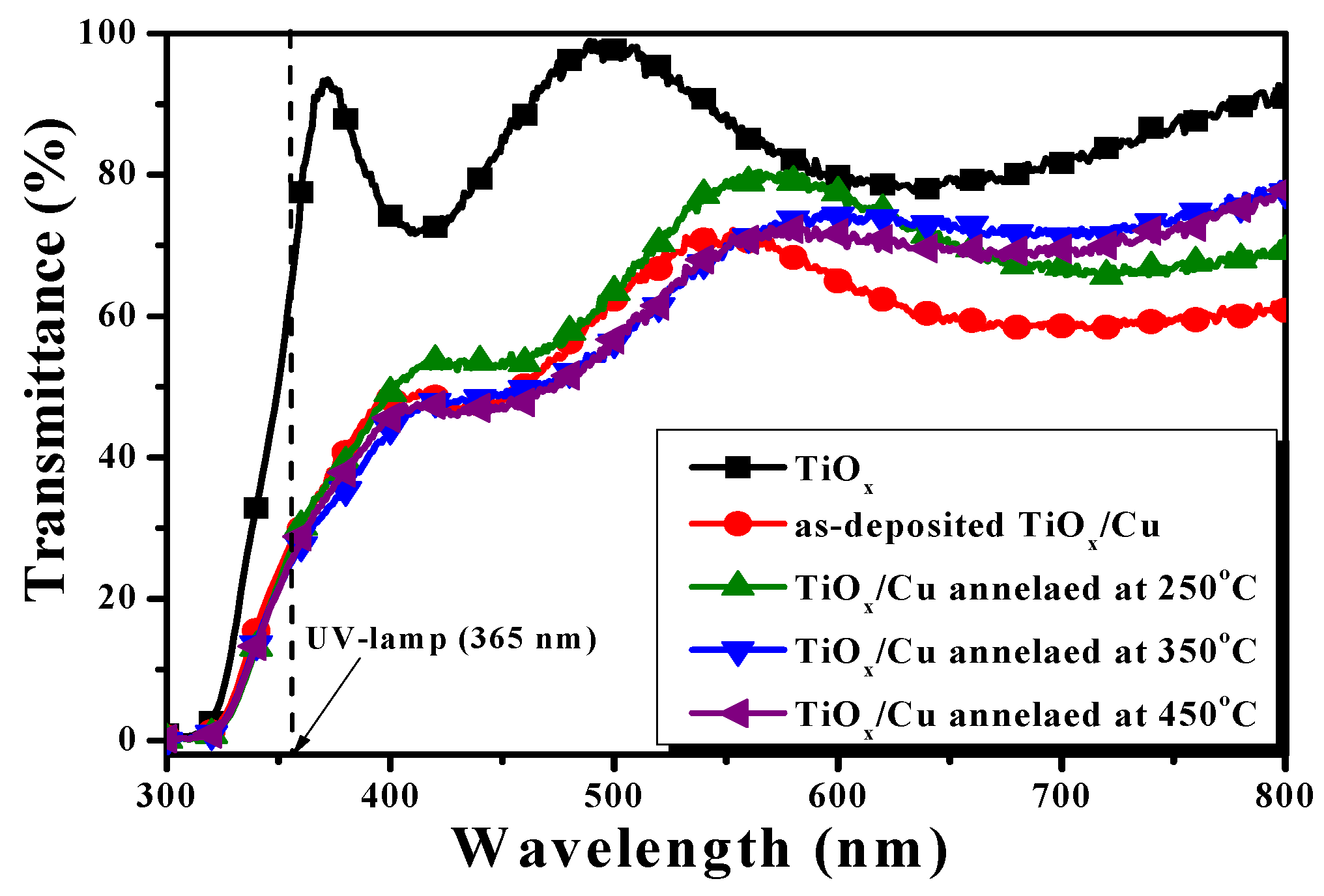
The optical transmittance of the Cu layer deposited onto the TiO
x film and sequentially treated by an RTA process at temperatures of 250 °C, 350 °C, and 450 °C for 1 min under ambient oxygen, as well as the single TiO
x film, are illustrated in
Figure 1. The TiO
x film showed optical transparency, with an average transmittance of about 84% around the visible wavelength (from 400 nm to 700 nm). Beyond the visible wavelength, a drastic decrease in the optical transmittance at the onset of the ultraviolet wavelength (~370 nm) due to the film’s absorption originating from the energy bandgap can be seen. As a 10 nm thick Cu layer deposited onto the TiO
x film, an apparent reduction in the optical transmittance and redshift of the absorption edge was observed. The opaque nature of the Cu metal led to the average transmittance around the visible wavelength decreasing to about 60%. For the TiO
x/Cu structure treated by the RTA process, the average transmittance around the visible wavelengths was somewhat higher than that of the as-deposited TiO
x/Cu structure, while the absorption edge at the UV wavelength of these annealed samples was almost the same as the as-deposited one. This result reveals that the thin metallic Cu and the oxidized Cu layer covered on the TiO
x film both showed a similar obstruct feature as at the visible light, it also occurred in the marked redshift of the absorption edge when compared with that of the single TiO
x film.
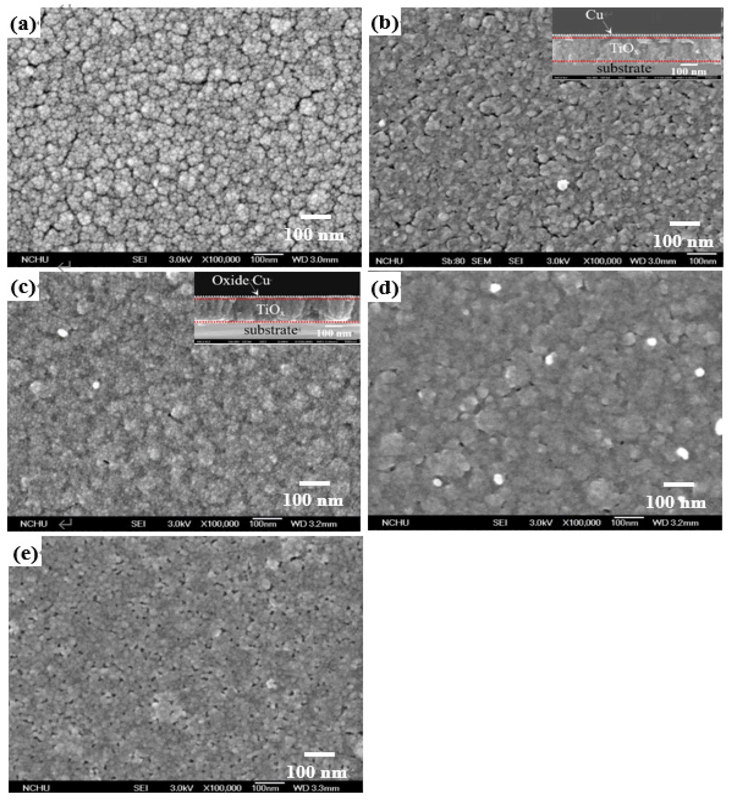
Figure 2a–e respectively show the surface morphologies of the TiO
x film and the TiO
x/Cu structures before and after processing the RTA treatment at temperatures of 250 °C, 350 °C, and 450 °C (the cross-sectional images of the as-deposited and 250 °C-annealed TiO
x/Cu structure are also shown in the inset figures). The surface of the anatase–TiO
x film (
Figure 2a) was uneven, with irregular grains and visible boundaries. Those fine grains distributed over the TiO
x surface became invisible as the film was covered by a 10 nm thick Cu layer (
Figure 2b). The grain boundaries distributed over the surface were then hardly evident, resulting in an ambiguous surface morphology as the TiO
x/Cu structure annealed at 250 °C (
Figure 2c). The surface morphology of the 350 °C-annealed TiO
x/Cu structure (
Figure 2d) became more ambiguous with the appearances of voids and white protrusions. When the annealed temperature reached 450 °C, as shown in
Figure 2e, the voids that might be relevant to the outdiffusion of the oxidized Cu layer were comprehensively distributed over the structural surface. Moreover, although the layered structure could be roughly defined from the inset figures, the change in the microstructures at the TiO
x/Cu interface affected by the annealing process was hardly observed.
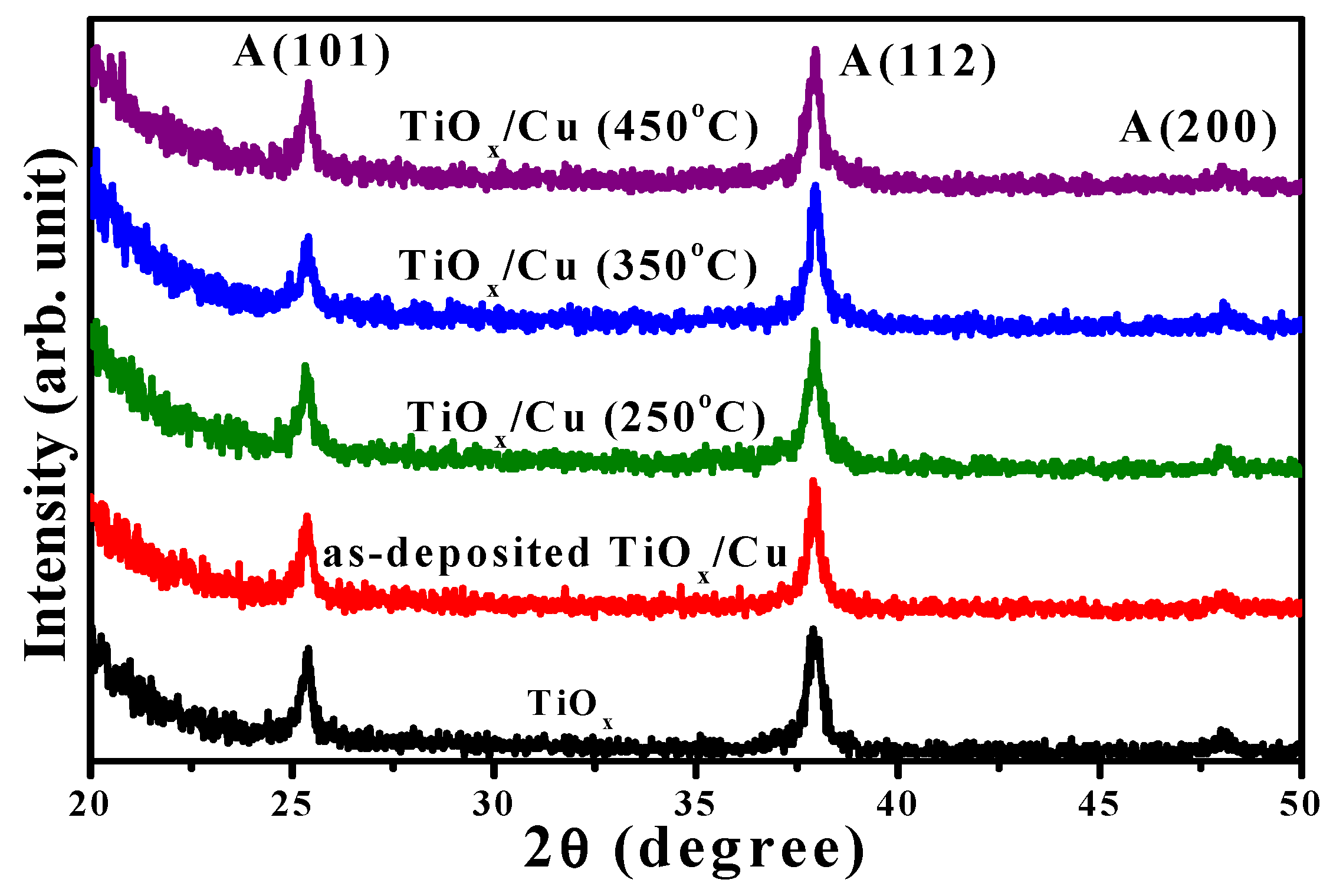
The crystallinity of the as-deposited and annealed TiO
x/Cu structures, as well as the single TiO
x film conducted from the XRD measurements, are presented in
Figure 3. The TiO
x film formed the polycrystal structure with only the anatase phase of the two apparent crystal planes, (hkl), of (101) and (112) and a weak plane of (200) (the diffraction peaks for the anatase phase are taken from the JCPDS No.021-1272 and are marked as “A,” with the crystal plane (hkl) also given). As thin Cu layers coated onto the TiO
x film, the diffraction peaks and their positions associated with different crystal planes of the anatase structure in the XRD spectrum were basically identical to the single TiO
x film. For the TiO
x/Cu structures annealed at temperatures of 250 °C, 350 °C, and 450 °C, the resulting respective XRD patterns still exhibited the anatase phase with dominant crystal planes of (101) and (112). The intensity and position of these two crystal planes were almost identical to that of the single TiO
x film. This result reveals that neither the metallic Cu deposition nor the following oxidation process on the TiO
x/Cu structure affected the crystallinity of the under-layered TiO
x film. Moreover, no clear evidence of the Cu atoms being doped into the TiO
x matrix emerged, as the peak positions of the two anatase planes that appeared in the XRD spectra were basically duplicates of the single TiO
x film. In addition to the investigations on the crystallinity of the under-layered TiO
x film, no featured peaks related to the upper-layered Cu could be identified from these XRD spectra. This might be because the signal related to the metallic Cu and/or its oxidized states was too weak to be observed by the XRD measurements. Accordingly, further observation on the changes of the metallic Cu layer oxidized by the annealing process was essential.
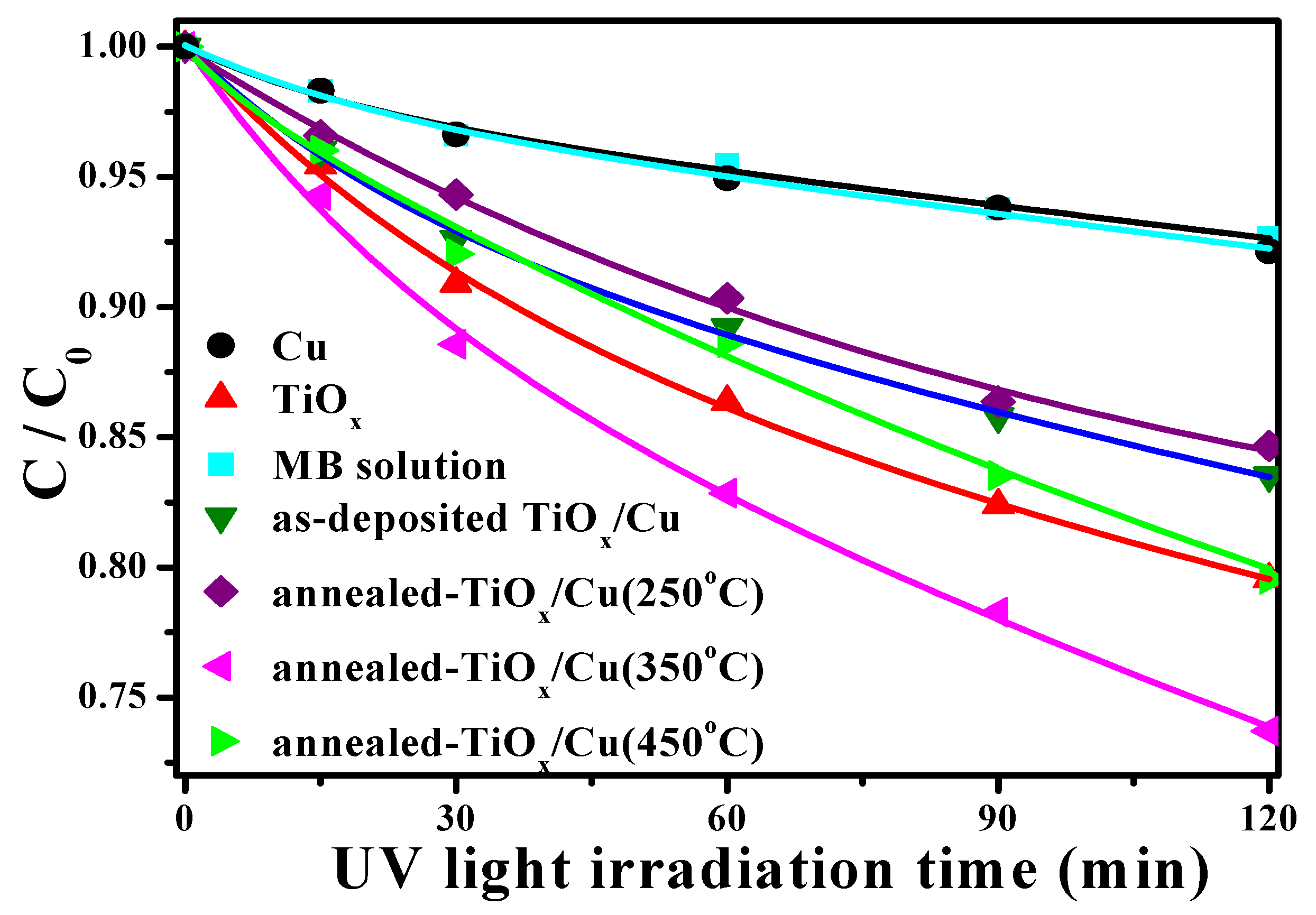
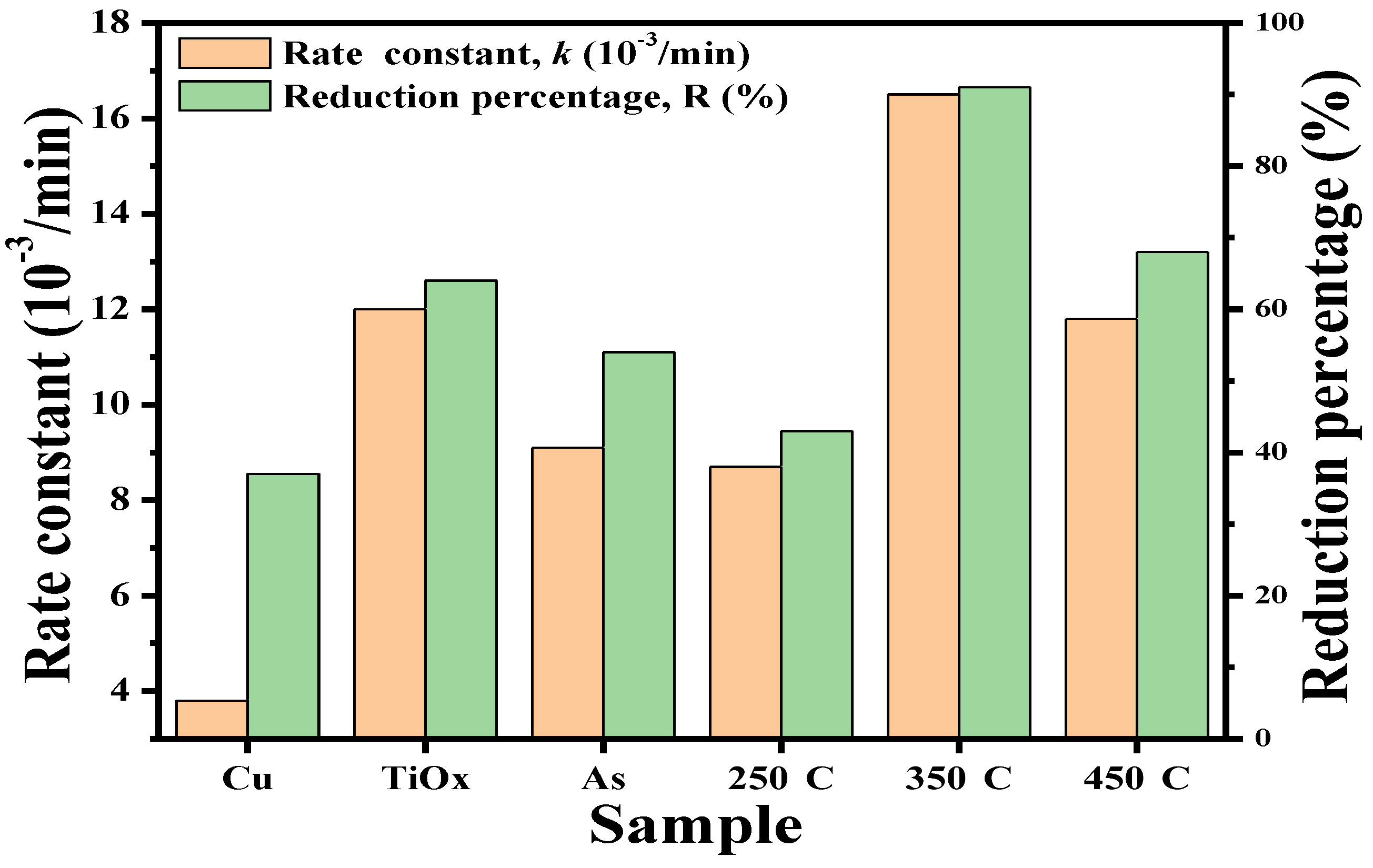
Figure 4 represents the degradation rate associated with the concentration evolution on the MB solution as a function of the UV light irradiation time catalyzed using the single Cu and TiO
x films as well as the as-deposited and annealed TiO
x/Cu structures (the change in the concentration of the MB solution directly irradiated by the UV light is also given as a comparison). According to the limited degradation rate in the MB concentration, as the irradiation time increased, both the MB solution itself and the solution catalyzed by the single 200 nm thick Cu film were only slightly reactive to the UV light illumination. In contrast, the MB solution decomposed by the UV light irradiation, together with the TiO
x film catalyzation, was significantly enhanced, as could be seen in the marked reduction in the concentration rate as the irradiation time increased. As a thin Cu layer covered the TiO
x film, the resulting decomposition efficiency catalyzed by this TiO
x/Cu structure became apparently inferior to the TiO
x film, even when this structure annealed at a temperature of 250 °C. In contrast to the as-deposited and 250 °C-annealed TiO
x/Cu structures, the UV light-induced decomposition to the MB solution incorporating the 350 °C-annealed TiO
x/Cu structure was greatly enhanced, which demonstrates that the degradation rate was clearly faster than that of the MB solution photo-catalyzed only by the TiO
x film. The resulting degradation rate of the MB solution catalyzed using the TiO
x/Cu structure after being annealed at an elevated temperature of 450 °C was again not as good as the degradation rate using the single TiO
x film. The rate constant,
k, which is derived by fitting the concentration evolution of the MB solution under UV light irradiation, complied with the first-order rate equation, which is addressed as the following equation that was employed to quantify the decomposition ability of the MB solution [
28]:
where
C and
Co are the concentrations of the MB solution under UV light irradiation times of
t = 0 and
t, respectively. The rate constant values analyzed from the curves in
Figure 4 are summarized in
Table 1. The decomposition of the MB solution catalyzed by the Cu film under UV light irradiation corresponded to a rate constant (~0.0038 min
−1) similar to the value derived from the MB solution directly decomposed by UV light illumination (~0.0036 min
−1). This decomposition increased markedly to about 0.0120 min
−1 as the solution was photo-decomposed by incorporating the single TiO
x film. The value decreased to about 0.0091 min
−1 as the solution catalyzed when using the TiO
x film covered by a 10 nm thick Cu layer, and a low value of about 0.0087 min
−1 was derived from the degradation rate of the MB solution using the 250 °C-annealed TiO
x/Cu structure. When the TiO
x/Cu structure was annealed at a temperature of 350 °C, the specimen used to photo-decompose the MB solution corresponded to the highest rate constant of about 0.0165 min
−1. It then decreased to about 0.0118 min
−1, as derived from the MB solution photo-decomposed by using the TiO
x/Cu structure annealed at an elevated temperature of 450 °C. This result indicates that the UV-activated degradation rate of the MB solution could be enhanced by more than three times as it was photo-catalyzed using the single TiO
x film. The degradation efficiency of the MB solution could be further improved by about 40% with the assistance of an oxidized Cu layer annealed at 350 °C, while other annealed treatments on the Cu layer showed little support or even obstructed the TiO
x film’s ability to photo-decompose the MB solution.
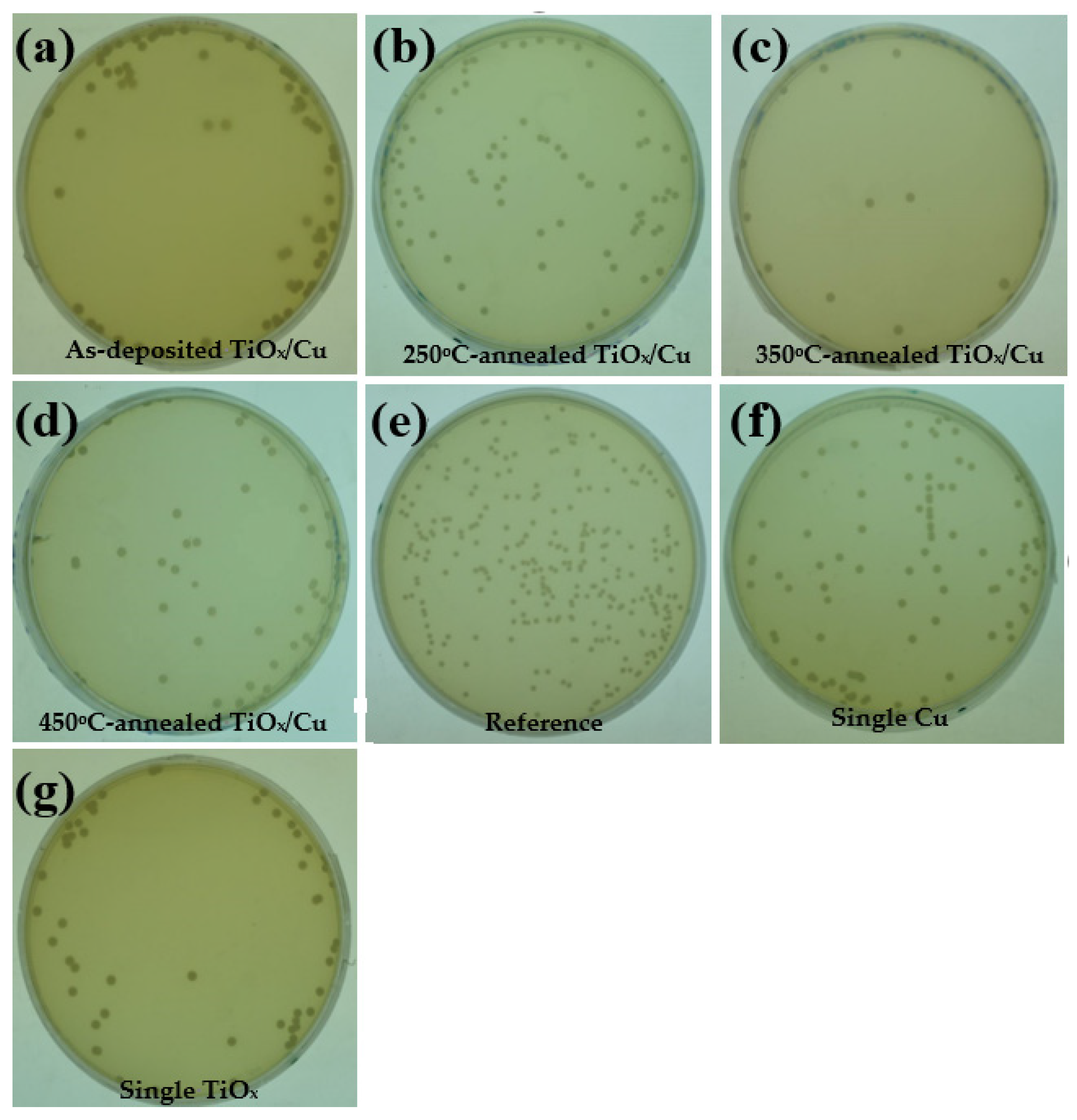
Figure 5a–d respectively show the photographs of the
E. coli bacterial colonies on the nutrient agar after a 24 h incubation period, sterilized using the UV light-activated as-deposited and annealed TiO
x/Cu structures. The photographs of the plate for the
E. coli bacterial colonies that were directly illuminated by the UV light (
Figure 5e, the
E. coli bacterial colonies sterilized using the single Cu (
Figure 5f) and TiO
x (
Figure 5g) films are also given as a comparison). Although the UV-activated Cu film was inactive while decomposing the MB solution, it showed the functional ability to inhibit the growth of the
E. coli bacteria. The number of bacterial colonies counted from the plate (
Figure 5f) decreased to about (87 ± 5.2) × 10
3 CFU/mL, whereas the
E. coli bacteria directly illuminated by the UV light irradiation was about (138 ± 5.5) × 10
3 CFU/mL (
Figure 5e). The growth of the
E. coli bacteria could be further controlled to about (50 ± 4.9) × 10
3 CFU/mL while the Cu film was substituted by the TiO
x film (
Figure 5g). These results indicate that the UV-activated Cu and TiO
x films are both beneficial for suppressing the growth of
E. coli bacteria. When a thin copper layer was coated onto the TiO
x film, the resulting bacterial colonies appearing on the plate, as shown in
Figure 5a, were about (64 ± 4.9) × 10
3 CFU/mL. Although this value is somewhat higher than that of the bacterial colonies using the single TiO
x film, the suppressed efficiency in the growth of the
E. coli bacteria is still apparent when compared with the sterilization using only the single Cu film. Thus, it can be concluded that the under-layered TiO
x film in the TiO
x/Cu structure also played an important part in inhibiting the growth of the
E. coli bacteria. As the TiO
x/Cu structure annealed at a temperature of 250 °C, the growth of the bacterial colonies that appear in
Figure 5b was slightly increased to about (79 ± 5.0) × 10
3 CFU/mL). By contrast, the growth of the bacterial colonies could be minimized to about (12 ± 2.1) × 10
3 CFU/mL, as the
E. coli bacteria were sterilized using the 350 °C-annealed TiO
x/Cu structure (
Figure 5c). An increase in the number of bacterial colonies (~(45 ± 3.5) × 10
3 CFU/mL) was observed from the plate sterilized using the 450 °C-annealed TiO
x/Cu structure (
Figure 5d). The reduction percentage,
R, which quantitatively represents the antibacterial activity of the specimen under UV lamp irradiation, is determined by the evolution of the bacterial colonies on the plate using the following equation [
29]:
where
A is the number of the bacterial colonies counted from the
E. coli directly sterilized by the UV lamp irradiation and
B is the number of the bacterial colonies counted from the plate treated by the specimen incorporation. The higher the reduction percentage, the better the antibacterial activity.
Table 1 summarizes the reduction percentages of the plates shown in
Figure 5. According to this table, the antibacterial activity of the single TiO
x film (~64%) was almost twice as high as the single Cu film (~37%). The degree for the antibacterial activity of the TiO
x film decreased somewhat to about 54% as a semi-opaque Cu layer covered the TiO
x film. The structural activity to sterilize the
E. coli bacterial was continuously deteriorated (~43%) as it was annealed at a temperature of 250 °C. In contrast to the 250 °C-annealed sample, a remarkable increase in antibacterial activity (~91%) was obtained from the TiO
x/Cu structure annealed at a temperature of 350 °C. The antibacterial activity was again decreased to about 68% while the annealed temperature on the TiO
x/Cu structure reached 450 °C. According to the values listed in
Table 1, although the degrees of the rate constant and reduction percentage using the single Cu film were both inferior to those when using the single TiO
x film, the photocatalytic and antibacterial activities for the Cu coated onto the TiO
x film could still be optimized as this structure annealed at a temperature of 350 °C.
Figure 6 depicts the rate constant and reduction percentage of the as-deposited and annealed TiO
x/Cu contact systems as well as the single Cu and TiO
x films listed in
Table 1. The inactive behavior of the single Cu layer and the good photocatalytic activity of the anatase–TiO
x film under UV light irradiation resulted from the formation of the surface hydroxyl radicals that could be clearly seen from the significant difference in the values of their rate constants. However, though the Cu layer was inactive to the UV light irradiation, the metallic Cu showed an ability to inhibit the growth of the
E. coli as a consequence of the bacterial cell being broken by the Cu ion and this ability corresponded to a reduction percentage of 37%. When a thin Cu layer is coated onto the TiO
x film, this structure becomes activable by the UV light irradiation, as observed in the comparison of its rate constant to that of the single Cu layer. However, the shielding effect of the UV light by the surface Cu layer results in an inferior rate constant than the single TiO
x layer. In contrast, the photocatalytic activity induced by the under-layered TiO
x film was found to be beneficial for enhancing the structural antibacterial ability to a value of 54% as compared with that of the single Cu layer. It can also be seen that there was only little change in the rate constant from the 250 °C-annealed TiO
x/Cu structure, while an obvious decrease in the reduction percentage was derived. This reveals that the UV-activated property of this structure was nearly changed, but that the amount of the Cu ions required to break the bacteria had been significantly reduced as a consequence of the oxidation treatment. Both the rate constant and reduction percentage were optimized as the TiO
x/Cu structure was annealed at 350 °C, and these values decreased again when the structure was annealed at a temperature of 450 °C. This suggests that a different mechanism dominated the increase in the photocatalytic activities of these annealed TiO
x/Cu contact systems. As there was neither a change in the crystallinity nor evidence of a new compound or dopant formation in the TiO
x film, the ability of the annealing process on the oxidation of the upper-layered Cu to affect the TiO
x/Cu contact interface might be crucial for determining the structural activities required to decompose the MB solution as well as sterilize the
E. coli bacterial.
With the aim of investigating the annealing process on the changes of the chemical bond configurations, the compositions for the Ti, Cu, and O elements at the contact interface of these TiO
x/Cu structures were examined using XPS measurements through Ar
+ sputtering etching.
Figure 7a–c respectively show the spectra of the binding energies related to the Ti 2p, Cu 2p, and O 1s core levels at the interface of the TiO
x/Cu structure after etching by the Ar
+ sputtering for 60 s. The intensity of the binding energy scales was normalized according to the maximum value in the corresponding XPS spectrum. The Ti 2p
3/2 and Ti 2p
1/2 signal at binding energies of 458.2 and 464.0 eV, respectively, with a difference of 5.8 eV, were measured from the interface of the as-deposited TiO
x/Cu contact system (
Figure 7a). The binding energies and their difference are consistence with the reports on the TiO
2 film with anatase structure, which could be denoted as the bond configuration of Ti(IV) in the spectrum [
1,
30,
31,
32,
33,
34,
35]. When the contact system annealed at a temperature of 250 °C, the Ti 2p
3/2 signal shifted slightly to a lower binding energy of 458.0 eV, with a narrow difference between the signal of the Ti 2p
3/2 and Ti 2p
1/2 (~5.5 eV). This signal shifted clearly to 457.4 eV as the contact system annealed at 450 °C. As quoted from the bond configurations of the Ti species, the shift of the binding energy was ascribed to the appearance of the Ti(III) bond originating from the formation of the oxygen vacancies in the TiO
x film [
5,
36,
37]. It also addresses how the higher the amount of oxygen vacancies that are distributed over the TiO
x film the lower the position of the binding energy of the Ti 2p
3/2 signal. Based on the changes in the binding energy of the Ti 2p
3/2 signal, it could be inferred that the oxygen vacancies distributed over the surface of the TiO
x film gradually increased as the annealing temperature on the structure increased. In the Cu 2p spectra (
Figure 7b), two feature peaks emerged from the Cu 2p
3/2 and Cu 2p
1/2 spin-orbits, with almost the same difference in the binding energy (~19.8 eV), something which could be measured from all of the samples. The binding energy of the Cu 2p
3/2 signal (~932.8 eV) obtained from the as-deposited TiO
x/Cu structure was consistent with the signal measured from the metallic and/or low oxidized Cu states (denoted as Cu(0)/Cu(I) in the spectra) [
38,
39,
40,
41,
42]. As the annealing temperature on this contact system increased, this signal gradually shifted toward a higher binding. The shift of the binding energy is related to the increase in the highly oxidized Cu state (denoted as Cu(II) at about 934.5 eV in this figure), which appeared at the interface of the TiO
x/Cu structure [
40,
41,
42,
43,
44]. This implies that the oxidization of the element Cu in the TiO
x/Cu contact system after the annealing treatment can be traced with XPS analysis, though these Cu-oxidized states were little observed from their corresponding XRD patterns. In addition, the composition of these oxidized Cu states at the TiO
x/Cu contact system could also be estimated by deconvoluting the Cu 2p
3/2 signal into the overlapping peaks related to the Cu (II) and Cu(0)/Cu(I) states. According to the deconvolved area of the Cu(II) and Cu(0)/Cu(I) states, the composition of the highly oxidized state (Cu(II)) at the TiO
x/Cu interface rose from 0.31 to 0.47 and then to 0.71 as the contact structure’s annealing temperature increased from 250 °C to 450 °C. The O 1s signal measured from the interface of the as-deposited TiO
x/Cu structure (
Figure 7c) at about 529.7 eV was correlated to the O-Ti(IV) chemical bond [
5,
32]. As the annealing treatment on the TiO
x/Cu contact system, the O 1s signal became very significant (the original signal is about twice that of the as-deposited sample), revealing that a large number of the Cu atoms had been oxidized and come to dominate the spectra. The binding energies of the O 1s signal shifted from 529.9 eV to 530.1 eV as the annealing temperatures on the TiO
x/Cu structure increased from 250 C to 350 °C. In reference to the reports on the oxidized states of the Cu element, the increase in the formation of the O-Cu(I) chemical bond (~530.4 eV) at the interface of the TiO
x/Cu contact system was responsible for the shift of the binding energy [
34,
41,
45]. It is worth noting that the O 1s signal clearly shifted to a low binding energy of about 529.8 eV as the contact system annealed at a temperature of 450 °C. This result implies that such an annealing treatment would cause the O-Cu(I) oxidized state to evolve into the highly oxidized state that was related to the O-Cu(II) chemical bond (denoted at a binding energy of 529.7 eV in the spectra) [
38,
45]. Incorporating the analysis on the Cu 2p and O 1s core levels, it can be seen that the Cu(0) state’s contact with the TiO
x film predominated over the interface of the as-deposited TiO
x/Cu structure, while this contact gradually evolved into a TiO
x/O-Cu(I) feature as the heterojunction structure oxidation occurred at 250 °C. As the annealed temperature reached 350 °C, more O-Cu(I) states were in contact with the TiO
x film. Eventually, the O-Cu(II) state became the dominant bonding type at the interface of the 450 °C-annealed TiO
x/Cu structure. Based on the investigations of the chemical bond configurations at the interface of these TiO
x/Cu structures, it was confirmed that the nanocomposite TiO
x/Cu
xO heterojunction structure could be realized simply by the annealing treatment. The amount of the Cu element in a highly oxidized state increased with the annealing temperature, while that of the Ti element in the surface of the TiO
x film evolved from a Ti(IV) to a Ti(III) state, revealing that the annealing process not only resulted in the oxidation of the Cu atoms but also caused the outdiffusion of the oxygen atoms from the TiO
x film into the Cu layer. As quoted from the reports, the photo-induced EHP from the Ti(III) oxidized state has also been demonstrated to be separated more effectively than that from the Ti(IV) oxidized state to result in a better photocatalytic activity [
5,
17].
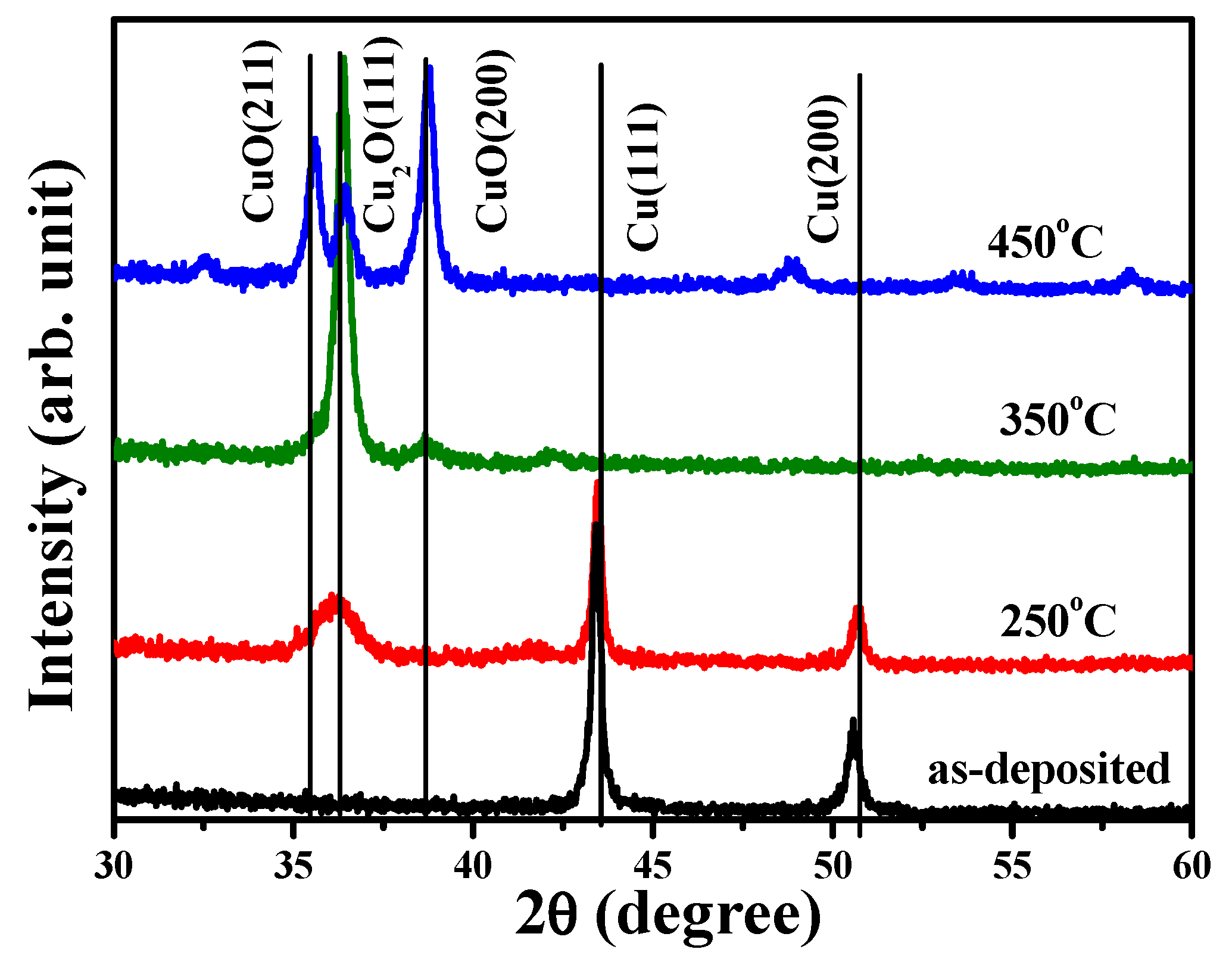
In order to further investigation the crystalline evolution of the single Cu layer affected by the annealing process, 200 nm thick Cu films were directly deposited onto the silicon substrate and processed at annealing temperatures of 250 °C, 350 °C, and 450 °C.
Figure 8 depicts the crystalline evolutions of the as-deposited and annealed Cu films conducted by XRD measurement. The diffraction spectrum of the as-deposited Cu film exhibited only two dominant peaks at about 43.42° and 50.58°, respectively. These peaks could be identified as the face-centered cubic (fcc) structure of the crystal planes (hkl) of (111) and (200) (JCPDS No. 003-1018). As the Cu film annealed at a temperature of 250 °C under ambient oxygen, this thermal oxidation process resulted in another broad peak at about 36.06° other than the crystal planes correspondent with the metallic Cu structure in the XRD spectrum. According to the JCPDS No. 005-0667, this broad peak could be denoted as the oxidized structure of the cuprous oxide phase with the crystal plane (hkl) of (111). This transitionally oxidized Cu phase has also been reported to occur due to the insufficient activation energy between the copper and oxygen atoms [
24,
46,
47]. The Cu
2O(111) crystal plane became the dominant diffraction signal, while those of the crystal planes related to the metallic Cu (Cu(111) and Cu(200)) were absent in the XRD spectrum, as the single Cu film was annealed at 350 °C. In addition, a broad and weak diffraction peak at about 38.66°, identified as the crystal plane belonging to the cupric oxide crystalline phase (denoted as the crystal plane (hkl) of (200), per JCPDS No. 041-0254), also appeared in the XRD spectrum. As referred to in previous reports, the formation of this highly oxidized state of copper was correlated with the adequate thermal activation of copper and oxygen atoms [
46,
48]. This cupric oxide phase, with specific peaks correspondent to the crystal plane (hkl) of (211) and (200), then predominated over the XRD spectrum when the Cu film was annealed at 450 °C. According to the crystalline evolution of the thermally oxidized Cu layer and the chemical bonds of the oxidized Cu states at the interface of the annealed TiO
x/Cu structures, it can be concluded that the metallic copper film was oxidized as the intermediate Cu
2O phase while it was annealed at a low temperature and that the stable CuO phase formed as the metallic Cu layer annealed at an elevated temperature. The results are consistent with previous studies which demonstrate that the appearance of the phases for the oxidized Cu structure is closely related to the annealing temperature and ambient oxygen [
22,
48].
The electrical properties of the single Cu film oxidized at temperatures of 250 °C, 350 °C, and 450 °C are summarized in
Table 2. The as-deposited Cu film possessed high electron carriers of about 2.49 × 10
22 cm
−3, with the mobility of 162 cm
2/V s. A small decrease in electron carriers (~2.07 × 10
22 cm
−3) was measured as the Cu film oxidized at a temperature of 250 °C, which could be attributed to the intermediate Cu
2O phase that was formed in the metallic Cu matrix. The conductive type, converted into
p-type conduction with the hole carriers of about 6.03 × 10
16 cm
−3, was obtained as the Cu film was oxidized at an annealing temperature of 350 °C. This change in the conductive type could be connected to the metallic Cu being completely transformed into the oxidized Cu
2O phase with the limited formation of the CuO phase, both of which have been demonstrated to be
p-type semiconductors [
23,
24,
47,
49,
50]. The structure that developed a composition of Cu
2O and CuO phases as the Cu film oxidized at 450 °C also showed
p-type conduction, with a similar hole concentration of about 3.66 × 10
16 cm
−3. The investigation on the crystalline structure of the oxidized Cu layer suggests that the TiO
x/Cu contact system evolved into the TiO
x/(Cu + Cu
2O) contact system after being annealed at 250 °C under ambient oxygen. A completely oxidized structure constructed from the Cu
2O phase with a little of the CuO phase was subsequently formed and contacted the TiO
x film when the annealed temperature on the structure reached 350 °C. Eventually, the oxidized CuO phase became the dominant structure contacted to the TiO
x film as the contact system annealed at a temperature of 450 °C. Although the conductivity of the anatase–TiO
x film prepared in this study was too low to be measured, it should demonstrate the
n-type conductivity that is associated with the dominated oxygen-vacancy defects in the film [
18,
51,
52]. Accordingly, it could be considered that the as-deposited and 250 °C-annealed TiO
x/Cu contact systems formed a homogeneous heterojunction in
n-type conduction. On the contrary, as
p-type conductivity was measured from the single Cu film annealed at 350 and 450 °C, it can be suggested that the heterojunction structures with the opposite conductivity type (eq.
n-TiO
x/
p-Cu
xO) are formed as the TiO
x/Cu contact system annealed at these two temperatures. Accordingly, an extra electrical field was built at the interfaces of the 350 °C- and 450 °C-annealed TiO
x/Cu structures, which was beneficial for separating the EHPs generated at the contact interface under UV light irradiation. The products of the hydroxyl (·OH) and superoxide anion (·O
2−) radicals originating from the electron and hole carriers, respectively, reacted with the ambient vapor and oxygen and thus could be enhanced due to the inhibition of the recombination of the photo-generated EHPs. As these ·OH and ·O
2− radicals form the primary functional group for catalyzing the decomposition of the organic compounds and for breaking the membrane of the bacteria on the TiO
x surface [
53,
54,
55,
56], the resulting 350 °C- and 450 °C-annealed TiO
x/Cu contact systems that behaved as the
n/p heterojunction structure therefore demonstrated superior activity in decomposing the MB solution and sterilizing the
E. coli, as listed in
Table 1 and
Figure 6.
Except for the built-in voltage established at the interface of the 350 °C- and 450 °C-annealed TiO
x/Cu structure for separating the photo-generated EHPs, the band offset between the anatase–TiO
x and the oxidized Cu states should also be noted, as it was crucial for driving the migration of these photo-generated carriers. The band offset between two materials is established from the discontinuity of the conduction (Δ
Ec) and valence (Δ
Ev) bands originating from the differences in the material’s energy bandgap (
Eg) and electron affinities (
qχ). As quoted from [
23,
24,
49,
57],
p-type Cu
2O and CuO possess the energy bandgaps of about 2.2 eV and 1.7 eV, respectively, with electron affinities of about 3.3 eV and 3.8 eV. Incorporating the energy bandgap (~3.2 eV) and electron affinity (~3.9 eV) of the anatase–TiO
2 phase, the conduction and valence band offsets between the TiO
2 and Cu
2O were 0.6 and 1.6 eV, respectively, while those of the band offsets between the TiO
2 and CuO were 0.1 and 1.6 eV. Thus, the conduction band of the
p-type Cu
2O was more negative than that of the
n-type TiO
2, whereas the band offset of the conduction band between the
p-type CuO and
n-type TiO
2 was relatively invisible. In contrast to the remarked difference in the band offset of the conduction band, the valence band of both the
p-type Cu
2O and CuO possessed almost the same anodic potential, which was less than that of the TiO
2. This result suggests that the electron carriers at the
n-TiO
x/
p-Cu
2O interface in this study, generated under UV light irradiation, would be more prone to migrate to the TiO
x side than that of the carriers generated at the
n-TiO
x/
p-CuO contact system, while a similar driving force appeared to cause the photo-generated hole carriers from the
n-type TiO
x side to the
p-type Cu
2O or CuO interfaces. Thus, the recombination of the EHPs generated under UV light irradiation at the
n-TiO
x/
p-Cu
2O interface would be inhibited more effectively as a result of the
n-TiO
x/
p-Cu
2O structure possessing a superior band offset discontinuity than that of the
n-TiO
x/
p-CuO structure.
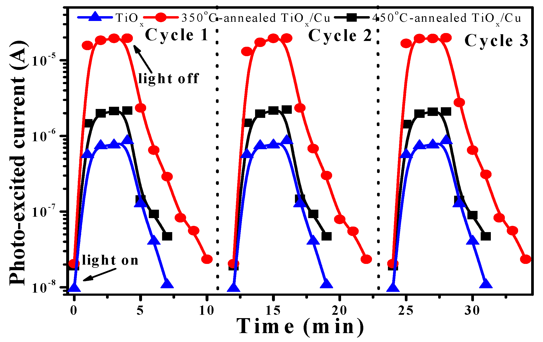
Figure 9 shows three cycles for the response of the photo-excited current as functions of the transient of the 350 °C- and 450 °C-annealed TiO
x/Cu structures as well as the on–off current transient measured from the single TiO
x film. The photo-induced currents of these samples under UV light irradiation are reproducible and reliable, as could be seen from the three cycles’ on–off current transient. The single TiO
x film and the 350 °C- and 450 °C-annealed TiO
x/Cu structures possessed dark currents of about 9.64 × 10
−9 A, 2.05 × 10
−8 A and 1.90 × 10
−8 A, respectively. As the TiO
x film was illuminated by the UV light, the photo-generated carriers increased the current to about 8.62 × 10
−7 A. In contrast to the TiO
x film, a large photo-excited current of approximately 1.96 × 10
−5 A was measured from the 350 °C-annealed TiO
x/Cu sample after being irradiated by the UV light. As the TiO
x/Cu structure was annealed at 450 °C, a photo-induced current of about 2.16 × 10
−6 A was measured. Incorporating the changes in currents of these structures before and after the UV light illumination, the on–off current transient (i.e., the ratio of the photo-excited current to the dark current) of the 450 °C-annealed TiO
x/Cu structure (~113) was somewhat higher than that of the TiO
x film (~89), whereas an apparent increase could be obtained from the on–off current transient of the 350 °C-annealed TiO
x/Cu structure (~953). Based on the above-mentioned investigation, the reason for the increase in the on–off current transient for those two annealed TiO
x/Cu structures was the formation of the
n/p heterojunction, which was helpful for the separation of the photo-generated carriers. Moreover, the way in which the 350 °C-annealed TiO
x/Cu structure possesses a dominant
n-TiO
x/
p-Cu
2O interface with significant band offsets between the conduction and valence bands’ discontinuity could be a critical reason for the corresponding order of magnification that we find on the photo-induced current when compared with the 450 °C-annealed sample. This sample also demonstrated a longer transient time, as determined from the highest photo-excited current to the dark current (7 min), when compared with that of the 450 °C-annealed sample (4 min). Accordingly, the
n-TiO
x/
p-Cu
2O heterojunction predominated over the 350 °C-annealed TiO
x/Cu structure, which significantly enhanced the photo-excited carriers and resulted in a longer carrier lifetime, exhibiting the quality behavior required to decompose the MB solution and inhibit
E. coli growth under UV light irradiation. Based on the mechanism established from this study, the
p-type conduction abundant in the Cu(I) oxidized state (ie. Cu
2O crystalline structure) is essential for improving the photocatalytic activity of the TiO
x/Cu contact system.


