Article

Deposition and Optical Characterization of Sputter Deposited p-Type Delafossite CuGaO2 Thin Films Using Cu2O and Ga2O3 Targets

by
Akash Hari Bharath
*,
Ashwin Kumar Saikumar
and
Kalpathy B. Sundaram
Department of Electrical and Computer Engineering, University of Central Florida, Orlando, FL 32826, USA
*
Author to whom correspondence should be addressed.
Materials 2024, 17(7), 1609; https://doi.org/10.3390/ma17071609
Submission received: 6 March 2024 / Revised: 20 March 2024 / Accepted: 31 March 2024 / Published: 1 April 2024
(This article belongs to the Special Issue Advanced Semiconductor/Memory Materials and Devices)

Abstract

:
CuGaO2 thin films were deposited using the RF magnetron sputtering technique using Cu2O and Ga2O3 targets. The films were deposited at room temperature onto a quartz slide. The sputtering power of Cu2O remained constant at 50 W, while the sputtering power of Ga2O3 was systematically varied from 150 W to 200 W. The films were subsequently subjected to annealing at temperatures of 850 °C and 900 °C in a nitrogen atmosphere for a duration of 5 h. XRD analysis on films deposited with a Ga2O3 sputtering power of 175 W annealed at 900 °C revealed the development of nearly single-phase delafossite CuGaO2 thin films. SEM images of films annealed at 900 °C showed an increasing trend in grain size with a change in sputtering power level. Optical studies performed on the film revealed a transmission of 84.97% and indicated a band gap of approximately 3.27 eV. The film exhibited a refractive index of 2.5 within the wavelength range of 300 to 450 nm.

1. Introduction

Transparent conducting oxides (TCOs) represent a distinct category of compounds distinguished by their notable optical transparency in the visible spectrum, coupled with excellent electrical conductivity [1]. As a result of these characteristics, TCOs find extensive applications across various optical devices, including light-emitting diodes, solar cells, sensors, and displays [2,3,4,5]. P-type and n-type TCOs can be potentially used in touch panels in hospitals and smartphones [6]. In this family of p-type TCOs, CuCrO2 is known to have antibacterial properties. Further, these antibacterial properties may find applications in biomedical implants, as reported by Jabed et al. in metallic glass-based materials [7]. TCOs are achieved by doping metal oxides by adding more charge carriers while essentially maintaining their optical characteristics. Due to high conductivity, n-type TCOs are used for conducting electrode applications [8]. Extensive research has been conducted on n-type TCOs such as Sn-doped In2O3 (ITO) [9,10], Sc-doped ZnO [11,12], and Al-doped ZnO (AZO) [13,14,15,16]. Nonetheless, there exists a lack of research on p-type TCOs, impeding the progress of transparent electronics applications [17,18,19]. In the case of p-type TCOs, it is difficult to synthesize a film that has both good optical transparency and high electrical conductivity.
The challenge in achieving a p-type TCO is due to the deep localization of holes at the O-2p oxygen level. This can be explained by the fact that the valence orbits of metallic atoms are located at a much higher energy level than O-2p levels [20,21]. Studies show that metal oxides have far lower valance band levels than metals. Doping offers a potential solution to this issue [22]. Nonetheless, the existence of highly electronegative O2 ions hinders the mobility of holes within the crystal lattice. To mitigate holes inside the crystal lattice, the localized holes would require a high amount of energy to overcome the large barrier height [23]. This is one of the main reasons why p-type TCOs have low electrical conductivity [24,25]. Hosono et al. introduced the idea of chemical modulation of the valence band (CMVB) as a solution to this problem [20]. It was discovered that incorporating cations like Cu+ results in the formation of a strong covalent bond with oxygen ions. This is because the energy difference between O 2p6 and Cu 3d10 is very small and Cu 3d10 forms a strong covalent bond with the O 2p6. As a result, the energy level of O-2p increases, leading to a decrease in the coulombic attraction between O2 ions and the holes. This increases conductivity by allowing holes to flow freely across the crystal lattice [22]. The optical transparency would be preserved due to the closed shell nature of Cu 3d10 which prevents coloration [25].
Films synthesized using the CMVB concept are called delafossites. The cation used for this process could be Cu+ or Ag+. Earlier research shows that the film made with Ag+ cation has very high electrical resistivity (104–106 Ω-cm) [25]. This is due to the exceptionally low carrier mobility resulting from the unfavorable energy alignment between O-p and Ag-4d levels [26]. Delafossite compounds incorporating Cu+ cations are referred to as Cu-based delafossites. Copper-based delafossites are gaining a lot of attention due to their large bandgap [19,27]. Cu-based delafossite materials are represented by the chemical formula CuMO2, with Cu denoting the positively charged monovalent cation (Cu+), M representing trivalent cations such as Cr3+, Ga3+, and Y3+, and oxygen serving as the negatively charged divalent anion (O2−). CuGaO2 belongs to the Cu-based delafossite family and is being researched extensively because of its electrical, optical, and photovoltaic properties [28,29,30]. Additionally, they could also be used for maintaining energy through solar water splitting, fuel cells, battery devices, and electrolyzers [31]. It has a high bandgap along with demonstrating excellent optical transparency and high hole mobility [32,33,34]. Numerous methods have been used to deposit p-type CuGaO2 films. The sol-gel deposition process performed by Ehara et al. uses copper nitrate trihydrate and gallium nitrate n-hydrate dissolved in 2-methoxyethanol [35]. Yu et al. performed a hydrothermal process to obtain delafossite CuGaO2. In this process, the precursor was prepared by dissolving copper and gallium nitrate in water with pH adjusted by adding potassium hydroxide. They are able to achieve delafossite CuGaO2 phase in a temperature range of 170–240 °C [34]. Tsay et al. utilized the spin coating technique, where they prepared the precursor solution by dissolving copper acetate monohydrate and gallium nitrate hydrate in 2-methoxyethanol. Subsequently, the precursor underwent spin coating at a rate of 1500 rpm for 30 s and was annealed at 900 °C for 1 h [36]. The pulsed laser deposition process conducted by Ueda et al. uses a Cu2O and Ga2O3 powder-pressed target. The target is eroded using a KrF excimer laser with a laser frequency of 20 Hz [37].
RF magnetron sputtering provides the flexibility to choose target materials across a wide spectrum of melting points. It also gives us the freedom to control the ratio of the material by adjusting the sputtering power of different targets. Furthermore, the RF magnetron sputtering technique gives excellent adhesion across a large surface area without requiring the use of hazardous or specialized precursors, which are necessary for CVD [38]. Delafossite CuGaO2 can be obtained by various sputtering methods like reactive sputtering of Cu/Ga target with O2 gas [39], CuO/Ga2O3 single target sputtering [27], and dual sputtering using Cu and Ga2O3 targets [8].
In this work, CuGaO2 thin films were deposited for the first time using the RF sputtering technique with Cu2O and Ga2O3 targets. This technique allows the freedom to select various sputtering power levels for the two targets to achieve the right composition. The sputtering power of the Cu2O was kept constant, and the Ga2O3 sputtering power was varied. The films were deposited at room temperature and then annealed in a N2 atmosphere. The process was optimized to obtain the delafossite phase. The structural, morphological, and optical properties of the synthesized CuGaO2 thin films were then studied.

2. Experimental

2.1. Deposition of CuGaO2 Thin Films

The CuGaO2 thin films used in this work were deposited using an AJA international ultra-high vacuum three-gun sputtering system. The dual targets used were 3-inch diameter of Cu2O (99.99% purity, Maideli Advanced Materials Co., Ltd., Jiangyin, China) and Ga2O3 (99.99% purity, Maideli Advanced Materials Co., Ltd., Jiangyin, China). The frequency of the RF magnetron sources for both targets was of 13.56 MHz. Fused quartz slides were used as substrates for depositing the films. The substrates were cleaned using acetone, methanol, and deionized water and blow-dried using nitrogen gas before the deposition. A base pressure of 5 × 10⁻⁷ Torr was achieved before starting the deposition. Ultra-high purity argon gas at a flow rate of 10 sccm was used as the sputtering gas. The power applied to the Cu2O target was kept constant at 50 W, while the power applied to the Ga2O3 target was varied between 150 and 200 W. Based on the deposition rates at different power levels, the thicknesses of the films maintained were around 2000 Å. To ensure a uniform film thickness, the substrate holder was rotated at a speed of 20 rpm. Post-deposition annealing of the films were carried out in a tube furnace at 850 °C and 900 °C. The annealing was performed for 5 h in the presence of ultra-high-purity N2 ambiance at a constant flow of 300 sccm. Table 1 lists the deposition parameters that were used for this work. All the data presented were verified by preparing several samples under identical conditions.

2.2. Film Characterization

The thicknesses of the deposited films were measured using a Veeco Dektak 150 surface profilometer (Veeco, Plainview, NY, USA). XRD analysis was performed using the PANalytical Empyrean XRD system (Malvern Panalytical, Westborough, MA, USA), using a Cu radiation source at 45 kV and 40 mA. The diffraction patterns were recorded at 2θ angles of 25°–70°. HighScore Plus software version 4.5 (Malvern Panalytical, Westborough, MA, USA) was used to analyze the phase information. The film’s composition was analyzed using ESCALAB 250 Xi + X-ray photoelectron spectroscopy (XPS) (ThermoFisher Scientific, Waltham, MA, USA) with a monochromatic source Al Kα source (1486.7 eV). Before XPS measurements, an inbuild EX06 ion source was used to perform ion milling on the sample to remove the surface oxygen. The XPS data were then analyzed using Thermo Fischer Scientific Avantage software (version 5.9902) to perform XPS peak fitting. Surface morphological studies of the films were performed using the Zeiss Ultra-55 SEM (Zeiss Microscopy, White Plains, NY, USA). Optical transmission analysis was performed at light wavelengths ranging from 300 to 800 nm using a Cary 100 UV-Vis spectrometer (Varian Analytical Instruments, Walnut Creek, CA, USA). The Tauc plot method was used to calculate the bandgap of the films. The conductivity type of the post-deposition-annealed film was found using the hot probe method.

3. Results and Discussion

3.1. XRD and XPS Analysis

The XRD diffractograms of films deposited at various Ga2O3 sputtering powers (150 W, 175 W, and 200 W) and subjected to annealing at 850 °C are shown in Figure 1. The 2θ range was adjusted to eliminate the quartz amorphous peak that was observed in all films at the range between 18° and 25°. The as-deposited film did not show any diffraction peaks and confirmed to be amorphous in nature. However, all the annealed films were found to be nanocrystalline due to their distinct diffraction peaks. The lack of discernible peaks in the as-deposited films can be explained by the insufficient energy present during the deposition process, hindering crystallization. Similar to the research reported by Dong L et al. [40], distinct Ga2O3 peaks were identified at 30.22° on all the annealed thin films. Figure 1 shows the XRD diffractograms of the aforementioned films were annealed at 850 °C. As observed in Figure 1, films deposited using a sputtering power of 150 W for Ga2O3 exhibited peaks associated with spinel CuGa2O4, alongside a CuO peak detected at 54.3°. By increasing the sputtering power to 175 W, the CuO peak was no longer visible, and the remaining CuGa2O4 peaks became stronger. However, by increasing the Ga2O3 sputtering power to 200 W, peaks pertaining to CuGa2O4 started to disappear, while peaks pertaining to CuGaO2 started to appear. The films mentioned above were further not characterized due to the absence of CuGaO2 phase films.
Figure 2 shows XRD results of films annealed at 900 °C. Raising the annealing temperature to 900 °C resulted in the disappearance of peaks associated with CuGa2O4 while peaks pertaining to CuGaO2 emerged. Similar results were reported in earlier studies [27,41]. The films deposited at 150 W Ga2O3 power showed a combination of CuO, Ga2O3, and CuGaO2 peaks. With the increase in Ga2O3 sputtering power to 175 W, the peaks pertaining to CuO disappeared. This phenomenon can be attributed to the rise in Ga2O3 concentration within the film as the sputtering power for Ga2O3 increases, potentially facilitating its reaction with CuO to yield CuGaO2. With the exception of Ga2O3 peak at 30.22°, nearly single-phase CuGaO2 was identified. However, when the Ga2O3 sputtering power was increased to 200 W, the predominantly single-phase CuGaO2 diminished, while additional Ga2O3 peaks started emerging, attributable to the heightened Ga concentration within the film. No peaks associated with spinel CuGa2O4 were detected, when the films were annealed at 900 °C. In the film deposited with 175 W power to the Ga2O3 target, the major peaks were identified at 2θ angles of 31.4°, 35.21°, 36.43°, 41.06°, and 62.59° indexed to (006), (101), (012), (105), and (110), respectively. This shows the formation of nearly single-phase delafossite CuGaO2 (JCPDS PDF # 41–0255). These findings indicate that the CuGaO2 phase was achieved at relatively high temperatures compared to CuO and CuGa2O4 phases at low temperatures. The findings from the XRD analysis are summarized in Table 2, Table 3, Table 4, Table 5 and Table 6. Equation (1) explains the chemical reaction for the formation of CuGaO2 [39].
CuGa2O4 + CuO → 2CuGaO2 + 0.5O2
As the optimal performance was achieved by sputtering the film with a Ga2O3 sputtering power of 175 W and subsequently annealing it at 900 °C, and XPS analysis was only conducted on these films. Figure 3a shows the XPS survey spectra pertaining to the film. It was confirmed from the survey spectrum that only Cu, Ga, and O-related peaks were found. Figure 3b shows two peaks denoting Cu 2p3/2 and Cu 2p1/2 detected at binding energies of 932.13 eV and 951.93 eV, respectively. The lack of satellite peaks within the range of 940 and 950 eV served as a confirmation of the absence of Cu2+ species. Figure 3c shows the Ga 2p3/2 peak observed at 1117.09 eV. Two sub-peaks were found for the O 1s state at 530.07 eV and 531.6 eV, as seen in Figure 3d. The peak detected at a binding energy of 530.07 eV is indicative of lattice oxygen within CuGaO2, whereas the peak observed at 531.6 eV corresponds to chemisorbed oxygen. The peaks found at its associated binding energy are consistent with those in other reported researches [29,42].

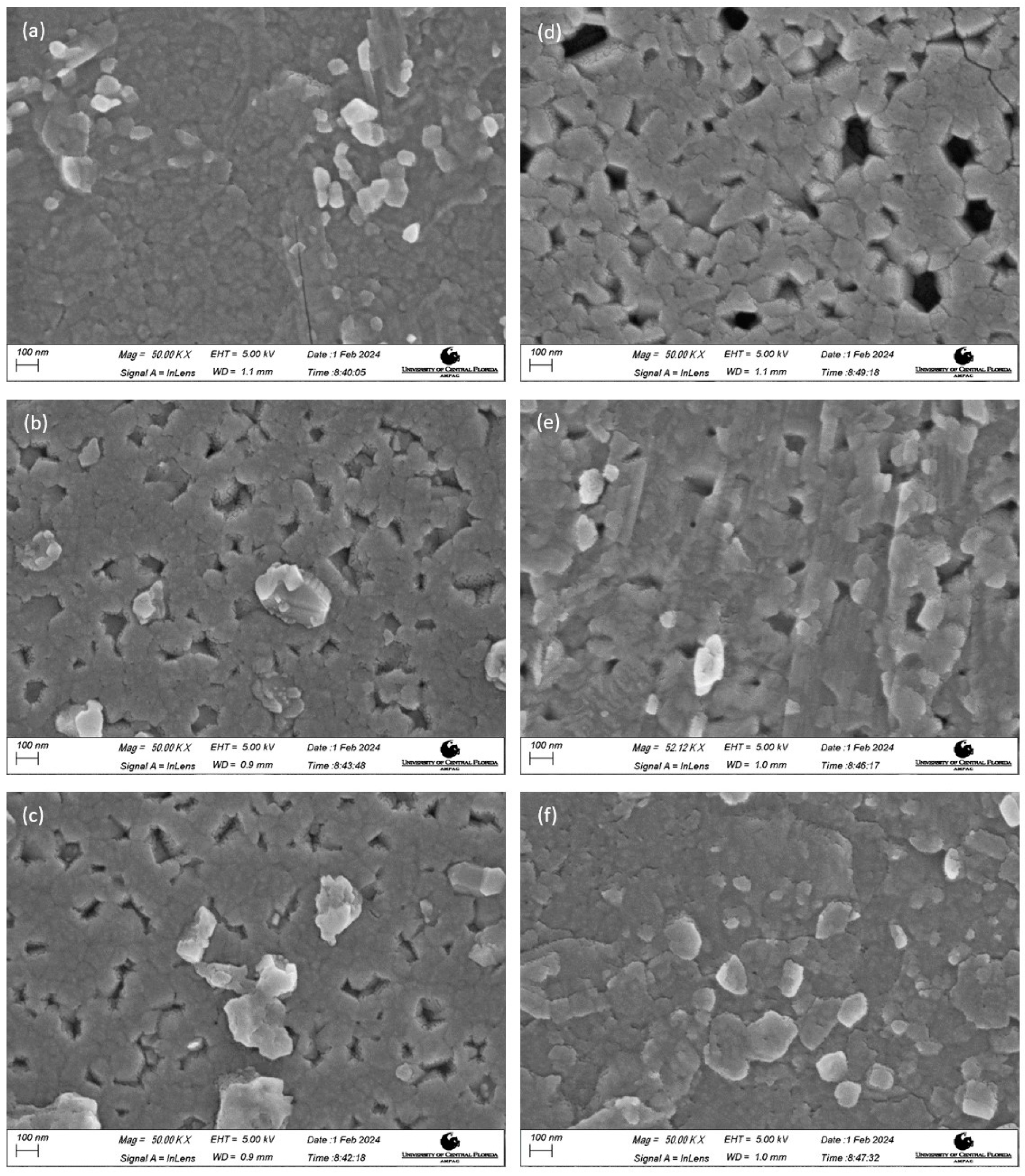
3.2. Morphology Studies

SEM images of the post-deposition-annealed films are shown in Figure 4. All the images were obtained at a 50 K magnification. Distinct grains were seen on all the films, confirming their nano-crystallinity as previously reported in the XRD section. Figure 4a–c shows the films annealed at 850 °C, and Figure 4d–f show the films annealed at 900 °C. Overall, it was observed that an increase in annealing temperature led to an increase in the grain size of the films, as reported by [41,43].

3.3. Optical Studies

3.3.1. Optical Transmission

Optical transmission analyses were performed on all films deposited onto quartz slides following annealing. UV-Vis spectrophotometry recorded transmission data ranging from 200 to 800 nm. Figure 5 illustrates the optical transmissions of films post-deposition-annealed at 850 °C and 900 °C. Films annealed at 850 °C displayed a rising trend in optical transmission with the increasing sputtering power. The films deposited with Ga2O3 sputtering powers of 150 W, 175 W, and 200 W had optical transmissions of 77.15%, 82.45%, and 84.14%, respectively. However, films subjected to annealing at 900 °C exhibited a decrease in transmission, as the sputtering power increased. The films deposited with Ga2O3 sputtering powers of 150 W, 175 W, and 200 W had optical transmissions of 85.03%, 84.97%, and 82.37%, respectively. The increase and the decrease in the optical transmission perfectly aligned with the grain size change reported in the morphology studies section. As the grain size decreased, the optical transmission was identified to increase in the films annealed at 850 °C. On the contrary, the films annealed at 900 °C showed an opposite trend of reduction in optical transmission with an increase in grain size. From SEM data, we could conclude that with an increase in grain size, the optical transmission decreased. A similar correlation between optical transmission and grain size has been reported in [44,45].

3.3.2. Optical Bandgap

The optical bandgap of CuGaO2 thin films subjected to post-deposition annealing, was determined using the Tauc plot method [46]. The absorption coefficient (α) was calculated based on the transmission spectra data using the equation:
α = 2.303 t log 10 ( % T )
where t represents the thickness of the CuGaO2 thin film, and T denotes the transmission of the film.
The Tauc equation was used to find the bandgap based on the absorption coefficient:
α h ν 1 n = B ( h ν E g )
where “n” indicates the nature of sample transition, “h” is the photon energy, “ ν ” is the vibration frequency, “ h ν ” is the Planck’s constant, Eg denotes the optical bandgap, and B is constant. The values of n equal ½ for direct allowed, 2 for indirect allowed, and 3/2 for direct forbidden transitions [46,47]. Since n = ½ yielded the best linear fit of the α h ν 1 n vs. the photon energy curve, the films deposited in this study show a direct bandgap transition. This is also backed by previous research on this material [37,39]. The bandgap values were determined by extrapolating the linear portion of the curves to the x-axis.
Figure 6 illustrates the Tauc plots for films subjected to annealing temperatures of 850 °C and 900 °C. For films deposited using Ga2O3 sputtering powers of 150 W, 175 W, and 200 W and annealed at 850 °C, the corresponding optical bandgaps were measured to be 3.45 eV, 3.39 eV, and 3.4 eV, respectively. Similarly, films deposited under the same power settings and annealed at 900 °C exhibited optical bandgaps of 3.54 eV, 3.27 eV, and 3.5 eV, respectively. As seen in the XRD results in Figure 2, the films deposited with Ga2O3 powers of 150 W and 200 W had a higher Ga2O3 content, which is known to have a higher bandgap than CuGaO2. The decrease in the bandgap of the 175 W film can be attributed to the fact that it was nearly single-phase CuGaO2, which closely matches other reported results [48]. Copper-based delafossites like CuGaO2, CuCrO2, and CuInO2 are known to exhibit p-type conductivity owing to its intrinsic defects such as interstitial oxygen ions and/or Cu vacancies in the copper lattice [49,50]. This was further verified using the hot probe test on all the films showing p-type behavior.

3.3.3. Refractive Index Studies of CuGaO2

The refractive index of the nearly single-phase CuGaO2 thin film was determined utilizing the following formula [51]:
1 2 η t = 1 λ m + 1 1 λ m
where η represents the refractive index of the CuGaO2 film, t indicates the thickness of the film, and λm+1 and λm denote the wavelengths where the successive maxima are observed in the transmission spectrum. The refractive index of the CuGaO2 thin film was found to be 2.5 in the 300–450 nm wavelength range which is similar to the previously reported data [52].

4. Conclusions

In this study, thin films of CuGaO2 were successfully deposited through a dual sputtering method utilizing Cu2O and Ga2O3 targets. These films were deposited on a quartz substrate, maintaining the Cu2O sputtering power at a constant 50 W while varying the Ga2O3 power. Subsequently, the samples underwent annealing at temperatures of 850 °C and 900 °C in a N2 atmosphere, followed by analysis of their structural and optical characteristics using XRD, XPS, SEM, and UV-Vis spectroscopy. When annealed at 900 °C, the films deposited at a Ga2O3 sputtering power of 150 W showed the presence of CuO, and the films deposited with a sputtering power of 200 W were Ga2O3 phase-rich. Nearly single-phase delafossite CuGaO2 films were obtained with a Ga2O3 sputtering power of 175 W. CuGa2O4 peaks were observed, when the film was annealed at 850 °C. SEM images revealed an increasing trend in grain size when annealed at 850 °C and a decrease in grain size when annealed at 900 °C. The optical transmission of the film increased with the decrease in grain size. The nearly single-phase CuGaO2 film had an optical transmission of about 85% at the visible range, and its optical bandgap was found to be 3.27 eV. The refractive index of the film was found to be 2.5 in the 300–450 nm wavelength range.

Author Contributions

Conceptualization, K.B.S.; Methodology, A.H.B. and K.B.S.; Validation, A.H.B.; Formal analysis, A.H.B.; Investigation, A.H.B.; Data curation, A.H.B.; Writing—original draft, A.H.B.; Writing—review & editing, A.K.S. and K.B.S.; Visualization, A.H.B.; Supervision, A.K.S. and K.B.S. All authors have read and agreed to the published version of the manuscript.

Funding

This research received no external funding.

Institutional Review Board Statement

Not applicable.

Informed Consent Statement

Not applicable.

Data Availability Statement

Data are contained within the article.

Acknowledgments

The authors would like to acknowledge the NSF MRI: ECCS: 1726636 and MCF-AMPAC facility, MSE, and CECS for the XPS use.

Conflicts of Interest

The authors declare no conflict of interest.

References

  1. Hu, L.; Wei, R.H.; Tang, X.W.; Lu, W.J.; Zhu, X.B.; Sun, Y.P. Design strategy for p-type transparent conducting oxides. J. Appl. Phys. 2020, 128, 140902. [Google Scholar] [CrossRef]
  2. Stadler, A. Transparent Conducting Oxides-An Up-to-Date Overview. Materials 2012, 5, 661–683. [Google Scholar] [CrossRef]
  3. Lan, J.-H.; Kanicki, J.; Catalano, A.; Keane, J.; Boer, W.d.; Gu, T. Patterning of transparent conducting oxide thin films by wet etching for a-Si:H TFT-LCDs. J. Electron. Mater. 1996, 25, 1806–1817. [Google Scholar] [CrossRef]
  4. Saikumar, A.K.; Nehate, S.D.; Sundaram, K.B. Review—RF Sputtered Films of Ga2O3. ECS J. Solid State Sci. Technol. 2019, 8, Q3064. [Google Scholar] [CrossRef]
  5. Nehate, S.; Saikumar, A.K.; Sundaram, K.B. A review of recent developments in aluminum gallium oxide thin films and devices. Crit. Rev. Solid State Mater. Sci. 2022, 47, 538–569. [Google Scholar] [CrossRef]
  6. Chiu, T.-W.; Yang, Y.-C.; Yeh, A.-C.; Wang, Y.-P.; Feng, Y.-W. Antibacterial property of CuCrO2 thin films prepared by RF magnetron sputtering deposition. Vacuum 2013, 87, 174–177. [Google Scholar] [CrossRef]
  7. Jabed, A.; Rahman, Z.U.; Khan, M.M.; Haider, W.; Shabib, I. Combinatorial development and in vitro characterization of the quaternary Zr–Ti–X–Y (X–Y = Cu–Ag/Co–Ni) metallic glass for prospective bioimplants. Adv. Eng. Mater. 2019, 21, 1900726. [Google Scholar] [CrossRef]
  8. Saikumar, A.K.; Sundaresh, S.; Sundaram, K.B. Preparation and characterization of p-type copper gallium oxide (CuGaO2) thin films by dual sputtering using Cu and Ga2O3 targets. ECS J. Solid State Sci. Technol. 2022, 11, 065010. [Google Scholar] [CrossRef]
  9. Fallah, H.R.; Ghasemi, M.; Hassanzadeh, A.; Steki, H. The effect of annealing on structural, electrical and optical properties of nanostructured ITO films prepared by e-beam evaporation. Mater. Res. Bull. 2007, 42, 487–496. [Google Scholar] [CrossRef]
  10. George, J.; Menon, C.S. Electrical and optical properties of electron beam evaporated ITO thin films. Surf. Coat. Technol. 2000, 132, 45–48. [Google Scholar] [CrossRef]
  11. Dixon, S.C.; Sathasivam, S.; Williamson, B.A.D.; Scanlon, D.O.; Carmalt, C.J.; Parkin, I.P. Transparent conducting n-type ZnO:Sc—Synthesis, optoelectronic properties and theoretical insight. J. Mater. Chem. C 2017, 5, 7585–7597. [Google Scholar] [CrossRef]
  12. Samadi, M.; Zirak, M.; Naseri, A.; Khorashadizade, E.; Moshfegh, A.Z. Recent progress on doped ZnO nanostructures for visible-light photocatalysis. Thin Solid Film. 2016, 605, 2–19. [Google Scholar] [CrossRef]
  13. Shan, F.; Yu, Y.s. Band gap energy of pure and Al-doped ZnO thin films. J. Eur. Ceram. Soc. 2004, 24, 1869–1872. [Google Scholar] [CrossRef]
  14. Maldonado, F.; Stashans, A. Al-doped ZnO: Electronic, electrical and structural properties. J. Phys. Chem. Solids 2010, 71, 784–787. [Google Scholar] [CrossRef]
  15. Phelps, J.R.; Saikumar, A.K.; Abdolvand, R.; Sundaram, K.B. Comparison of RF and High Impulse Magnetron Sputtered Gallium-Doped Zinc Oxide Thin Films. Coatings 2023, 13, 71. [Google Scholar] [CrossRef]
  16. Shantheyanda, B.P.; Sundaram, K.B.; Shiradkar, N.S. Studies on the effect of hydrogen doping during deposition of Al: ZnO films using RF magnetron sputtering. Mater. Sci. Eng. B 2012, 177, 1777–1782. [Google Scholar] [CrossRef]
  17. Sundaresh, S.; Bharath, A.H.; Sundaram, K.B. Synthesis and Characterization of Radio-Frequency-Sputtered Delafossite Copper Indium Oxide (CuInO2) Thin Films. ECS J. Solid State Sci. Technol. 2023, 12, 043010. [Google Scholar] [CrossRef]
  18. Sundaresh, S.; Bharath, A.H.; Sundaram, K.B. Effect of Annealing Temperature on Radio Frequency Sputtered p-Type Delafossite Copper Chromium Oxide (CuCrO2) Thin Films and Investigation of Diode Characteristics Forming Transparent pn-Heterojunction. Coatings 2023, 13, 263. [Google Scholar] [CrossRef]
  19. Sundaresh, S.; Bharath, A.H.; Sundaram, K.B. Effect of Cu2O Sputtering Power Variation on the Characteristics of Radio Frequency Sputtered p-Type Delafossite CuCrO2 Thin Films. Coatings 2023, 13, 395. [Google Scholar] [CrossRef]
  20. Kawazoe, H.; Yasukawa, M.; Hyodo, H.; Kurita, M.; Yanagi, H.; Hosono, H. P-type electrical conduction in transparent thin films of CuAlO2. Nature 1997, 389, 939–942. [Google Scholar] [CrossRef]
  21. Hautier, G.; Miglio, A.; Ceder, G.; Rignanese, G.-M.; Gonze, X. Identification and design principles of low hole effective mass p-type transparent conducting oxides. Nat. Commun. 2013, 4, 2292. [Google Scholar] [CrossRef]
  22. Banerjee, A.N.; Chattopadhyay, K.K. Recent developments in the emerging field of crystalline p-type transparent conducting oxide thin films. Prog. Cryst. Growth Charact. Mater. 2005, 50, 52–105. [Google Scholar] [CrossRef]
  23. Afre, R.; Sharma, N.; Sharon, M.; Sharon, M. Transparent Conducting Oxide Films for Various Applications: A Review. Rev. Adv. Mater. Sci. 2019, 53, 79–89. [Google Scholar] [CrossRef]
  24. Zhang, K.; Xi, K.; Blamire, M.; Egdell, R. P-type transparent conducting oxides. J. Phys. Condens. Matter Inst. Phys. J. 2016, 28, 383002. [Google Scholar] [CrossRef]
  25. Moreira, M.; Afonso, J.; Crepelliere, J.; Lenoble, D.; Lunca-Popa, P. A review on the p-type transparent Cu–Cr–O delafossite materials. J. Mater. Sci. 2022, 57, 3114–3142. [Google Scholar] [CrossRef]
  26. Iozzi, M.F.; Vajeeston, P.; Vidya, R.; Ravindran, P.; Fjellvåg, H. Structural and electronic properties of transparent conducting delafossite: A comparison between the AgBO2 and CuBO2 families (B = Al, Ga, In and Sc, Y). RSC Adv. 2015, 5, 1366–1377. [Google Scholar] [CrossRef]
  27. Saikumar, A.K.; Sundaresh, S.; Nehate, S.D.; Sundaram, K.B. Preparation and Characterization of Radio Frequency Sputtered Delafossite p-type Copper Gallium Oxide (p-CuGaO2) Thin Films. ECS J. Solid State Sci. Technol. 2022, 11, 023005. [Google Scholar] [CrossRef]
  28. Omata, T.; Nagatani, H.; Suzuki, I.; Kita, M.; Yanagi, H.; Ohashi, N. Wurtzite CuGaO2: A New Direct and Narrow Band Gap Oxide Semiconductor Applicable as a Solar Cell Absorber. J. Am. Chem. Soc. 2014, 136, 3378–3381. [Google Scholar] [CrossRef]
  29. Han, M.; Huang, T.; Zhang, J.; Li, Y.; Hu, Z. Structural, optical and electrical properties of delafossite CuGaO2 films grown by sol-gel method. In Proceedings of the Eighth International Conference on Thin Film Physics and Applications, Shanghai, China, 20–23 September 2013. [Google Scholar]
  30. Xu, Z.; Xiong, D.; Wang, H.; Zhang, W.; Zeng, X.; Ming, L.; Chen, W.; Xu, X.; Cui, J.; Wang, M.; et al. Remarkable Photocurrent of P-type Dye-sensitized Solar Cell Achieved by Size Controlled CuGaO2 Nanoplates. J. Mater. Chem. A 2014, 2, 2968–2976. [Google Scholar] [CrossRef]
  31. Ahmed, J.; Mao, Y. Synthesis, characterization and electrocatalytic properties of delafossite CuGaO2. J. Solid State Chem. 2016, 242, 77–85. [Google Scholar] [CrossRef]
  32. Nie, X.; Wei, S.-H.; Zhang, S. Bipolar Doping and Band-Gap Anomalies in Delafossite Transparent Conductive Oxides. Phys. Rev. Lett. 2002, 88, 066405. [Google Scholar] [CrossRef]
  33. Robertson, J.; Peacock, P.W.; Towler, M.; Needs, R. Electronic Structure of p-Type Conducting Transparent Oxides. Thin Solid Film. 2002, 411, 96–100. [Google Scholar] [CrossRef]
  34. Yu, M.; Draskovic, T.I.; Wu, Y. Understanding the crystallization mechanism of delafossite CuGaO2 for controlled hydrothermal synthesis of nanoparticles and nanoplates. Inorg. Chem. 2014, 53, 5845–5851. [Google Scholar] [CrossRef] [PubMed]
  35. Ehara, T. Preparation of CuGaO2 thin film by a sol-gel method using two kinds of metal source combination. J. Mater. Sci. Chem. Eng. 2018, 6, 68–78. [Google Scholar]
  36. Tsay, C.-Y.; Chen, C.-L. Improved electrical properties of p-type CuGaO2 semiconductor thin films through Mg and Zn doping. Ceram. Int. 2017, 43, 2563–2567. [Google Scholar] [CrossRef]
  37. Ueda, K.; Hase, T.; Yanagi, H.; Kawazoe, H.; Hosono, H.; Ohta, H.; Orita, M.; Hirano, M. Epitaxial growth of transparent p-type conducting CuGaO2 thin films on sapphire (001) substrates by pulsed laser deposition. J. Appl. Phys. 2001, 89, 1790–1793. [Google Scholar] [CrossRef]
  38. Saikumar, A.K.; Sundaresh, S.; Nehate, S.D.; Sundaram, K.B. Properties of RF Magnetron-Sputtered Copper Gallium Oxide (CuGa2O4) Thin Films. Coatings 2021, 11, 921. [Google Scholar] [CrossRef]
  39. Yu, R.-S.; Lee, Y.-C. Effects of annealing on the optical and electrical properties of sputter-deposited CuGaO2 thin films. Thin Solid Film. 2018, 646, 143–149. [Google Scholar] [CrossRef]
  40. Dong, L.; Jia, R.; Xin, B.; Zhang, Y. Effects of post-annealing temperature and oxygen concentration during sputtering on the structural and optical properties of β-Ga2O3 films. J. Vac. Sci. Technol. A 2016, 34, 060602. [Google Scholar] [CrossRef]
  41. Tsay, C.-Y.; Chen, C.-L. Growth and characterization of sol-gel derived CuGaO2 semiconductor thin films for UV photodetector application. J. Cryst. Growth 2017, 468, 662–665. [Google Scholar] [CrossRef]
  42. Zhao, Q.-M.; Zhao, Z.-Y.; Liu, Q.-L.; Yao, G.-Y.; Dong, X.-D. Delafossite CuGaO2 as promising visible-light-driven photocatalyst: Synthesize, properties, and performances. J. Phys. D Appl. Phys. 2020, 53, 135102. [Google Scholar] [CrossRef]
  43. Sundaram, K.; Bhagavat, G. High-temperature annealing effects on tin oxide films. J. Phys. D Appl. Phys. 1983, 16, 69. [Google Scholar] [CrossRef]
  44. Ramana, C.; Smith, R.; Hussain, O. Grain size effects on the optical characteristics of pulsed-laser deposited vanadium oxide thin films. Phys. Status Solidi (A) 2003, 199, R4–R6. [Google Scholar] [CrossRef]
  45. Shakti, N.; Gupta, P. Structural and optical properties of sol-gel prepared ZnO thin film. Appl. Phys. Res. 2010, 2, 19. [Google Scholar] [CrossRef]
  46. Tauc, J.; Grigorovici, R.; Vancu, A. Optical properties and electronic structure of amorphous germanium. Phys. Status Solidi (B) 1966, 15, 627–637. [Google Scholar] [CrossRef]
  47. Davis, E.; Mott, N. Conduction in non-crystalline systems V. Conductivity, optical absorption and photoconductivity in amorphous semiconductors. Philos. Mag. 1970, 22, 0903–0922. [Google Scholar] [CrossRef]
  48. Bakar, M.A.; Li, L.; Mohamad, K.; Sulaiman, S.; Salleh, S.; Alias, A. Effect of Annealing Temperature on CuGaO2 Thin Films Deposited by RF Sputtering Technique. J. Adv. Res. Appl. Mech 2015, 14, 12–17. [Google Scholar]
  49. Ahmed, J.; Poltavets, V.V.; Prakash, J.; Alshehri, S.M.; Ahamad, T. Sol–gel synthesis, structural characterization and bifunctional catalytic activity of nanocrystalline delafossite CuGaO2 particles. J. Alloys Compd. 2016, 688, 1157–1161. [Google Scholar] [CrossRef]
  50. Onuma, T.; Fujioka, S.; Yamaguchi, T.; Higashiwaki, M.; Sasaki, K.; Masui, T.; Honda, T. Correlation between blue luminescence intensity and resistivity in β-Ga2O3 single crystals. Appl. Phys. Lett. 2013, 103, 041910. [Google Scholar] [CrossRef]
  51. Carreño, F.; Martínez-Antón, J.C.; Bernabeu, E. Optical interference method to obtain thickness and refractive indices of a uniaxial medium. Rev. Sci. Instrum. 1994, 65, 2489–2493. [Google Scholar] [CrossRef]
  52. Wang, G.; Wu, H.; Wang, X.; Xu, Y.; Shi, L.; Zhang, H.; Jin, L.; Yin, J. Study on photoluminescence characteristics and whispering gallery mode resonance from Cr doped CuGaO2 nanoplates. Opt. Commun. 2020, 461, 125231. [Google Scholar] [CrossRef]
Figure 1. XRD patterns of films deposited at various Ga2O3 sputtering powers and annealed at 850 °C.
Materials 17 01609 g001
Figure 2. XRD patters of films deposited at various Ga2O3 sputtering powers and annealed at 900 °C.
Materials 17 01609 g002
Figure 3. XPS spectra of the CuGaO2 film deposited with a Ga2O3 sputtering power set at 175 W: (a) survey spectrum; (b) Cu-2p state; (c) Ga-2p state; (d) O-1s state.
Materials 17 01609 g003
Figure 4. SEM images of films obtained by annealing at 850 °C with Ga2O3 sputtering powers of 150 W (a), 175 W (b), and 200 W (c) and annealed at 900 °C with sputtering powers of 150 W (d), 175 W (e), and 200 W (f).
Materials 17 01609 g004
Figure 5. Optical transmissions of CuGaO2 films annealed at 850 °C (a) and 900 °C (b).
Materials 17 01609 g005
Figure 6. Tauc plots of CuGaO2 films annealed at 850 °C and 900 °C.
Materials 17 01609 g006
Table 1. Deposition parameters maintained for the work.
Deposition ParameterSpecification
Base pressure5 × 10−7 Torr
Deposition pressure10 mTorr
Sputtering gasAr
Sputtering gas flow rate10 sccm
Cu2O power50 W
Ga2O3 power150 W, 175 W, and 200 W
Substrate temperatureRoom temperature
Thickness of the deposited film200 nm
Annealing temperature850 °C and 900 °C
Annealing time5 h
Annealing gas and flow rateN2 at 300 sccm
Table 2. Summary of the peaks identified for the various deposition parameters.
850 °C900 °C
150 WCuGa2O4 + Ga2O3 + CuOCuGaO2 + Ga2O3 + CuO
175 WCuGa2O4 + Ga2O3CuGaO2 + Ga2O3
200 WCuGa2O4 + CuGaO2 + Ga2O3CuGaO2 + Ga2O3
Table 3. Major peak indices of CuGaO2.
2θ AngleIndex
31.4°(006)
35.21° (101)
36.43° (012)
41.06°(105)
62.59°(110)
Table 4. Major peak indices of CuO.
2θ AngleIndex
38.69°(111)
45.09° ( 11 2 ¯ )
57.94° (202)
Table 5. Major peak indices of Ga2O3.
2θ AngleIndex
30.22°(400)
38.55° (401)
46.05° (202)
48.98 ( 5 ¯ 01)
57.8(511)
59.97 ( 8 ¯ 01)
Table 6. Major peak indices of CuGa2O4.
2θ AngleIndex
36.17°(311)
37.71° (222)
44.08° (400)
58.29°(333)
63.68°(440)
Disclaimer/Publisher’s Note: The statements, opinions and data contained in all publications are solely those of the individual author(s) and contributor(s) and not of MDPI and/or the editor(s). MDPI and/or the editor(s) disclaim responsibility for any injury to people or property resulting from any ideas, methods, instructions or products referred to in the content.

