
Exploring the Influence of Material Properties of Epoxy Molding Compound on Wafer Warpage in Fan-Out Wafer-Level Packaging


Abstract
:1. Introduction
2. Research Method
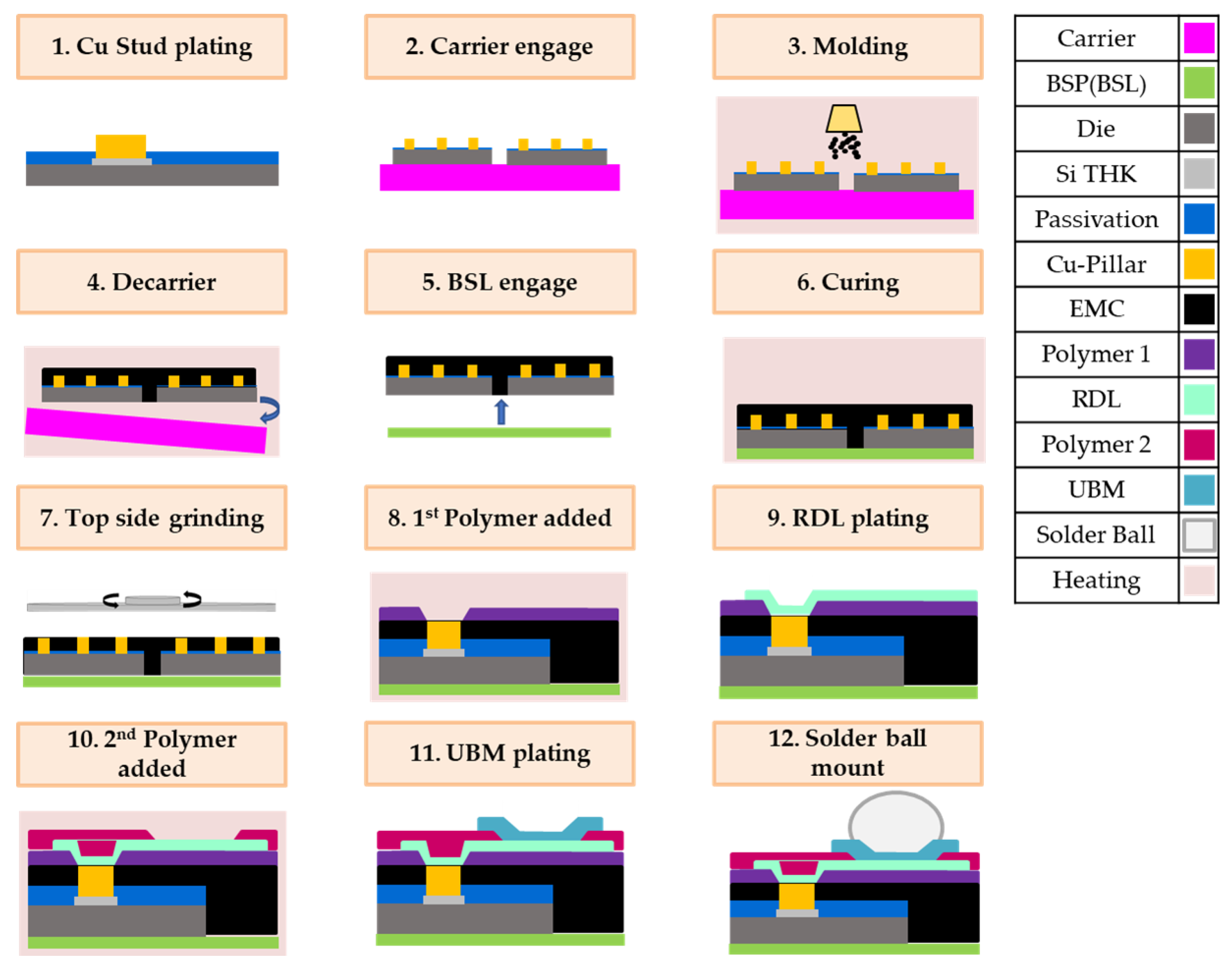
2.1. Structure Establishment
2.2. Boundary Condition Settings
2.3. Establishing Material Parameters
3. Results
4. Discussion
4.1. Effect of Material Properties on Warpage
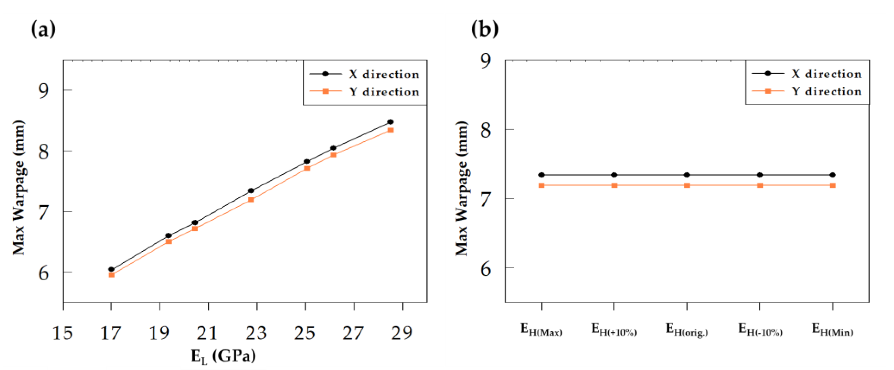
4.1.1. Effect of Young’s Modulus
4.1.2. Effect of CTE
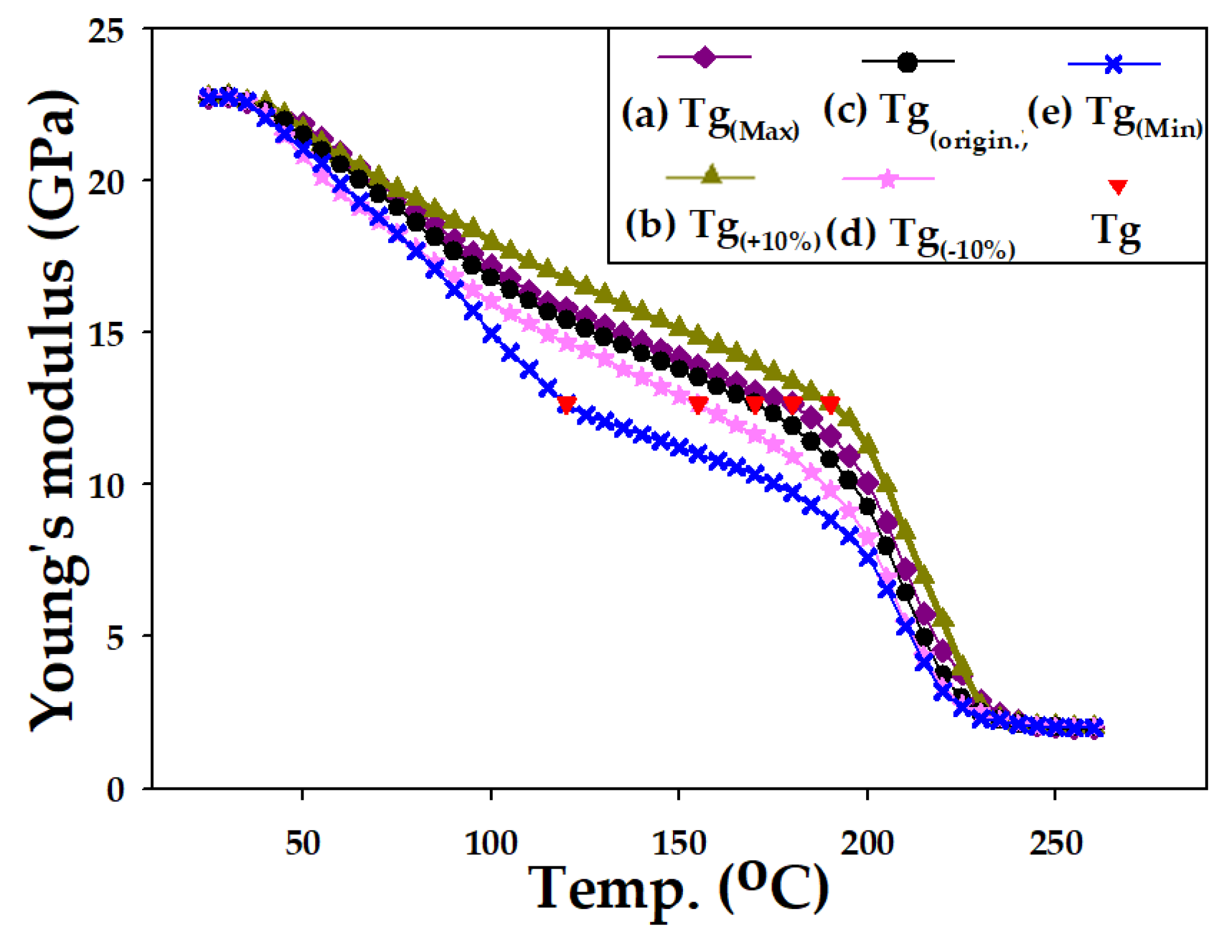
4.1.3. Effect of Tg
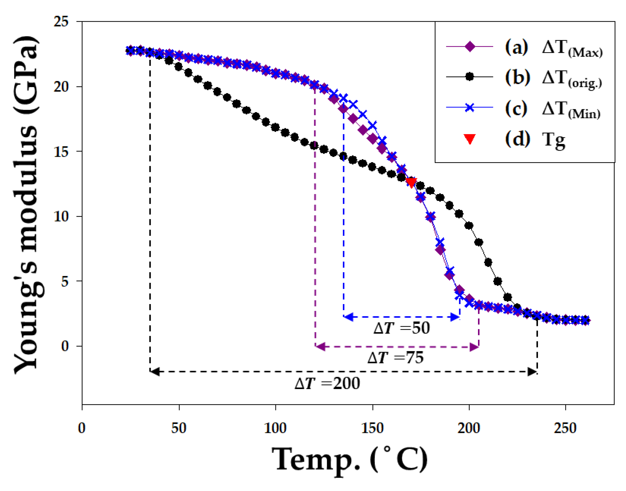
4.1.4. Effect of ∆T
4.2. Optimization Design of EMC Material Properties
5. Conclusions
Author Contributions
Funding
Institutional Review Board Statement
Informed Consent Statement
Data Availability Statement
Acknowledgments
Conflicts of Interest
References
- Hou, F.Z.; Lin, T.Y.; Cao, L.Q.; Liu, F.M.; Li, J.; Fan, X.J.; Zhang, G.Q. Experimental Verification and Optimization Analysis of Warpage for Panel-Level Fan-Out Package. IEEE Trans. Compon. Packag. Manuf. Technol. 2017, 7, 1721–1728. [Google Scholar] [CrossRef]
- Lau, J.H.; Li, M.; Yang, L.; Li, M.; Xu, I.; Chen, T.; Chen, S.; Yong, Q.X.; Madhukumar, J.P.; Kai, W.; et al. Warpage Measurements and Characterizations of Fan-Out Wafer-Level Packaging With Large Chips and Multiple Redistributed Layers. IEEE Trans. Compon. Packag. Manuf. Technol. 2018, 8, 1729–1737. [Google Scholar] [CrossRef]
- Su, M.; Cao, L.; Lin, T.; Chen, F.; Li, J.; Chen, C.; Tian, G. Warpage simulation and experimental verification for 320 mm × 320 mm panel level fan-out packaging based on die-first process. Microelectron. Reliab. 2018, 83, 29–38. [Google Scholar] [CrossRef]
- Chiu, T.C.; Yeh, E.Y. Warpage simulation for the reconstituted wafer used in fan-out wafer level packaging. Microelectron. Reliab. 2018, 80, 14–23. [Google Scholar] [CrossRef]
- Yang, G.N.; Kuang, Z.L.; Lai, H.Q.; Liu, Y.; Cui, R.B.; Cao, J.; Zhang, Y.; Cui, C.Q. A Quantitative Model to Understand the Effect of Gravity on the Warpage of Fan-Out Panel-Level Packaging. IEEE Trans. Compon. Packag. Manuf. Technol. 2021, 11, 2022–2030. [Google Scholar] [CrossRef]
- Chen, C.; Su, M.Y.; Ma, R.; Zhou, Y.Y.; Li, J.; Cao, L.Q. Investigation of Warpage for Multi-Die Fan-Out Wafer-Level Packaging Process. Materials 2022, 15, 1683. [Google Scholar] [CrossRef] [PubMed]
- Che, F.X.; Ho, D.; Chai, T.C. Study on Warpage and Reliability of Fan-Out Interposer Technology. IEEE Trans. Compon. Packag. Manuf. Technol. 2019, 9, 786–796. [Google Scholar] [CrossRef]
- Cheng, H.C.; Wu, Z.D.; Liu, Y.C. Viscoelastic Warpage Modeling of Fan-Out Wafer-Level Packaging During Wafer-Level Mold Cure Process. IEEE Trans. Compon. Packag. Manuf. Technol. 2020, 10, 1240–1250. [Google Scholar] [CrossRef]
- Chen, C.; Yu, D.Q.; Wang, T.; Xiao, Z.Y.; Wan, L.X. Warpage Prediction and Optimization for Embedded Silicon Fan-Out Wafer-Level Packaging Based on an Extended Theoretical Model. IEEE Trans. Compon. Packag. Manuf. Technol. 2019, 9, 845–853. [Google Scholar] [CrossRef]
- Hamaguchi, K.; Noma, H.; Takahashi, H.; Suzuki, N.; Nonaka, T. Warpage Study of FO-WLP Build Up by Material Properties and Process. In Proceedings of the 2016 6th Electronic System-Integration Technology Conference (ESTC), Grenoble, France, 13–15 September 2016; pp. 1–4. [Google Scholar]
- Marius, V.D.; Saskia, H.; Andreas, S.; Hans, W.; Olaf, W.; Martin, S.R. Experimental and simulative study of warpage behavior for fan-out wafer-level packaging. Microelectron. Reliab. 2022, 135, 114585. [Google Scholar]
- Lee, C.C.; Lee, C.C.; Chang, C.P. Simulation methodology development of warpage estimation for epoxy molding compound under considerations of stress relaxation characteristics and curing conditions applied in semiconductor packaging. Mater. Sci. Semicond. Process. 2022, 145, 106637. [Google Scholar] [CrossRef]
- Wang, S.H.; Hsu, W.; Liou, Y.Y.; Huang, P.C.; Lee, C.C. Reliability Assessment of Thermocompressed Epoxy Molding Compound through Glass via Interposer Architecture by the Submodeling Simulation Approach. Materials 2022, 15, 7357. [Google Scholar] [CrossRef] [PubMed]
- Chen, H.L.; Chiang, K.N. The Effect of Geometric and Material Uncertainty on Debonding Warpage in Fan-Out Panel Level Packaging. In Proceedings of the 2023 24th International Conference on Thermal, Mechanical and Multi-Physics Simulation and Experiments in Microelectronics and Microsystems (EuroSimE), Graz, Austria, 16–19 April 2023; pp. 1–6. [Google Scholar]
- Shih, M.K.; Huang, C.Y.; Chen, T.H.; Wang, C.C.; Tarng, D.; Hung, C.P. Electrical, Thermal, and Mechanical Characterization of eWLB, Fully Molded Fan-Out Package, and Fan-Out Chip Last Package. IEEE Trans. Compon. Packag. Manuf. Technol. 2019, 9, 1765–1775. [Google Scholar] [CrossRef]
- Wu, M.L.; Lan, J.S. Simulation and Experimental Study of the Warpage of Fan-Out Wafer-Level Packaging: The Effect of the Manufacturing Process and Optimal Design. IEEE Trans. Compon. Packag. Manuf. Technol. 2019, 9, 1396–1405. [Google Scholar] [CrossRef]


| Items | E(EL, EH) | CTE(α1, α2) | Tg | ∆T | Quantified Analysis of Wafer Warpage | Optimization of EMC |
|---|---|---|---|---|---|---|
| [1] | X | α: O | X | X | CTE: O | X |
| [2] | X | X | X | X | X | X |
| [3] | X | α: O | X | X | CTE: O | X |
| [4] | X | X | X | X | X | X |
| [5] | X | X | X | X | X | X |
| [6] | X | α: O | X | X | CTE: O | X |
| [7] | E: O | α: O | X | X | E, CTE: O | X |
| [8] | E: O | α: O | X | X | E, CTE: O | X |
| [9] | E: O | α: O | X | X | E, CTE: O | X |
| [10] | E: O | α: O | O | X | E, CTE, Tg: O | O (warpage: 65%↓) |
| [11] | X | X | X | X | X | X |
| [12] | X | X | X | X | X | X |
| [13] | X | X | X | X | X | X |
| [14] | X | X | X | X | X | X |
| This work | EL: O, EH: O | α1: O, α2: O | O | O | (EL, EH), (α1, α2), Tg, ∆T: O | O (warpage: 92.58%↓ (X-direction) and 93.74%↓ (Y-direction)) |
| Information | Value |
|---|---|
| Wafer size (mm2) | 150 × 150 × π |
| Package size (mm2) | 5.46 × 4.49 |
| Molding compound thickness (µm) | 625 |
| Die size (mm2) | 5.25 × 4.28 |
| Die thickness (µm) | 500 |
| Passivation thickness (µm) | 6 |
| Cu-pillar pitch (µm) | 120 |
| Cu Pillar (Cu) | Die (Si 100) | Passivation | EMC | |
|---|---|---|---|---|
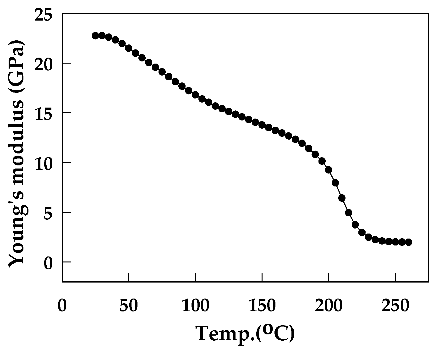
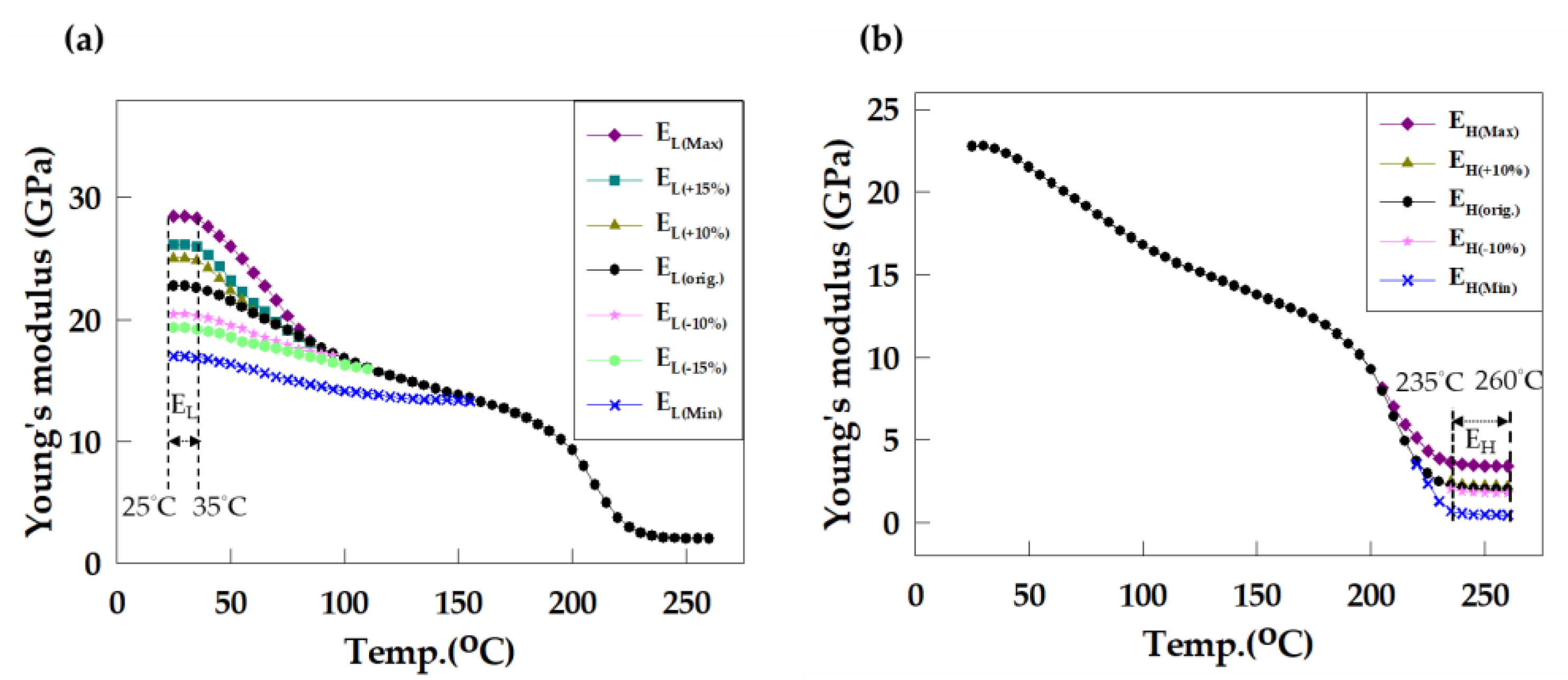
| Young’s modulus (Gpa) | 120 | 131 | 66 | Figure 6 |
| Poisson’s ratio | 0.34 | 0.27 | 0.17 | 0.3 |
| Density (kg/m3) | 8960 | 2330 | 2270 | 2040 |
| CTE (ppm/°C) | 16.5 | 2.8 | 0.56 | α1: 8/α2: 25 |
| Parameter | Value |
|---|---|
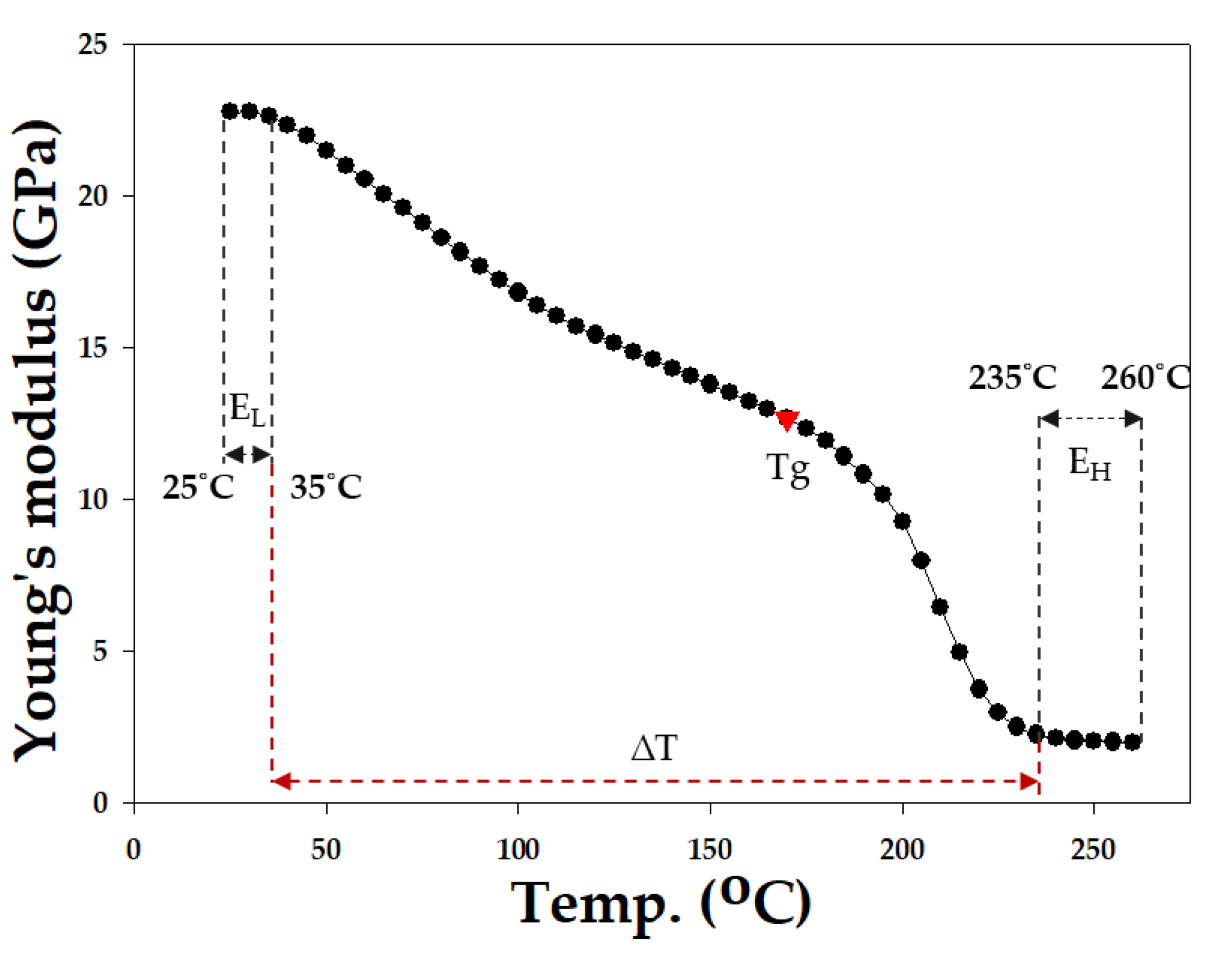
| Young’s modulus (Gpa) | EL: 8.96~28.5/EH: 0.45~3.4 |
| Tg (°C) | 120~180 |
| ∆T (°C) | 50~75 |
| CTE (ppm/°C) | α1:0.32~16/α2:22~56 |
| Process Step | Max Wafer Warpage (mm) | ||
|---|---|---|---|
| Experimental Value | Simulation Value | Error (%) | |
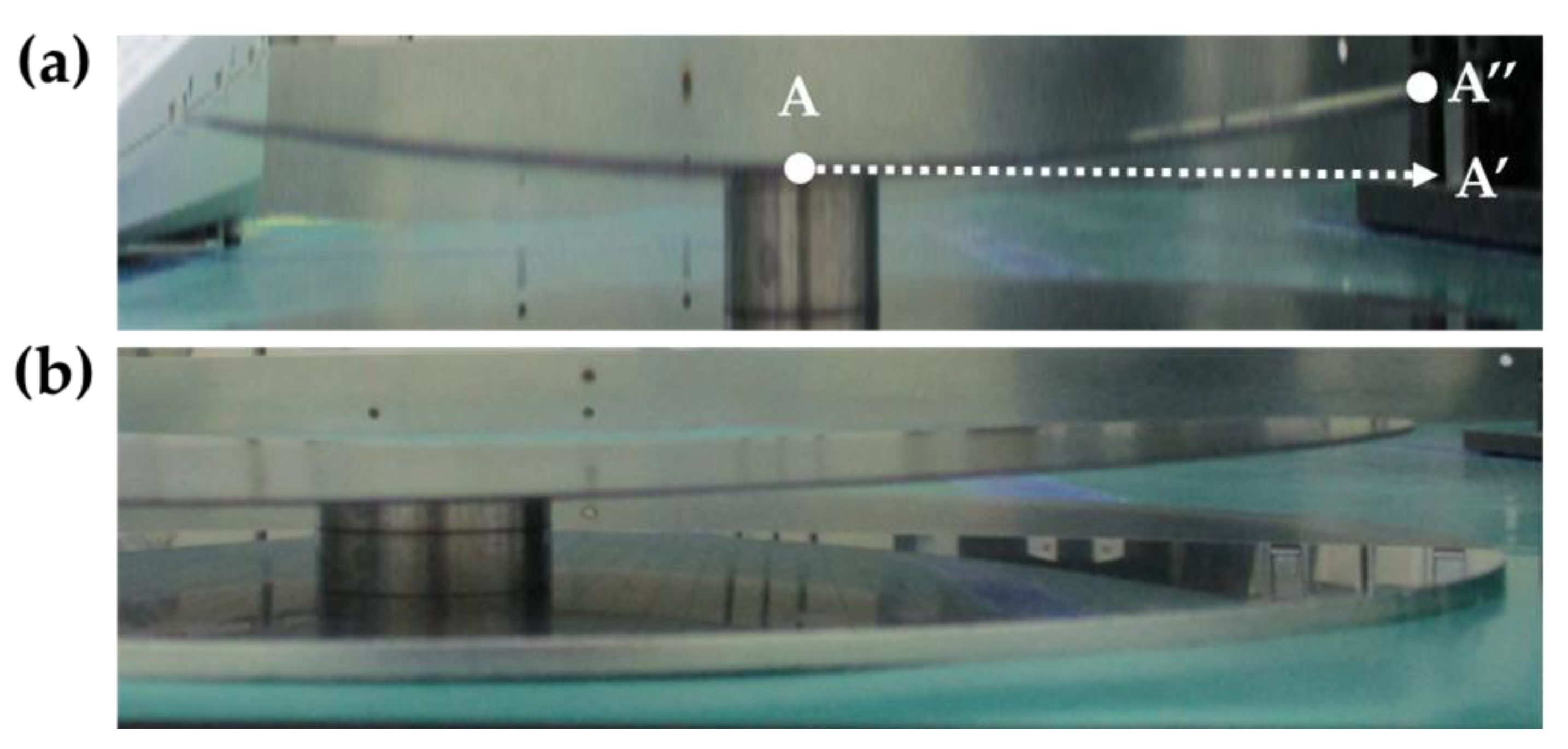
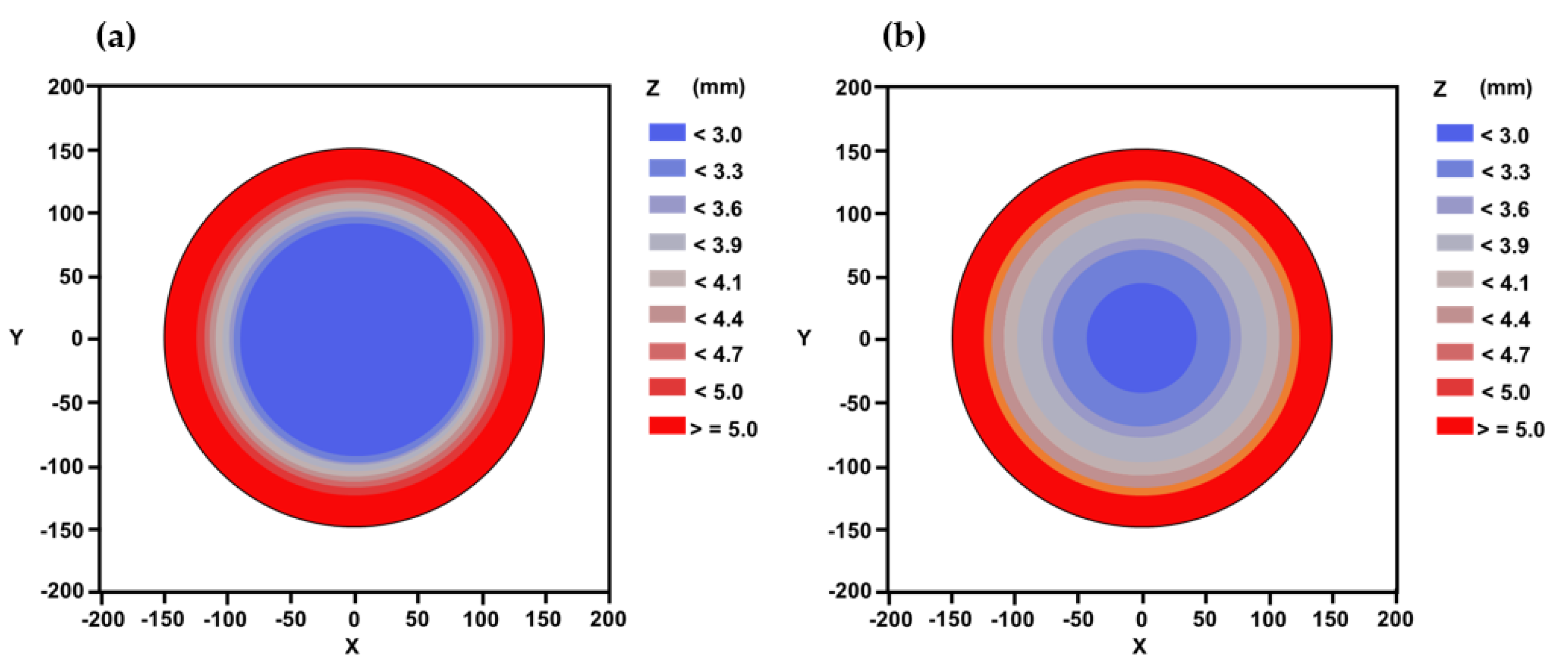
| 4. Decarrier | 7.329 ± 0.3 (concave) | X axis: 7.34 Y axis: 7.189 | 0.15 |
| ModulatedEL | Average EL (Gpa) | Max Warpage (mm) | Variation (%) | ||
| X Direction | Y Direction | X Direction | Y Direction | ||
| EL(+25%(Max)) | 28.50 | 8.477 | 8.342 | +15.50% | +16.03% |
| EL(+15%) | 26.15 | 8.046 | 7.931 | +9.62% | +10.32% |
| EL(+10%) | 25.05 | 7.825 | 7.71 | +6.61% | +7.25% |
| EL(orig.) | 22.75 | 7.34 | 7.189 | 0% | 0% |
| EL(−10%) | 20.45 | 6.81 | 6.717 | −7.22% | −6.57% |
| EL(−15%) | 19.35 | 6.595 | 6.504 | −10.15% | −9.53% |
| EL(−25%(Min)) | 17.00 | 6.038 | 5.953 | −17.74% | −17.19% |
| Modulated EH | Average EH (Gpa) | Max Warpage (mm) | Variation (%) | ||
| X Direction | Y Direction | X Direction | Y Direction | ||
| EH(Max) | 3.40 | 7.34 | 7.189 | 0% | 0% |
| EH(+10%) | 2.19 | 7.34 | 7.189 | 0% | 0% |
| EH(orig.) | 1.99 | 7.34 | 7.189 | 0% | 0% |
| EH(−10%) | 1.79 | 7.34 | 7.189 | 0% | 0% |
| EH(Min) | 0.45 | 7.34 | 7.189 | 0% | 0% |
| Modulated α1 | CTE Value (ppm/°C) | Max Warpage (mm) | Variation (%) | ||
| X Direction | Y Direction | X Direction | Y Direction | ||
| α1(+90%(Max)) | α1: 15.5/α2: 25 | 13.839 | 13.804 | +88.54% | +92.01% |
| α1(+75%) | α1: 14/α2: 25 | 12.538 | 12.532 | +70.82% | +74.32% |
| α1(+50%) | α1: 12/α2: 25 | 10.813 | 10.734 | +47.32% | +49.31% |
| α1(+25%) | α1: 10/α2: 25 | 9.058 | 8.962 | +23.41% | +24.66% |
| α1(+15%) | α1: 9.2/α2: 25 | 8.337 | 8.266 | +13.58% | +14.98% |
| α1(+10%) | α1: 9/α2: 25 | 8.223 | 8.082 | +12.03% | +12.42% |
| α1(orig.) | α1: 8/α2: 25 | 7.34 | 7.189 | 0% | 0% |
| α1(−10%) | α1: 7/α2: 25 | 6.431 | 6.317 | −12.38% | −12.13% |
| α1(−15%) | α1: 6.8/α2: 25 | 6.272 | 6.133 | −14.55% | −14.69% |
| α1(−25%) | α1: 6/α2: 25 | 5.516 | 5.462 | −24.85% | −24.02% |
| α1(−50%) | α1: 4/α2: 25 | 3.753 | 3.665 | −48.87% | −49.02% |
| α1(−75%) | α1: 2/α2: 25 | 1.984 | 1.886 | −72.97% | −73.77% |
| α1(−90%(Min)) | α1: 0.5/α2: 25 | 0.64 | 0.554 | −91.28% | −92.29% |
| Modulated α2 | CTE Value(ppm/°C) | Max Warpage (mm) | Variation (%) | ||
| X Direction | Y Direction | X Direction | Y Direction | ||
| α2(Max) | α1: 8/α2: 55 | 7.278 | 7.223 | −0.85% | +0.47% |
| α2(+10%) | α1: 8/α2: 27 | 7.365 | 7.175 | +0.34% | −0.20% |
| α2(orig.) | α1: 8/α2: 25 | 7.34 | 7.189 | 0% | 0% |
| α2(−10%) | α1: 8/α2: 23 | 7.329 | 7.256 | −0.15% | +0.93% |
| α2(Min) | α1: 8/α2: 22 | 7.318 | 7.212 | −0.30% | +0.32% |
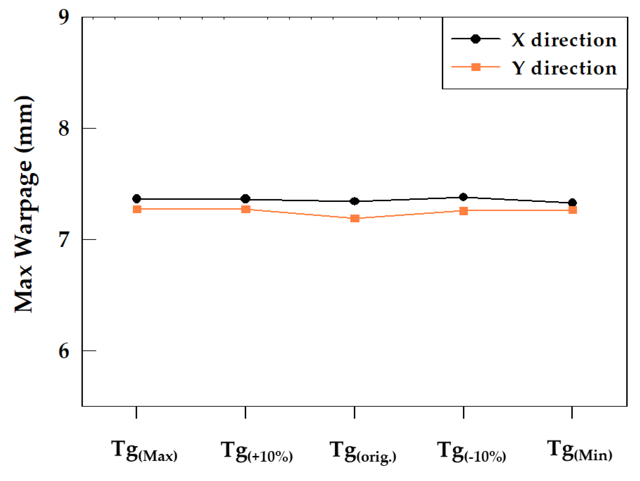
| Parameter | Tg(Max) | Tg(+10%) | Tg(orig.) | Tg(−10%) | Tg(Min) |
|---|---|---|---|---|---|
| Young’s modulus (Gpa) | Figure 12-(a) | Figure 12-(b) | Figure 12-(c) | Figure 12-(d) | Figure 12-(e) |
| Tg (°C) | 180 | 187 | 170 | 153 | 120 |
| CTE (ppm/°C) | α1: 8/α2: 25 | α1: 8/α2: 25 | α1: 8/α2: 25 | α1: 8/α2: 25 | α1: 8/α2: 25 |
| Maximum Warpage in X direction (mm) | 7.361 | 7.361 | 7.34 | 7.376 | 7.324 |
| Maximum Warpage in Y direction (mm) | 7.271 | 7.269 | 7.189 | 7.255 | 7.264 |
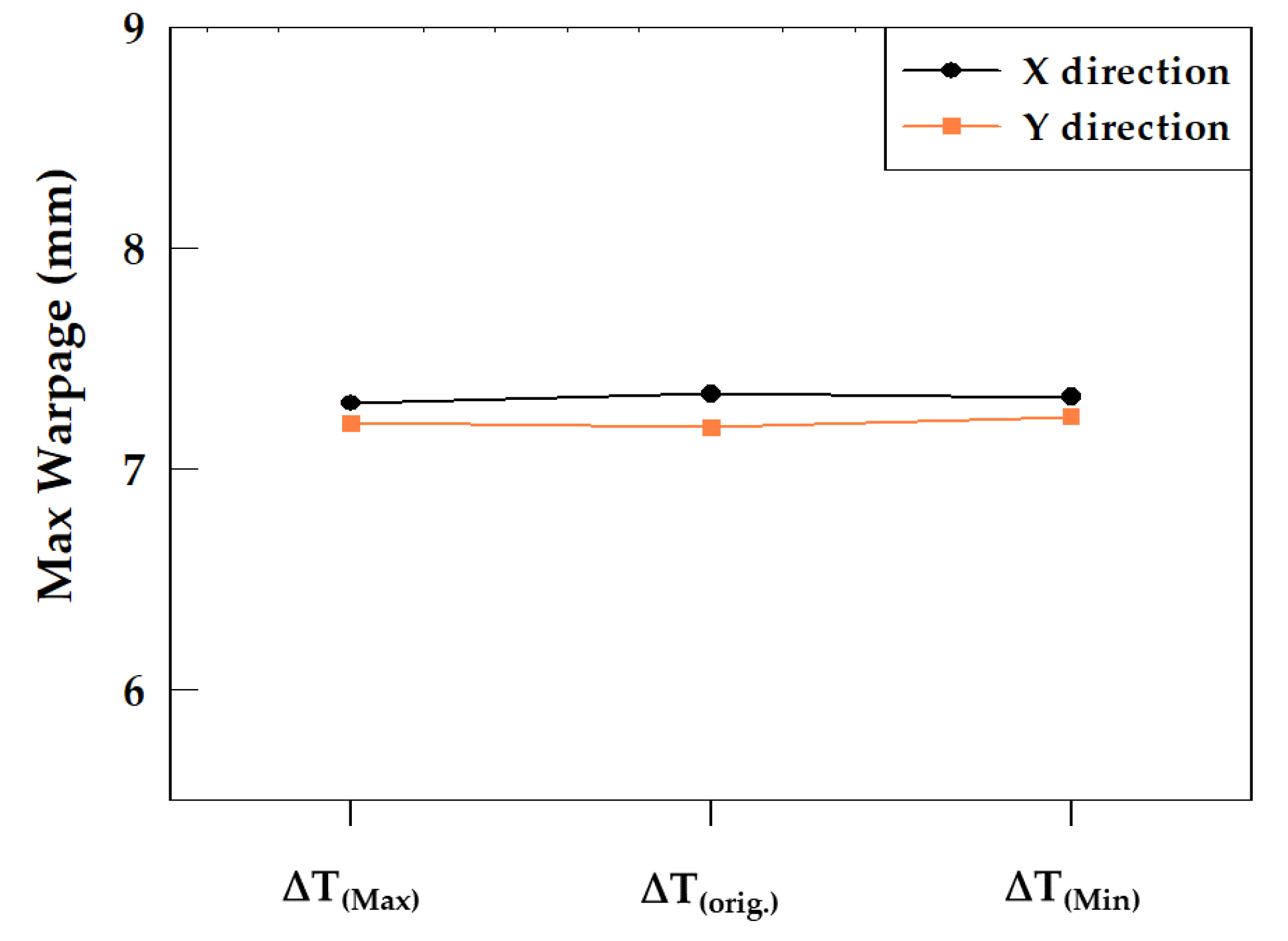
| Parameter | ∆T(Max) | ∆T(orig.) | ∆T(Min) |
|---|---|---|---|
| Young’s modulus (GPa) | Figure 14-(a) | Figure 14-(b) | Figure 14-(c) |
| Tg (°C) | 170 | 170 | 170 |
| ∆T (°C) | 75 | 200 | 50 |
| CTE (ppm/°C) | α1: 8/α2: 25 | α1: 8/α2: 25 | α1: 8/α2: 25 |
| Maximum Warpage in X direction (mm) | 7.299 | 7.34 | 7.326 |
| Maximum Warpage in Y direction (mm) | 7.208 | 7.189 | 7.238 |
| No. | Modulated EL & α1 | Max Warpage (mm) | Variation (%) | ||
|---|---|---|---|---|---|
| X Direction | Y Direction | X Direction | Y Direction | ||
| 1 | EL(orig.)α1(orig.) | 7.34 | 7.189 | 0% | 0% |
| 2 | EL(+25%(Max))α1(+90%(Max)) | 16.302 | 16.13 | +122.10% | +124.37% |
| 3 | EL(−10%)α1(+10%) | 7.644 | 7.524 | +4.14% | +4.66% |
| 4 | EL(+10%)α1(−10%) | 6.876 | 6.758 | −6.32% | −6.00% |
| 5 | EL(−10%)α1(−10%) | 6.05 | 5.963 | −17.58% | −17.05% |
| 6 | EL(+25%(Max))α1(orig.) | 8.477 | 8.342 | +15.50% | +16.03% |
| 7 | EL(+25%(Max))α1(−10%) | 7.449 | 7.263 | +1.49% | +1.03% |
| 8 | EL(+25%(Max))α1(−15%) | 7.238 | 7.08 | −1.39% | −1.52% |
| 9 | EL(Max)α1(−90%(Min)) | 0.545 | 0.45 | −92.58% | −93.74% |
| 10 | EL(+15%)α1(−90%(Min)) | 0.588 | 0.495 | −91.99% | −93.11% |
| 11 | EL+10%)α1(−90%(Min)) | 0.608 | 0.514 | −91.72% | −92.85% |
| 12 | EL(−10%)α1(−90%(Min)) | 0.678 | 0.59 | −90.76% | −91.79% |
| 13 | EL(−15%)α1(−90%(Min)) | 0.692 | 0.606 | −90.57% | −91.57% |
| 14 | EL(−25%(Min))α1(−90%(Min)) | 0.719 | 0.634 | −90.2% | −91.2% |
Disclaimer/Publisher’s Note: The statements, opinions and data contained in all publications are solely those of the individual author(s) and contributor(s) and not of MDPI and/or the editor(s). MDPI and/or the editor(s) disclaim responsibility for any injury to people or property resulting from any ideas, methods, instructions or products referred to in the content. |
© 2023 by the authors. Licensee MDPI, Basel, Switzerland. This article is an open access article distributed under the terms and conditions of the Creative Commons Attribution (CC BY) license (https://creativecommons.org/licenses/by/4.0/).
Share and Cite
Chuang, W.-C.; Huang, Y.; Chen, P.-E. Exploring the Influence of Material Properties of Epoxy Molding Compound on Wafer Warpage in Fan-Out Wafer-Level Packaging. Materials 2023, 16, 3482. https://doi.org/10.3390/ma16093482
Chuang W-C, Huang Y, Chen P-E. Exploring the Influence of Material Properties of Epoxy Molding Compound on Wafer Warpage in Fan-Out Wafer-Level Packaging. Materials. 2023; 16(9):3482. https://doi.org/10.3390/ma16093482
Chicago/Turabian StyleChuang, Wan-Chun, Yi Huang, and Po-En Chen. 2023. "Exploring the Influence of Material Properties of Epoxy Molding Compound on Wafer Warpage in Fan-Out Wafer-Level Packaging" Materials 16, no. 9: 3482. https://doi.org/10.3390/ma16093482
APA StyleChuang, W.-C., Huang, Y., & Chen, P.-E. (2023). Exploring the Influence of Material Properties of Epoxy Molding Compound on Wafer Warpage in Fan-Out Wafer-Level Packaging. Materials, 16(9), 3482. https://doi.org/10.3390/ma16093482