

Selective-Area Growth Mechanism of GaN Microrods on a Plateau Patterned Substrate

 and
and
Abstract
1. Introduction
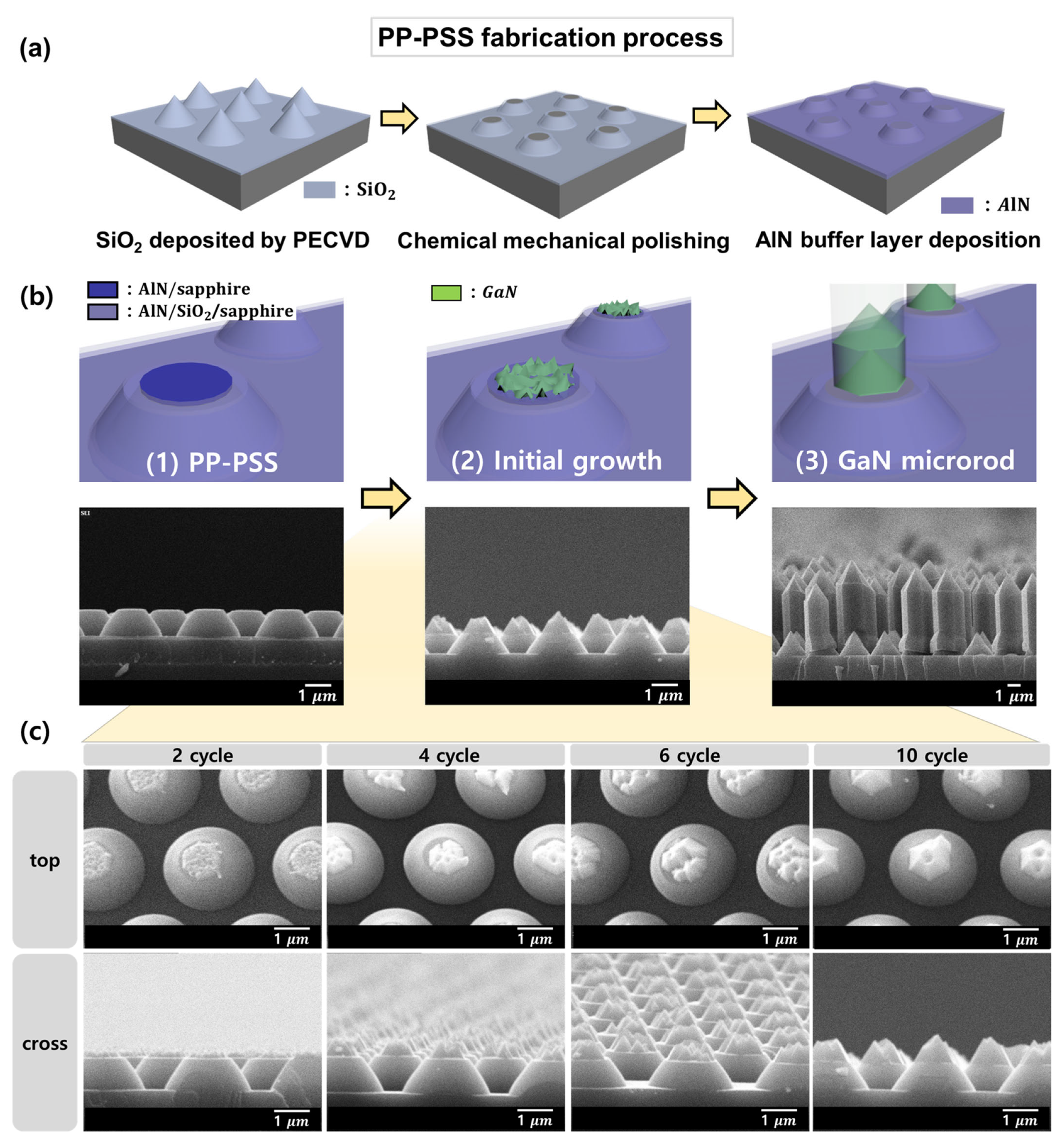
2. Materials and Methods
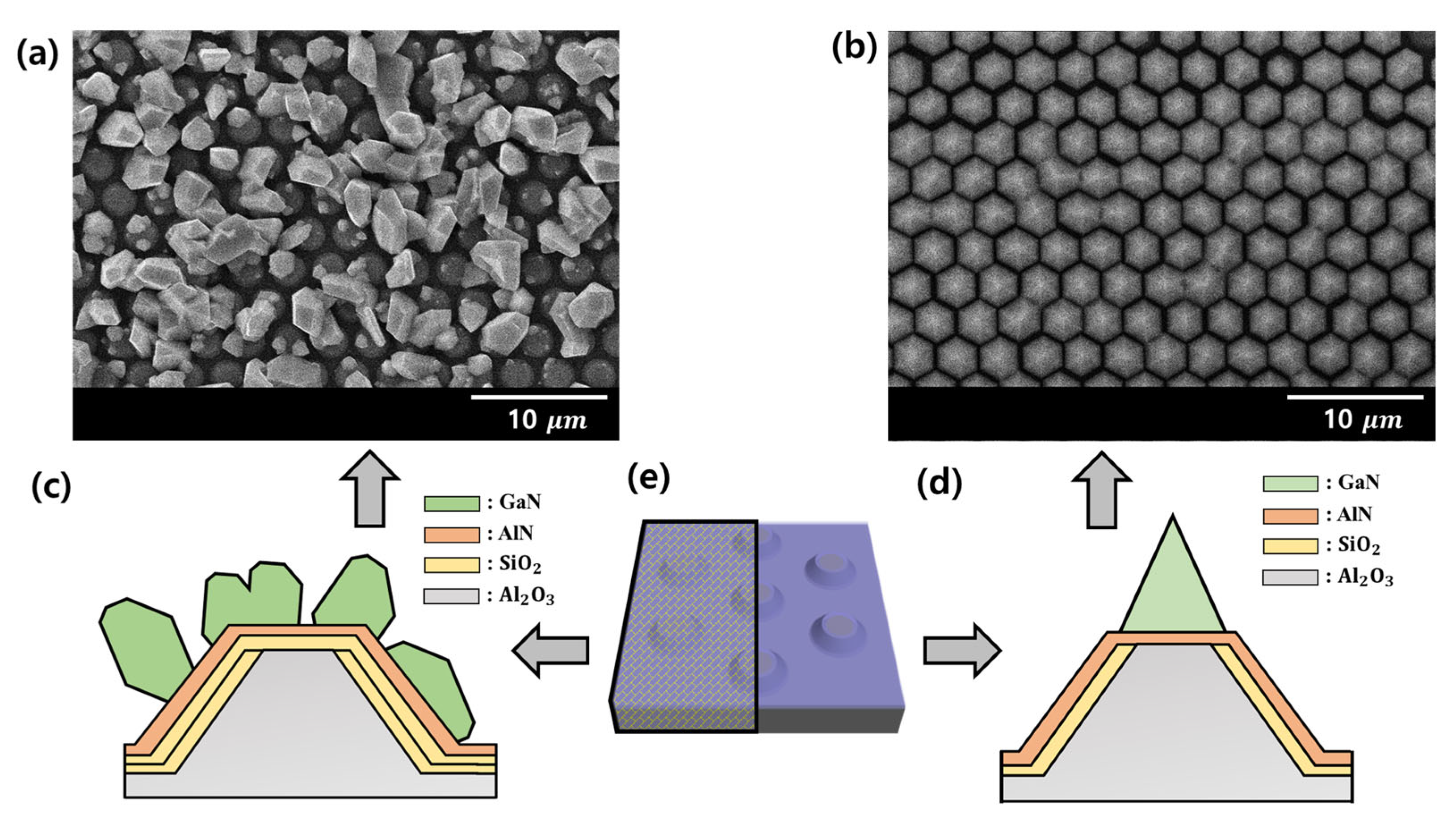
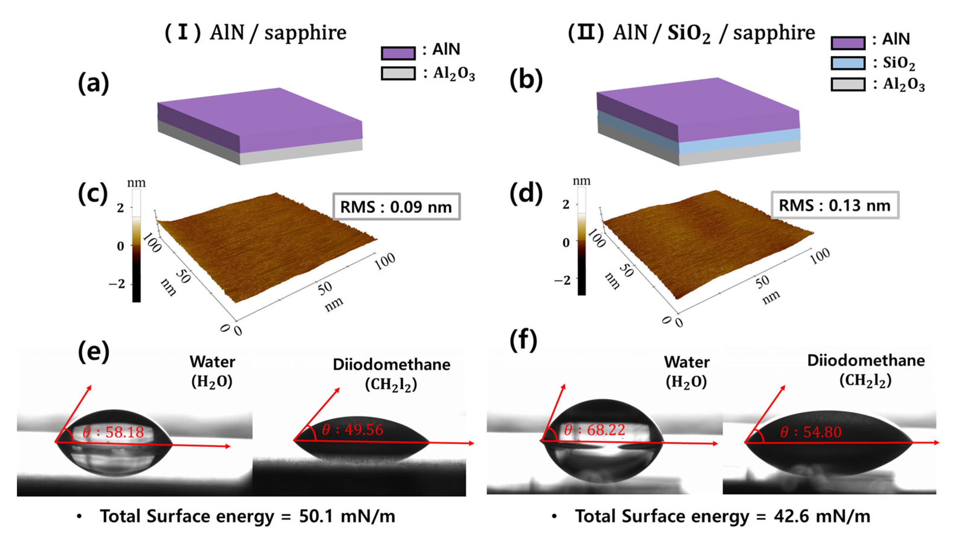
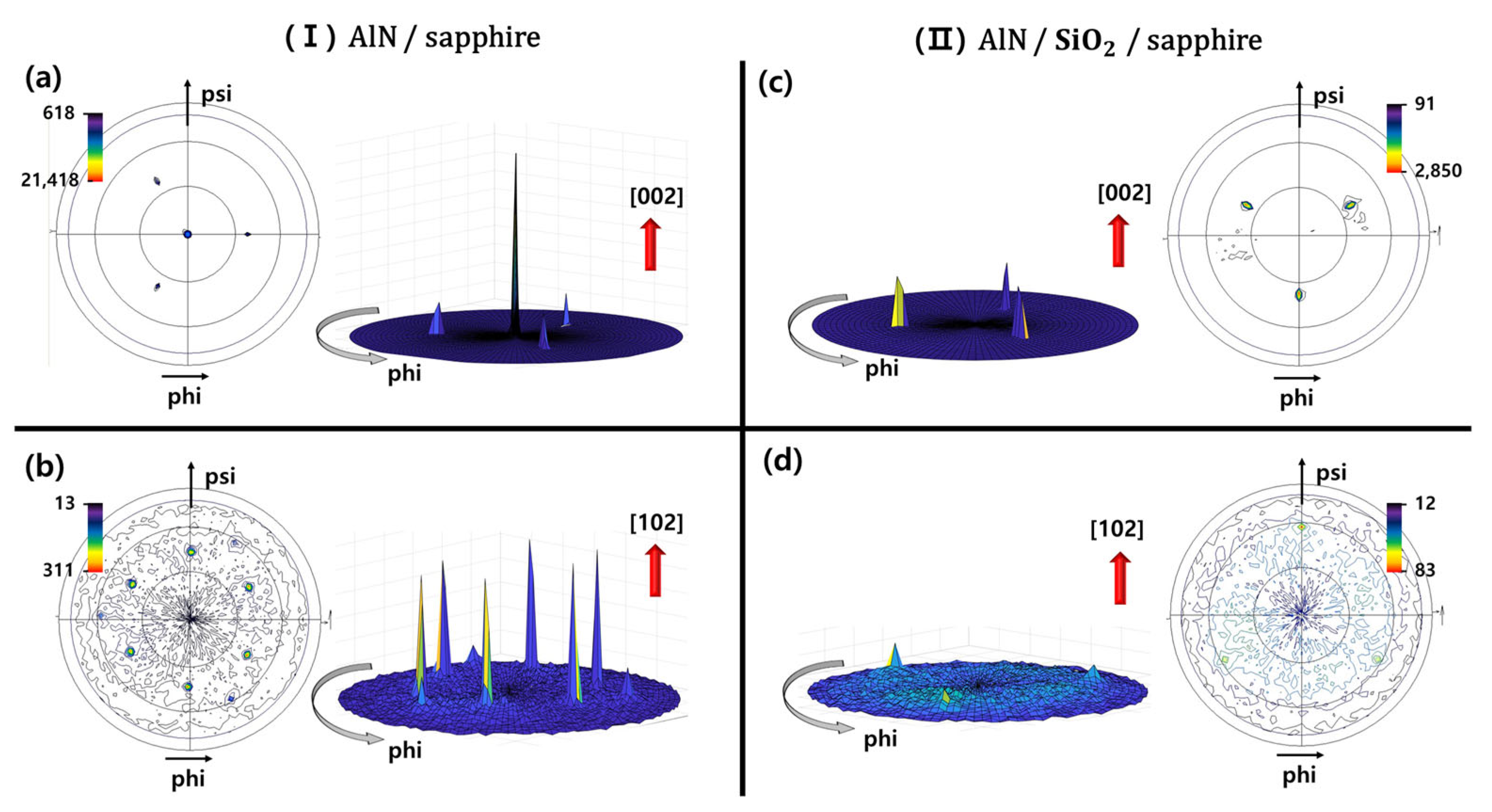
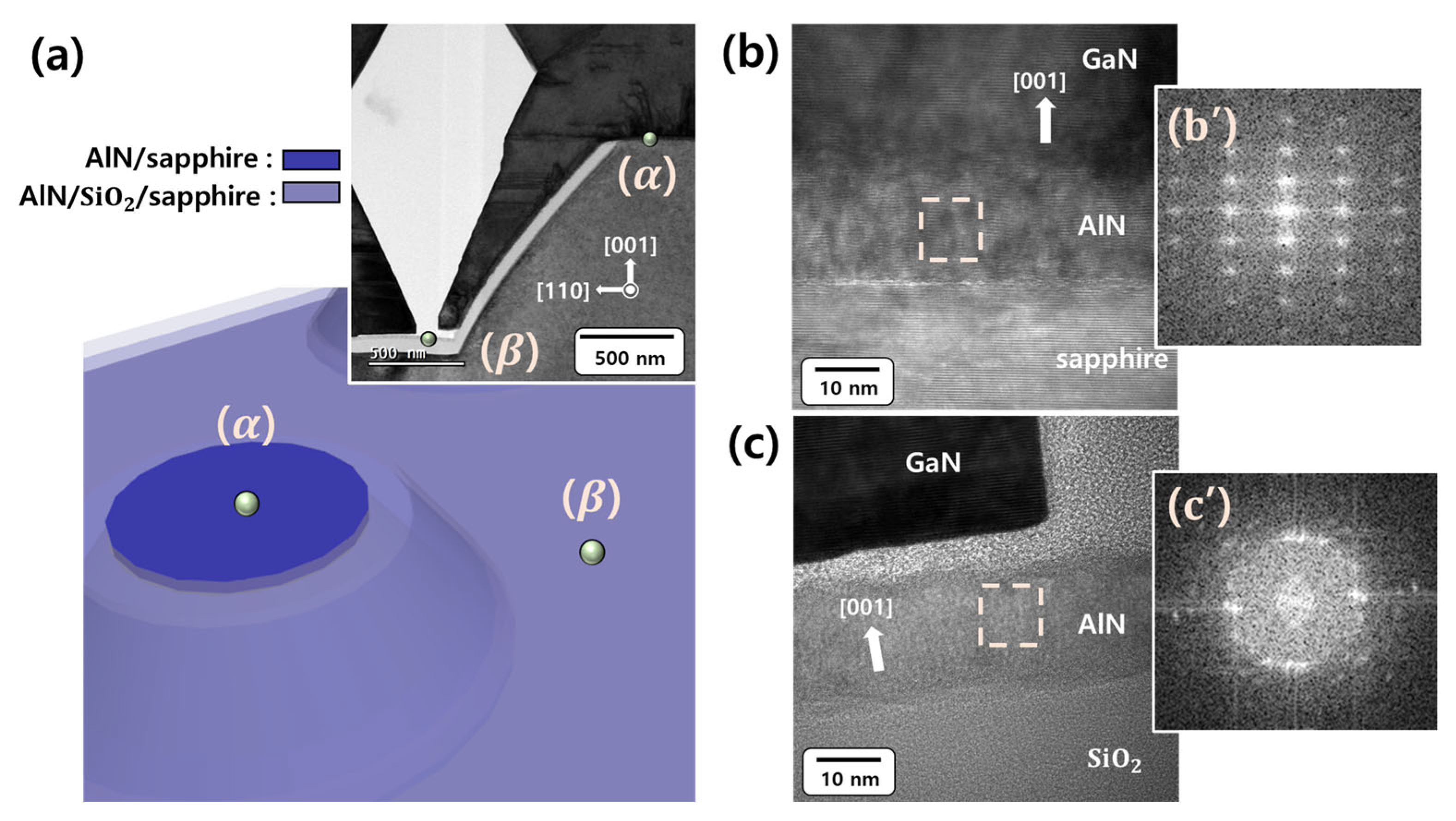
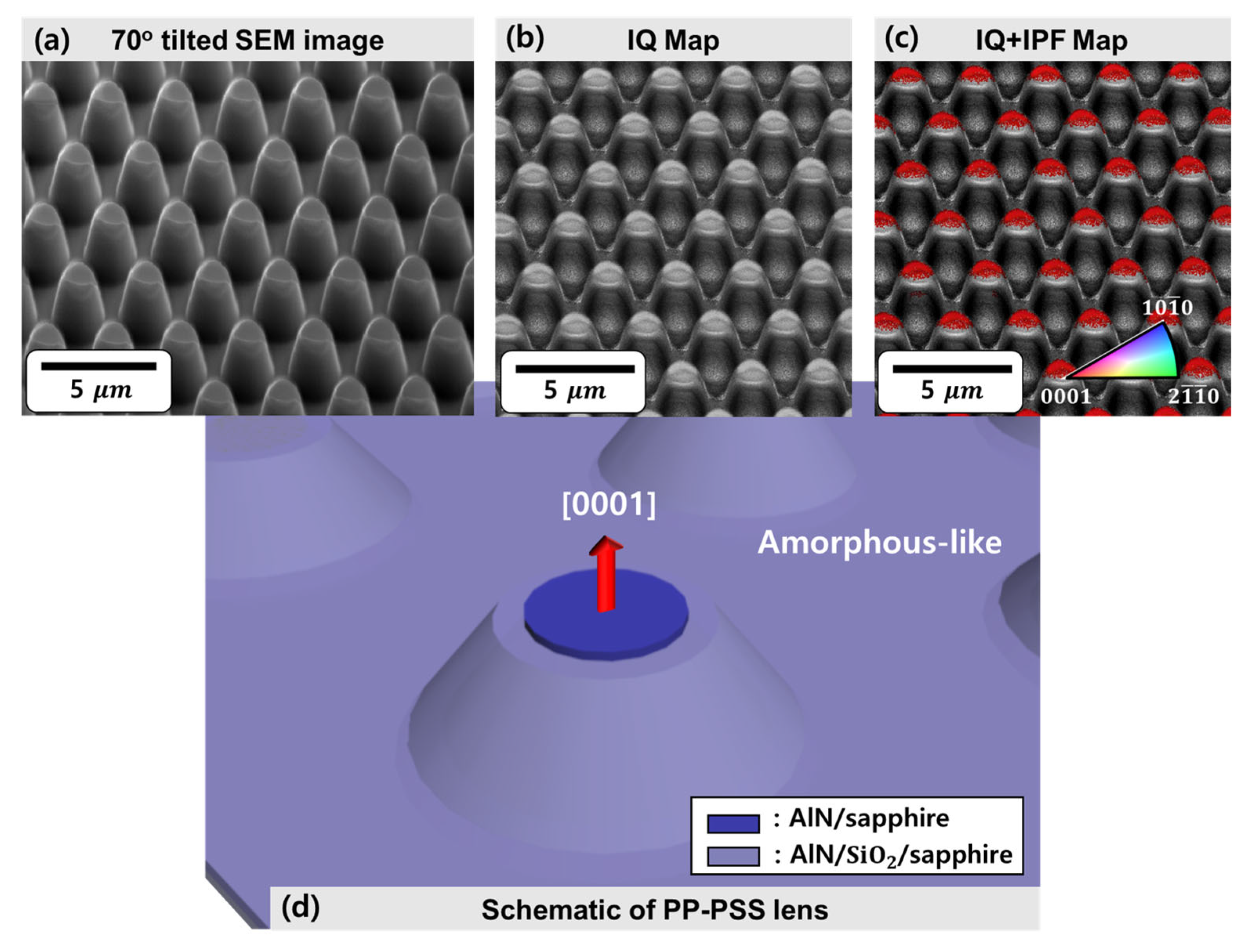
3. Results and Discussion
4. Conclusions
Author Contributions
Funding
Institutional Review Board Statement
Informed Consent Statement
Data Availability Statement
Conflicts of Interest
References
- Ra, Y.-H.; Wang, R.; Woo, S.Y.; Djavid, M.; Sadaf, S.M.; Lee, J.; Botton, G.A.; Mi, Z. Full-Color Single Nanowire Pixels for Projection Displays. Nano Lett. 2016, 16, 4608–4615. [Google Scholar] [CrossRef]
- Roccaforte, F.; Greco, G.; Fiorenza, P.; Iucolano, F. An Overview of Normally-Off GaN-Based High Electron Mobility Transistors. Materials 2019, 12, 1599. [Google Scholar] [CrossRef] [PubMed]
- Takeuchi, T.; Sota, S.; Katsuragawa, M.; Komori, M.; Takeuchi, H.; Amano, H.; Akasaki, I. Quantum-Confined Stark Effect due to Piezoelectric Fields in GaInN Strained Quantum Wells. Jpn. J. Appl. Phys. 1997, 36, L382–L385. [Google Scholar] [CrossRef]
- Huang, C.-F.; Tang, T.-Y.; Huang, J.-J.; Shiao, W.-Y.; Yang, C.C.; Hsu, C.-W.; Chen, L.C. Prestrained effect on the emission properties of InGaN∕GaN quantum-well structures. Appl. Phys. Lett. 2006, 89, 051913. [Google Scholar] [CrossRef]
- Lin, Y.-T.; Yeh, T.-W.; Daniel Dapkus, P. Mechanism of selective area growth of GaN nanorods by pulsed mode metalorganic chemical vapor deposition. Nanotechnology 2012, 23, 465601. [Google Scholar] [CrossRef]
- Colby, R.; Liang, Z.; Wildeson, I.H.; Ewoldt, D.A.; Sands, T.D.; García, R.E.; Stach, E.A. Dislocation Filtering in GaN Nanostructures. Nano Lett. 2010, 10, 1568–1573. [Google Scholar] [CrossRef]
- Bennett, S.E. Dislocations and their reduction in GaN. Mater. Sci. Technol. 2010, 26, 1017–1028. [Google Scholar] [CrossRef]
- Bougrioua, Z.; Gibart, P.; Calleja, E.; Jahn, U.; Trampert, A.; Ristic, J.; Utrera, M.; Nataf, G. Growth of freestanding GaN using pillar-epitaxial lateral overgrowth from GaN nanocolumns. J. Cryst. Growth 2007, 309, 113–120. [Google Scholar] [CrossRef]
- Liu, X.; Li, D.; Sun, X.; Li, Z.; Song, H.; Jiang, H.; Chen, Y. Stress-induced in situ epitaxial lateral overgrowth of high-quality GaN. CrystEngComm 2014, 16, 8058. [Google Scholar] [CrossRef]
- Miyamoto, Y.; Lu, W.; Sone, N.; Okuda, R.; Ito, K.; Okuno, K.; Mizutani, K.; Iida, K.; Ohya, M.; Iwaya, M.; et al. Crystal Growth and Characterization of n-GaN in a Multiple Quantum Shell Nanowire-Based Light Emitter with a Tunnel Junction. ACS Appl. Mater. Interfaces 2021, 13, 37883–37892. [Google Scholar] [CrossRef]
- Hong, Y.J.; Lee, C.-H.; Yoon, A.; Kim, M.; Seong, H.-K.; Chung, H.J.; Sone, C.; Park, Y.J.; Yi, G.-C. Visible-Color-Tunable Light-Emitting Diodes. Adv. Mater. 2011, 23, 3284–3288. [Google Scholar] [CrossRef]
- Bae, S.-Y.; Lee, J.-Y.; Min, J.-H.; Lee, D.-S. Morphology Evolution of Pulsed-Flux Ga-Polar GaN Nanorod Growth by Metal Organic Vapor Phase Epitaxy and Its Nucleation Dependence. Appl. Phys. Express 2013, 6, 075501. [Google Scholar] [CrossRef]
- Bae, S.-Y.; Lekhal, K.; Lee, H.-J.; Min, J.-W.; Lee, D.-S.; Honda, Y.; Amano, H. Selective-area growth of doped GaN nanorods by pulsed-mode MOCVD: Effect of Si and Mg dopants: Selective-area growth of doped GaN nanorods by pulsed-mode MOCVD. Phys. Status Solidi B 2017, 254, 1600722. [Google Scholar] [CrossRef]
- Sekiguchi, H.; Kishino, K.; Kikuchi, A. Emission color control from blue to red with nanocolumn diameter of InGaN/GaN nanocolumn arrays grown on same substrate. Appl. Phys. Lett. 2010, 96, 231104. [Google Scholar] [CrossRef]
- Liu, K.-W.; Young, S.-J.; Chang, S.-J.; Hsueh, T.-H.; Hung, H.; Chen, S.-X.; Chen, Y.-Z. Growth of gallium nitride on silicon by molecular beam epitaxy incorporating a chromium nitride interlayer. J. Alloys Compd. 2012, 511, 1–4. [Google Scholar] [CrossRef]
- Kishino, K.; Ishizawa, S. Selective-area growth of GaN nanocolumns on Si(111) substrates for application to nanocolumn emitters with systematic analysis of dislocation filtering effect of nanocolumns. Nanotechnology 2015, 26, 225602. [Google Scholar] [CrossRef]
- Tu, L.W.; Hsiao, C.L.; Chi, T.W.; Lo, I.; Hsieh, K.Y. Self-assembled vertical GaN nanorods grown by molecular-beam epitaxy. Appl. Phys. Lett. 2003, 82, 1601–1603. [Google Scholar] [CrossRef]
- Hersee, S.D.; Sun, X.; Wang, X. The Controlled Growth of GaN Nanowires. Nano Lett. 2006, 6, 1808–1811. [Google Scholar] [CrossRef]
- Roshko, A.; Brubaker, M.; Blanchard, P.; Harvey, T.; Bertness, K. Selective Area Growth and Structural Characterization of GaN Nanostructures on Si(111) Substrates. Crystals 2018, 8, 366. [Google Scholar] [CrossRef]
- Nami, M.; Eller, R.F.; Okur, S.; Rishinaramangalam, A.K.; Liu, S.; Brener, I.; Feezell, D.F. Tailoring the morphology and luminescence of GaN/InGaN core–shell nanowires using bottom-up selective-area epitaxy. Nanotechnology 2017, 28, 025202. [Google Scholar] [CrossRef]
- Kishino, K.; Sekiguchi, H.; Kikuchi, A. Improved Ti-mask selective-area growth (SAG) by rf-plasma-assisted molecular beam epitaxy demonstrating extremely uniform GaN nanocolumn arrays. J. Cryst. Growth 2009, 311, 2063–2068. [Google Scholar] [CrossRef]
- Albert, S.; Bengoechea-Encabo, A.; Sánchez-García, M.A.; Kong, X.; Trampert, A.; Calleja, E. Selective area growth of In(Ga)N/GaN nanocolumns by molecular beam epitaxy on GaN-buffered Si(111): From ultraviolet to infrared emission. Nanotechnology 2013, 24, 175303. [Google Scholar] [CrossRef]
- Bertness, K.A.; Sanders, A.W.; Rourke, D.M.; Harvey, T.E.; Roshko, A.; Schlager, J.B.; Sanford, N.A. Controlled Nucleation of GaN Nanowires Grown with Molecular Beam Epitaxy. Adv. Funct. Mater. 2010, 20, 2911–2915. [Google Scholar] [CrossRef]
- Kano, T.; Yoshida, J.; Miyagawa, R.; Mizuno, Y.; Oto, T.; Kishino, K. GaN nanocolumn arrays with diameter <30 nm prepared by two-step selective area growth. Electron. Lett. 2015, 51, 2125–2126. [Google Scholar] [CrossRef]
- Schumann, T.; Gotschke, T.; Limbach, F.; Stoica, T.; Calarco, R. Selective-area catalyst-free MBE growth of GaN nanowires using a patterned oxide layer. Nanotechnology 2011, 22, 095603. [Google Scholar] [CrossRef]
- Calleja, E.; Ristić, J.; Fernández-Garrido, S.; Cerutti, L.; Sánchez-García, M.A.; Grandal, J.; Trampert, A.; Jahn, U.; Sánchez, G.; Griol, A.; et al. Growth, morphology, and structural properties of group-III-nitride nanocolumns and nanodisks. Phys. Status Solidi B 2007, 244, 2816–2837. [Google Scholar] [CrossRef]
- Cheung, C.L.; Nikolić, R.J.; Reinhardt, C.E.; Wang, T.F. Fabrication of nanopillars by nanosphere lithography. Nanotechnology 2006, 17, 1339–1343. [Google Scholar] [CrossRef]
- Shin, S.W.; Lee, S.G.; Lee, J.; Whang, C.N.; Lee, J.-H.; Choi, I.-H.; Kim, T.G.; Song, J.H. Ion-beam nano-patterning by using porous anodic alumina as a mask. Nanotechnology 2005, 16, 1392–1395. [Google Scholar] [CrossRef]
- Contreras, A.M.; Grunes, J.; Yan, X.-M.; Liddle, A.; Somorjai, G.A. Fabrication of platinum nanoparticles and nanowires by electron beam lithography (EBL) and nanoimprint lithography (NIL): Comparison of ethylene hydrogenation kinetics. Catal. Lett. 2005, 100, 115–124. [Google Scholar] [CrossRef]
- Brubaker, M.D.; Duff, S.M.; Harvey, T.E.; Blanchard, P.T.; Roshko, A.; Sanders, A.W.; Sanford, N.A.; Bertness, K.A. Polarity-Controlled GaN/AlN Nucleation Layers for Selective-Area Growth of GaN Nanowire Arrays on Si(111) Substrates by Molecular Beam Epitaxy. Cryst. Growth Des. 2016, 16, 596–604. [Google Scholar] [CrossRef]
- Skjolding, L.H.D.; Spégel, C.; Emnéus, J.; Montelius, L. EBL/NIL fabrication and characterization of interdigitated electrodes for potential application in combinatorial studies. MRS Proc. 2007, 1024, 1024-A02-04. [Google Scholar] [CrossRef]
- Xu, H.; Kosma, V.; Giannelis, E.; Ober, C.K.; Sakai, K. EUV photolithography: Resist progress and challenges. In Proceedings of the Extreme Ultraviolet (EUV) Lithography IX; Felix, N.M., Goldberg, K.A., Eds.; SPIE: San Jose, CA, USA, 2018; p. 2. [Google Scholar]
- Xu, H.; Kosma, V.; Sakai, K.; Giannelis, E.P.; Ober, C.K. EUV photolithography: Resist progress in metal–organic complex photoresists. J. Micro/Nanolithogr. MEMS MOEMS 2018, 18, 1. [Google Scholar] [CrossRef]
- Gačević, Ž.; Gómez Sánchez, D.; Calleja, E. Formation Mechanisms of GaN Nanowires Grown by Selective Area Growth Homoepitaxy. Nano Lett. 2015, 15, 1117–1121. [Google Scholar] [CrossRef] [PubMed]
- Ahn, M.J.; Shim, K.; Jeong, W.S.; Kang, S.; Kim, H.; Kim, D.; Jhin, J.; Kim, J.; Byun, D. Deterministically-grown GaN microrods on a mask-free plateau patterned substrate. Vacuum 2023, 207, 111628. [Google Scholar] [CrossRef]
- Kozbial, A.; Li, Z.; Conaway, C.; McGinley, R.; Dhingra, S.; Vahdat, V.; Zhou, F.; D’Urso, B.; Liu, H.; Li, L. Study on the Surface Energy of Graphene by Contact Angle Measurements. Langmuir 2014, 30, 8598–8606. [Google Scholar] [CrossRef]
- Tsibouklis, J.; Nevell, T.G. Ultra-Low Surface Energy Polymers: The Molecular Design Requirements. Adv. Mater. 2003, 15, 647–650. [Google Scholar] [CrossRef]
- Park, S. Anti-adhesive layers on nickel stamps for nanoimprint lithography. Microelectron. Eng. 2004, 73–74, 196–201. [Google Scholar] [CrossRef]


| Contact Angle, [ , Average] | Surface Energy [mN/m] | |||||
|---|---|---|---|---|---|---|
| Sample | RMS (n ) | Water | Diiodo-methane | Disperse Component | Polar Component | Surface Energy |
| (I) AlN/sapphire | 0.09 | 58.2 | 49.5 | 34.5 | 15.5 | 50.1 |
| (II) AlN//sapphire | 0.13 | 68.2 | 54.8 | 31.6 | 11.0 | 42.6 |
Disclaimer/Publisher’s Note: The statements, opinions and data contained in all publications are solely those of the individual author(s) and contributor(s) and not of MDPI and/or the editor(s). MDPI and/or the editor(s) disclaim responsibility for any injury to people or property resulting from any ideas, methods, instructions or products referred to in the content. |
© 2023 by the authors. Licensee MDPI, Basel, Switzerland. This article is an open access article distributed under the terms and conditions of the Creative Commons Attribution (CC BY) license (https://creativecommons.org/licenses/by/4.0/).
Share and Cite
Ahn, M.-j.; Jeong, W.-s.; Shim, K.-y.; Kang, S.; Kim, H.; Kim, D.-s.; Jhin, J.; Kim, J.; Byun, D. Selective-Area Growth Mechanism of GaN Microrods on a Plateau Patterned Substrate. Materials 2023, 16, 2462. https://doi.org/10.3390/ma16062462
Ahn M-j, Jeong W-s, Shim K-y, Kang S, Kim H, Kim D-s, Jhin J, Kim J, Byun D. Selective-Area Growth Mechanism of GaN Microrods on a Plateau Patterned Substrate. Materials. 2023; 16(6):2462. https://doi.org/10.3390/ma16062462
Chicago/Turabian StyleAhn, Min-joo, Woo-seop Jeong, Kyu-yeon Shim, Seongho Kang, Hwayoung Kim, Dae-sik Kim, Junggeun Jhin, Jaekyun Kim, and Dongjin Byun. 2023. "Selective-Area Growth Mechanism of GaN Microrods on a Plateau Patterned Substrate" Materials 16, no. 6: 2462. https://doi.org/10.3390/ma16062462
APA StyleAhn, M.-j., Jeong, W.-s., Shim, K.-y., Kang, S., Kim, H., Kim, D.-s., Jhin, J., Kim, J., & Byun, D. (2023). Selective-Area Growth Mechanism of GaN Microrods on a Plateau Patterned Substrate. Materials, 16(6), 2462. https://doi.org/10.3390/ma16062462