Review

Hexagonal Boron Nitride for Photonic Device Applications: A Review

Advanced Technology R&D Center, Mitsubishi Electric Corporation, 8-1-1 Tsukaguchi-Honmachi, Amagasaki 661-8661, Hyogo, Japan
*
Author to whom correspondence should be addressed.
Materials 2023, 16(5), 2005; https://doi.org/10.3390/ma16052005
Submission received: 25 January 2023 / Revised: 23 February 2023 / Accepted: 24 February 2023 / Published: 28 February 2023
(This article belongs to the Special Issue Research Progress on Two-Dimensional Materials)

Abstract

:
Hexagonal boron nitride (hBN) has emerged as a key two-dimensional material. Its importance is linked to that of graphene because it provides an ideal substrate for graphene with minimal lattice mismatch and maintains its high carrier mobility. Moreover, hBN has unique properties in the deep ultraviolet (DUV) and infrared (IR) wavelength bands owing to its indirect bandgap structure and hyperbolic phonon polaritons (HPPs). This review examines the physical properties and applications of hBN-based photonic devices that operate in these bands. A brief background on BN is provided, and the theoretical background of the intrinsic nature of the indirect bandgap structure and HPPs is discussed. Subsequently, the development of DUV-based light-emitting diodes and photodetectors based on hBN’s bandgap in the DUV wavelength band is reviewed. Thereafter, IR absorbers/emitters, hyperlenses, and surface-enhanced IR absorption microscopy applications using HPPs in the IR wavelength band are examined. Finally, future challenges related to hBN fabrication using chemical vapor deposition and techniques for transferring hBN to a substrate are discussed. Emerging techniques to control HPPs are also examined. This review is intended to assist researchers in both industry and academia in the design and development of unique hBN-based photonic devices operating in the DUV and IR wavelength regions.

1. Introduction

Boron nitride (BN) is a III-nitride compound of boron and nitrogen [1]. It has four main crystalline forms, namely cubic BN (cBN; Figure 1a), which is analogous to diamond; wurtzite BN (wBN; Figure 1b), which is analogous to lonsdaleite (hexagonal diamond); rhombohedral BN (rBN; Figure 1c), which is analogous to graphite; and hexagonal BN (hBN; Figure 1d), which is also analogous to graphite, but with a different stacking structure as compared with rBN [2].
hBN is a wide-bandgap semiconductor with high thermal conductivity and chemical inertness and is expected to aid the development of novel devices for application under extreme conditions such as high temperature. Notably, hBN layers have a honeycomb lattice structure based on sp2 hybridization (Figure 2), which is similar to that of graphene.
The surface of hBN is atomically smooth and free of dangling bonds and charge-trapping sites. Therefore, it has attracted considerable interest as an ideal substrate for forming van der Waals (vdW) heterostructures with graphene and other two-dimensional (2D) materials. In contrast to conventional substrates with insulating layers such as SiO2, hBN substrates enable the full electronic and optical properties of 2D materials to be exploited. For example, the carrier mobility of graphene on hBN can reach that of suspended graphene [3], and hBN can support the highly confined low-loss surface plasmon polaritons (SPPs) of graphene [4].
In addition to its use as a substrate material for 2D vdW heterostructures, hBN has promising photonic properties owing to its unique bandgap structure and hyperbolic phonon polaritons (HPPs). For instance, various deep ultraviolet (DUV) devices have been designed based on the wide-bandgap structure of hBN, and infrared (IR) perfect absorbers, sub-diffraction imaging sensors, and chemical sensors have been designed based on its HPPs.
There are a number of excellent reviews on hBN; however, they typically focus either on its fundamental physics [5,6,7,8], synthesis [9,10], and vdW heterostructures [11,12]. Herein, we review hBN as a 2D material for application in photonic devices considering its unique bandgap structure and HPPs. The advantages of hBN-based photonic devices are described, and the future challenges are presented. The use of hBN in photon emitters is not covered here, because its mechanism and applications differ from those of the abovementioned photonic applications. The reader is referred to other important review papers in this regard [13,14]. The importance of hBN is rapidly growing in various photonic applications. This review paper aims to provide the fundamental physics of hBN devices and outlines of various photonic application fields to aid the development of novel photonic devices using hBN.

2. Theoretical Background of Optical Properties of hBN

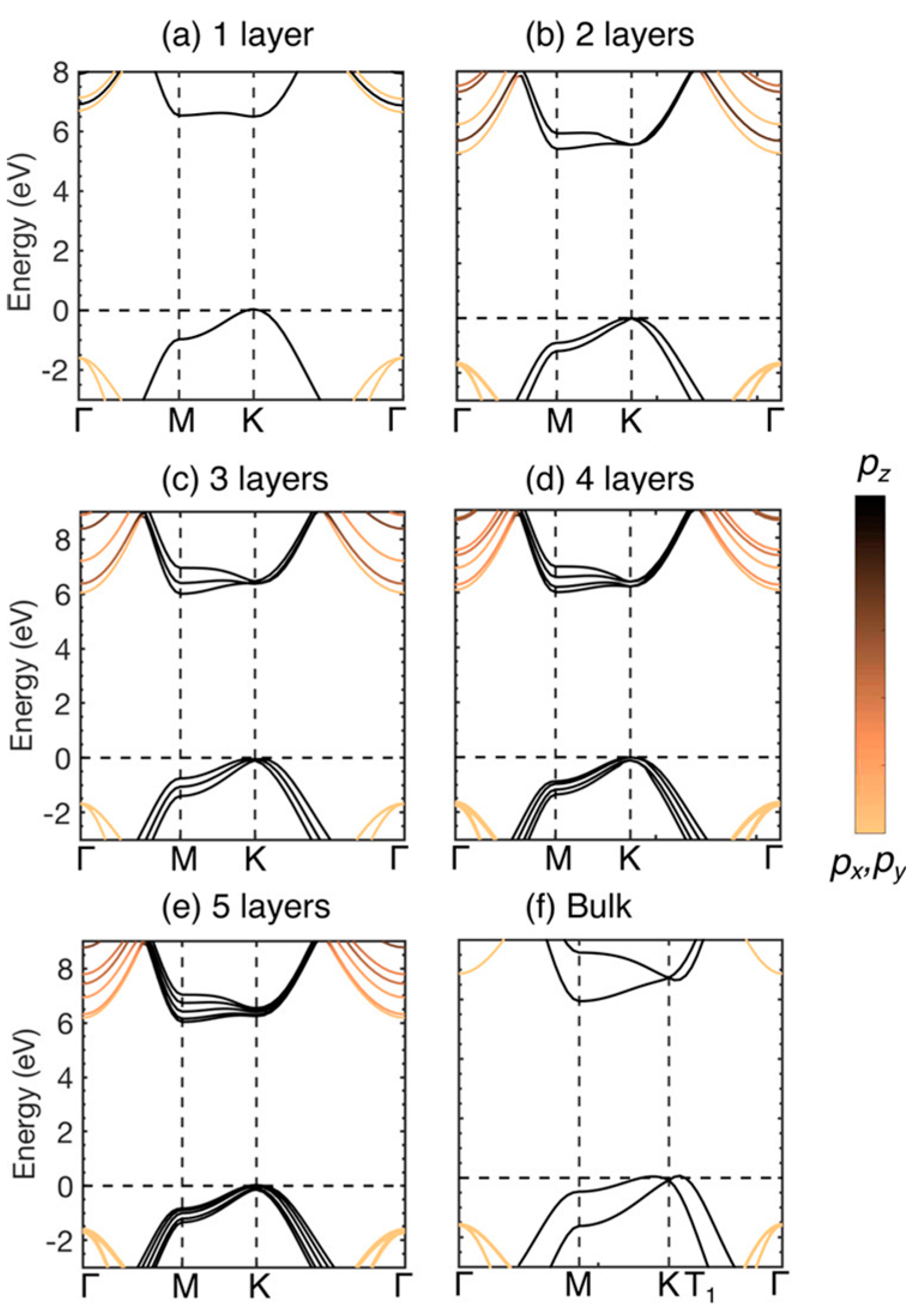
2.1. Electronic Bandgap Structure

The bandgap structure of hBN has long been debated. Theoretical calculations, such as first-principles calculations, show that it should have an indirect bandgap structure [15,16,17,18], whereas experimental results using optical microscopy indicate that the obtained optical properties are caused by a direct bandgap [19,20,21]. For example, Watanabe et al. fabricated high-purity hBN crystals and observed an intense luminescence peak at 5.76 eV under UV irradiation, which they attributed to a direct bandgap [20]. This issue was ultimately resolved using two-photon excitation, which revealed that multilayer hBN has an indirect bandgap at 5.955 eV [22]. Its intense luminescence is attributed to strong exciton–phonon interactions that produce self-trapped exciton states owing to the vdW structure of hBN [23].
As shown in Figure 3, the bandgap structure of hBN strongly depends on the layer number [24]. The bandgap structure was investigated by first-principles calculations. Monolayer hBN exhibits a direct bandgap; however, when the layer number is greater than or equal to two, hBN exhibits an indirect bandgap. This bandgap structure means that hBN can be applied in devices such as light-emitting diodes (LEDs) and photodetectors (PDs) operating in the DUV wavelength region. Furthermore, monolayer hBN is a promising platform for polariton manipulation in the UV range [25].

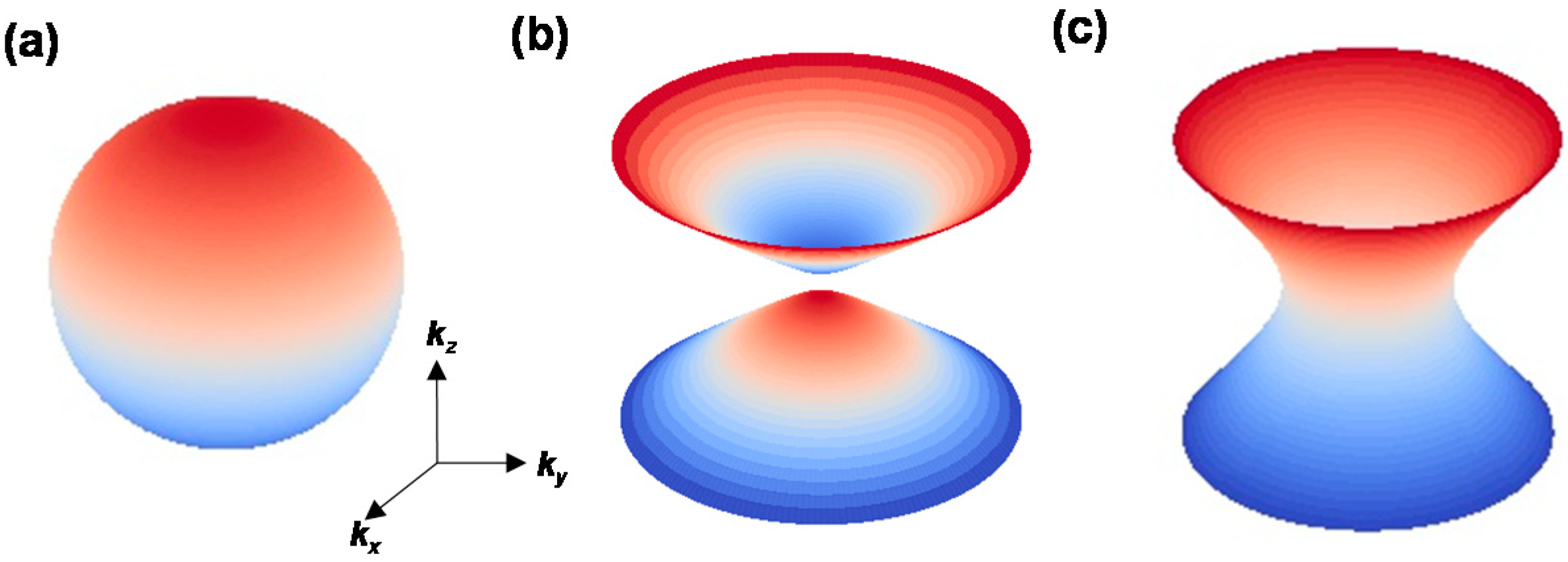
2.2. Asymmetric Permittivities

hBN has two anisotropic permittivities, ε and ε, which correspond to two types of phonon modes: (i) an out-of-plane (‖) mode with a transverse optical frequency (ωTO) of 780 cm−1 and longitudinal optical phonon frequency (ωLO) of 830 cm−1, and (ii) an in-plane (⊥) mode with a ωTO of 1370 cm−1 and ωLO of 1610 cm−1 [26]. Accordingly, the anisotropic permittivity of hBN is defined by [26]:
ϵ m = ϵ ,   m + ϵ ,   m × ( ω LO ,   m ) 2 ( ω TO ,   m ) 2 ( ω TO ,   m ) 2 ω 2 i ω Γ m ,
where ε and Γ are the high-frequency dielectric permittivity and damping constant, respectively; m = ‖ and ⊥; ε∞,⊥ = 4.87, ε∞,‖ = 2.95, Γ = 5 cm−1, and Γ = 4 cm−1 [27]; and ω is the wave frequency.
The two anisotropic permittivities are the origin of the unique HPPs of hBN. Figure 4a,b show the real and imaginary parts of the permittivities of hBN, respectively. Two distinct types of reststrahlen (RS) bands are formed, in which the permittivities ε and ε have opposite signs. Type-I (where ε < 0 and ε > 0) occurs in the frequency range of 746–819 cm−1 and wavelength range of 12.21–13.4 μm, whereas Type-II (where ε < 0 and ε > 0) occurs in the frequency range of 1370–1610 cm−1 and wavelength range of 6.21–7.30 μm. Therefore, hBN has HPPs in these two RS bands in the IR region at approximately 7 and 13 μm.
In these hyperbolic regions, the isofrequency surface with z as the optical axis is defined by [28]:
k x 2 + k y 2 ϵ + k z 2 ϵ = ( ω c ) 2 ,
where kx, ky, and kz are the wavevectors of the x, y, and z axes, respectively, and c is the speed of light in vacuum. Figure 5a–c show the isofrequency surfaces of non-hyperbolic materials (ε = ε < 0), Type-I hyperbolic materials (ε < 0, ε > 0), and Type-II hyperbolic materials (ε < 0, ε > 0), respectively.
The energy propagation direction of polaritons, defined by the angle β between the Poynting vector and z-axis, is defined by [29]:
β ( ω ) = arctan ( i ϵ ( ω ) ϵ ( ω ) ) .
In some cases, Equation (3) is expressed as [28,30]:
β ( ω ) = π 2 arctan ( ϵ ( ω ) i ϵ ( ω ) ) .
As shown in Figure 5 and Equations (3) and (4), these hyperbolic regions allow kx and ky to become infinitely large in hBN, enabling light to be folded within the material. This is the origin of the strong light confinement in extremely small volumes of hBN [28,31] and its ability to realize sub-diffraction imaging [29,32]. Such HPPs have been directly observed in both multilayer [33,34] and monolayer [35] hBN using near-field microscopy. Furthermore, inducing curvature in hBN structures has been shown to modify the HPPs [36,37]. Controlling the thickness (layer number) and shape of hBN is critical for the development of next-generation HPP-based photonic devices.
It should be noted that orthorhombic-phase molybdenum trioxide (α-MoO3), which is another vdW material, also exhibits HPPs in the IR region [38,39,40].

3. Ultraviolet Devices

Because the bandgap of hBN lies in the DUV region, hBN has excellent potential for the design of DUV-LEDs and DUV-PDs. These applications are discussed in this section.

3.1. DUV-LEDs

DUV-LEDs have attracted considerable attention for a wide range of applications, including sterilization, water purification, photocatalysis, and curing. In particular, interest in UV disinfection technologies has rapidly grown owing to the COVID-19 pandemic [41].
AlGaN semiconductors are the most widely investigated materials for fabricating DUV-LEDs [42]. hBN was initially introduced as an electron-blocking and p-contact layer to enhance the hole injection efficiency, reduce the contact resistance, and increase the UV transparency of AlGaN-based LEDs. However, AlGaN-based DUV-LEDs emit light perpendicular to the surface plane [43], whereas the light emitted from hBN is parallel to the surface plane. Furthermore, hBN can be formed on arbitrary substrates with high DUV transparency owing to the vdW forces of hBN. Therefore, hBN is considered an efficient emissive layer for use in DUV-LEDs.
Multilayer hBN can produce strong photoluminescence [22,44] and cathodoluminescence [20,21,44,45,46] in the DUV region despite its indirect bandgap. This phenomenon is attributed to the strong coupling of the exciton–phonon interactions [46]. Such phonon-assisted recombination is fast enough (~100 ps) to bypass non-radiative relaxation [44,47]. Consequently, the internal quantum efficiency is comparable to that of semiconductors with a direct bandgap [46]. Thus, hBN has the advantages of both direct and indirect bandgap semiconductors, which helps to achieve both a high extraction efficiency and internal quantum efficiency.
The electroluminescence of hBN in the DUV region has not been demonstrated thus far. Recently, the electroluminescence of a graphene/hBN/graphene vdW heterostructure was demonstrated at room temperature (Figure 6) [48]. The graphene/hBN/graphene vdW heterostructure (Figure 6a), in which the photoactive layer of hBN was sandwiched between a pair of graphene layers as electrodes, was fabricated from exfoliated graphene and hBN via a dry transfer technique. Carrier injection from the graphene electrodes to the hBN band edges occurred under high bias voltages via Fowler–Nordheim tunneling.
Figure 6b shows the electroluminescence spectra of the graphene/hBN/graphene vdW heterostructure under a forward bias at various currents, and Figure 6c shows the dependence of the electroluminescence external quantum efficiency (EQE) on the current under forward and reverse biases. The EQE gradually increased with the increasing current. The difference between the two bias polarities stems from asymmetric charge carrier injection owing to the asymmetric shape of the device. The obtained EQE was low; however, it could be improved by using a symmetric device structure with balanced carrier injection, a blocking layer, and multiple emissive layers. In particular, the formation of p–n junctions is important for achieving high-performance hBN-based DUV optoelectronics. p-type doping has been achieved by introducing Mg dopant atoms [49,50,51] or B vacancies [52]. Recently, n-type doping has also been demonstrated by Ge–O doping [53]. Along with other 2D materials, such technologies and suitable fabrication methods can help to realize highly efficient and stable DUV-LEDs.

3.2. DUV-PDs

Various UV-PDs have been developed from materials including AlGaN/GaN-based semiconductors [54,55], SiC-based semiconductors [56,57], oxide-based materials [58,59], and 2D materials [60] to cater to a wide range of applications, including advanced communications technologies, flare detection systems, and air purification devices [61].
Owing to its bandgap in the DUV region, various hBN-based UV-PDs have been developed [62,63,64]. Among them, hBN/Cu Schottky junctions and hBN/graphene vdW heterostructures have achieved substantially higher responsivities than single-hBN-based PDs. In particular, the photogating effect used in PDs based on hBN/graphene vdW heterostructures has recently drawn considerable research attention [65,66,67,68]. In these devices, hBN surrounds the graphene layer and acts as a photosensitizer by producing a voltage change upon light irradiation. Owing to the high carrier mobility and low atomic thickness of graphene, this voltage change can produce an extraordinary change in the carrier density of graphene [69]. As a result, the photocurrent can change significantly.
Figure 7a,b respectively show a schematic and image of a photogated hBN/graphene DUV-PD [70]. The PD structure is based on a simple graphene-based field effect transistor (GFETs). hBN is placed under the graphene channel and acts as a photosensitizer. It produces a back-gate voltage change in the GFET under DUV light irradiation, enabling the current in the graphene channel to be modulated substantially. Figure 7c shows the photo current and responsivity as a function of the source–drain voltage for DUV-PDs with and without hBN. The results demonstrate that ultra-high responsivity can be achieved by photogating.
As discussed in Section 3.1, the realization of hBN p–n junctions can facilitate the development of high-performance DUV-PDs, which cannot be achieved with conventional UV-PD technologies. In addition, the development of electrical readout circuits suitable for hBN would enable the fabrication of DUV-based image sensors.

4. Perfect Infrared Absorbers/Emitters

In addition to its performance in the DUV wavelength region, hBN has a distinguished potential for use in photonic devices operating in the infrared (IR) region. Metamaterial/metasurface-inspired or plasmonics-inspired “perfect” IR absorbers and emitters [71,72] have emerged as key materials for use in radiative cooling [73,74], advanced functional IR sensors [75], and biosensing [76] applications. hBN is a promising material for small and highly efficient absorbers and emitters because it is a natural hyperbolic material in the IR region, which allows photons to be confined within an ultra-small volume of hBN.
The thermal radiation and absorbance of hBN can be controlled by adjusting the layer number [77]. Figure 8 shows unit cells of several hBN-based metasurface absorbers/emitters (hBN-MAEs) based on the well-known metal–insulator–metal (MIM) metasurface structure. Figure 8a shows the simplest hBN-MAE structure, in which rectangular blocks of hBN are placed periodically on a metal plate [78]. The most commonly used metals are Au, Ag, or Al because these metals support surface plasmon resonance (SPR). Figure 8b shows a slightly more complex structure, in which the sides of the hBN blocks are tapered [78]. Figure 8c shows an hBN-MAE in which a multilayer MIM pattern is introduced [79]. Finally, Figure 8d shows a structure in which hBN is placed on a metal grate [80,81,82]. Notably, devices with these structures have been shown to be promising IR absorbers/emitters.
Here, the basic absorption properties of hBN due to the HPPs are explained with consideration to the simplest hBN-MAE structure, that is, the rectangular hBN/metal structure (Figure 8a). Figure 9a shows a schematic of the device and its absorption spectrum. Figure 9b shows the power dissipation contours at wavelengths of 6.29, 6.41, and 6.56 μm, which correspond to the absorption peaks in the absorption spectrum (Figure 9a) in the Type-II hyperbolic region. Figure 9b clearly shows three zigzag resonant modes, demonstrating the strong confinement of light inside hBN owing to the HPPs. The resonance modes at wavelengths of 6.29, 6.41, and 6.56 μm are defined as (m, n) = (3, 1), (3, 2), and (3, 3), respectively.
Based on these resonance modes, the propagation direction can be described by [78]:
tan β = n m .
Notably, this equation is important in the design of hBN-based photonic devices using HPPs. This is because the resonance modes are defined by the aspect ratio of the hBN cavity and not by its overall shape. This is a unique property of HPPs and is not observed with conventional resonance such as Fabry–Pérot resonance [28,83].
Figure 9c–e respectively show a schematic of the trapezoidal hBN/metal structure, its absorption spectrum, and its absorbance as a function of the incident angle and wavelength. As shown in Figure 9c, in the trapezoidal hBN resonator, β can be modified based on the taper angle, leading to broader absorption.
The combination of SPR and HPPs can enhance the unique absorption properties of hBN. The multilayer hBN/metal structure shown in Figure 8c can produce broadband absorption owing to the SPR induced by the metal and the resulting hybridization of HPPs [79]. In addition, when hBN is placed on a Ag-based one-dimensional (1D) plasmonic grating, as shown schematically in Figure 8d and Figure 10a, it exhibits enhanced absorption due to coupling between the HPPs of hBN and the SPR or magnetic polaritons induced by the 1D plasmonic grating [84,85,86]. Figure 10b,c show the electric field distributions of hBN on 1D plasmonic gratings with different groove widths. Zigzag propagation modes were induced within the hBN layer owing to coupling between the magnetic polaritons induced by the 1D plasmonic grating and the HPPs of hBN. Because the hyperbolic properties follow Equations (3) or (4), the change in coupling frequency with groove width is minimal.
Plasmonic structures such as 2D plasmonic crystals and asymmetric structures [87,88] can be used to enhance the interaction between SPR induced by the plasmonic structure and the HPPs in hBN. This enhanced interaction can facilitate the design of novel photonic devices that employ IR absorption and emission. In addition to the aforementioned IR absorbers/emitters, hBN is frequently used in graphene-based metamaterial IR absorbers/emitters [89,90,91,92,93]; the use of patterned graphene can result in strong absorption induced by localized SPR in the IR region [94,95].

5. Sub-Diffraction-Limit Imaging

Hyperbolic materials allow large wavevector (k) values. In hyperlenses, the light scattered from sub-diffraction-limit features is coupled with the HPPs, which propagates the light in the expanded direction according to Equation (3). As a result, sub-diffraction-limit imaging can be achieved.
Early research into hyperlenses used hyperbolic metamaterials (HMMs) with artificially engineered structures [96,97] to demonstrate hyperlenses or superlenses [98,99,100]. However, conventional HMMs require complicated artificial structures such as multilayers of dielectric and metal films. Furthermore, metal films induce optical loss for imaging. Therefore, hyperlenses using HMMs suffer from a low transmission efficiency and limited spatial resolution [101,102]. On the contrary, hBN is a natural hyperbolic material with low-loss HPPs in two RS bands. Therefore, hBN is suitable for the development of high-performance hyperlenses.
A schematic of a hBN-based hyperlens is shown in Figure 11a. The hyperlens was demonstrated with Au disks embedded in hBN [29,32] and visualized by scattering-type scanning near-field optical microscopy (s-SNOM). HPPs propagate light from the edges of the Au disks under IR illumination. Figure 11c,d show the electric field distribution in the z direction for hBN-based hyperlenses with different aspect ratios (a/d, where d is the thickness of the hBN film and a is the radius of the Au disk) and propagation directions (θ) [29]. Here, θ corresponds to β in Equations (3) and (4). These calculated results demonstrate that the unique zigzag propagation of the HPPs enables the hyperlens behavior and the aspect ratio a/d defines the propagation mode. Figure 11e shows an atomic force microscopy (AFM) image of the Au nanodisks and Figure 11f–h show s-SNOM images of the Au nanodisks taken at IR laser frequencies within, at the boundary of, and outside the hyperbolic region, respectively. These figures clearly show that sub-diffraction-limit imaging with a resolution of λ/33 was achieved in the Type-II hyperbolic region.
hBN-based hyperlenses have been used for various applications, including in defect diagnosis [103]. Furthermore, compared with naturally abundant hBN, the use of monoisotopic h11BN (>99%) [104] has been shown to reduce optical losses by a factor of three and an imaging resolution of at least λ/154 was achieved [102]. Moreover, a graphene/hBN multilayer hypercrystal achieved high-efficiency negative transmission, which can promote superlens imaging at high resolutions. Therefore, hBN-based hyperlenses have promising applications in biomedical imaging, internal structure diagnosis, label-free detection, and fine-structure analysis.

6. HPP-Based Sensors

IR spectroscopy is a powerful analytical tool for label-free and non-destructive material characterization based on the unique fingerprints of molecules. In particular, surface-enhanced IR absorption (SEIRA) spectroscopy is promising for high-precision material analysis [105]. SEIRA spectroscopy is based on the strong interaction between IR light and molecules in the strongly confined near field of localized SPRs (LSPRs). However, in conventional SEIRA spectroscopy, noble metals such as Au are used to produce LSPRs, which inevitably involves losses, and the quality factor (Q) therein is limited to ~10 [106]. In addition, although graphene-based LSPRs can be tuned by doping, the resultant Q is poor [107].
In contrast, because the HPPs of hBN can confine IR light to a small cavity, hBN can achieve a high Q of ~100 [104]. Therefore, hBN is a strong candidate for SEIRA spectroscopy. 4,4′-Bis(N-carbazolyl)-1,1′-biphenyl and CO2 sensing using hBN nanoribbons have been demonstrated previously [108,109]. Figure 12a schematically shows the CO2 gas sensing setup and cross-section of the CO2-sensing chip using hBN nanoribbons. In this device, the blueshift of the HPPs in the Type-II hyperbolic region increases with increasing CO2 concentration, as shown in Figure 12b,c, thereby enabling CO2 sensing [109].
For advanced SEIRA spectroscopy, hBN with tunable HPPs based on graphene and a 1D plasmonic grating has been proposed [82]. The electrical gating enables control over the Fermi level of graphene, which thus provides electrical tunability to hBN. The high Q of high-quality hBN and electrical tunability of graphene could contribute to the development of next-generation biosensing devices.

7. Future Outlook

hBN has excellent potential for use in photonic devices that operate in both the DUV and IR wavelength regions owing to its unique bandgap structure and the hyperbolicity of its dielectric constant. In addition to the applications discussed in this review, various other applications of hBN-based photonic devices have been proposed, including ultra-thin wavelength-selective filters [110], waveguides [111,112,113,114], and photonic crystals [115].
The rapid progress in the fabrication of hBN-based p–n junctions is expected to enable the development of high-performance DUV-LEDs and DUV-PDs in the near future. In the IR wavelength region, the artificial control of HPPs is crucial for the development of novel photonic devices, including thermal control devices [116,117]. Engineered surfaces such as metasurfaces [118,119,120] and waveguides [121] are crucial for controlling the HPPs. Graphene/hBN hybrids can afford HPP tunability for tunable IR photonic devices [26,122,123]. Moreover, the concept of topological photonics [124] is expected to broaden the field of HPP-based photonic devices.
Stacking layer angle control, as in “twistronics,” is a unique method of bandgap structure engineering that can produce novel properties, such as DUV emission band modification [125], ferroelectricity [126], and color center tunability [127]. Furthermore, similar to turbostratic graphene, turbostratic hBN is expected to exhibit the properties of monolayer hBN even in multilayer structures [128,129].
The crucial issues pertaining to the development of hBN-based photonic devices include the fabrication of hBN, its transfer to an arbitrary substrate, and its compatibility with complementary metal-oxide semiconductor (CMOS) technologies [130,131,132]. These issues are also commonly encountered for other 2D materials used to fabricate electric and photonic devices. Owing to the difficulty in fabricating high-quality hBN films, the excellent properties of hBN- and hBN/graphene-based devices have been demonstrated using exfoliated hBN. Therefore, it is crucial to develop mass fabrication technologies for the production of high-quality hBN films, such as by using chemical vapor deposition (CVD) and transferring the prepared film onto an arbitrary substrate. Among the various CVD techniques [133,134,135], the seamless CVD fabrication of graphene/hBN interfaces is the most important [136,137], because wet transfer processes inevitably introduce contamination at the hBN/graphene interface. This contamination degrades the high carrier mobility of graphene, even with a high-quality hBN film. Superior etching techniques are also needed, because conventional etching techniques degrade the quality of hBN [138], thereby hindering the development of high-performance hBN-based photonic devices. Recent progress in the fabrication of 2D materials is expected to enable the production of high-quality hBN that could be compatible with CMOS technologies.

8. Conclusions

Herein, we reviewed the applications of hBN-based photonic devices based on two unique properties of hBN, namely, the indirect bandgap in the DUV wavelength region and the HPPs in the IR wavelength region. The development of DUV-LEDs and DUV-PDs, which exploit the unique indirect bandgap structure of hBN, is in the initial stage. However, p- and n-type doping and photogating effects can considerably improve their performance. The HPPs of hBN have been employed in numerous applications, including IR absorbers/emitters, hyperlenses, and SEIRA sensing devices. The HPPs enable IR light to be confined to ultra-small volumes within hBN, which facilitates wavelength-selective and broadband absorption and emission. The HPPs enable hBN to be employed in the development of hyperlenses owing to the large k vector. The strong localized fields of HPPs result in a high Q value, which facilitates SEIRA spectroscopy for molecule or gas sensing. Given the importance of hBN, its fabrication methods, such as CVD, must be drastically improved. A breakthrough in the fabrication technologies is expected to enable the mass production of high-performance hBN-based photonic devices. Photonic devices operating in the UV and IR wavelength regions have growing applications in security and everyday life. This review is expected to contribute to the development of hBN-based photonic devices and widen their applications.

Funding

This research received no external funding.

Institutional Review Board Statement

Not applicable.

Data Availability Statement

No new data were created or analyzed in this study.

Conflicts of Interest

The authors declare no conflict of interest.

References

  1. Ben, J.; Liu, X.; Wang, C.; Zhang, Y.; Shi, Z.; Jia, Y.; Zhang, S.; Zhang, H.; Yu, W.; Li, D.; et al. 2D III-Nitride Materials: Properties, Growth, and Applications. Adv. Mater. 2021, 33, 2006761. [Google Scholar] [CrossRef]
  2. Merlo, A.; Mokkapati, V.R.S.S.; Pandit, S.; Mijakovic, I. Boron nitride nanomaterials: Biocompatibility and bio-applications. Biomater. Sci. 2018, 6, 2298–2311. [Google Scholar] [CrossRef] [Green Version]
  3. Dean, C.R.; Young, A.F.; Meric, I.; Lee, C.; Wang, L.; Sorgenfrei, S.; Watanabe, K.; Taniguchi, T.; Kim, P.; Shepard, K.L.; et al. Boron nitride substrates for high-quality graphene electronics. Nat. Nanotechnol. 2010, 5, 722–726. [Google Scholar] [CrossRef]
  4. Woessner, A.; Lundeberg, M.B.; Gao, Y.; Principi, A.; Alonso-González, P.; Carrega, M.; Watanabe, K.; Taniguchi, T.; Vignale, G.; Polini, M.; et al. Highly confined low-loss plasmons in graphene–boron nitride heterostructures. Nat. Mater. 2015, 14, 421–425. [Google Scholar] [CrossRef] [Green Version]
  5. Wang, J.; Ma, F.; Liang, W.; Wang, R.; Sun, M. Optical, photonic and optoelectronic properties of graphene, h-BN and their hybrid materials. Nanophotonics 2017, 6, 943–976. [Google Scholar] [CrossRef]
  6. Caldwell, J.D.; Aharonovich, I.; Cassabois, G.; Edgar, J.H.; Gil, B.; Basov, D.N. Photonics with hexagonal boron nitride. Nat. Rev. Mater. 2019, 4, 552–567. [Google Scholar] [CrossRef]
  7. Li, L.H.; Chen, Y. Atomically Thin Boron Nitride: Unique Properties and Applications. Adv. Func. Mater. 2016, 26, 2594–2608. [Google Scholar] [CrossRef] [Green Version]
  8. Low, T.; Chaves, A.; Caldwell, J.D.; Kumar, A.; Fang, N.X.; Avouris, P.; Heinz, T.F.; Guinea, F.; Martin-Moreno, L.; Koppens, F. Polaritons in layered two-dimensional materials. Nat. Mater. 2017, 16, 182–194. [Google Scholar] [CrossRef] [Green Version]
  9. Revabhai, P.M.; Singhal, R.K.; Basu, H.; Kailasa, S.K. Progress on boron nitride nanostructure materials: Properties, synthesis and applications in hydrogen storage and analytical chemistry. J. Nanostruct. Chem. 2022, 13, 1–41. [Google Scholar] [CrossRef]
  10. Maestre, C.; Toury, B.; Steyer, P.; Garnier, V.; Journet, C. Hexagonal boron nitride: A review on selfstanding crystals synthesis towards 2D nanosheets. J. Phys. Mater. 2021, 4, 044018. [Google Scholar] [CrossRef]
  11. Geim, A.K.; Grigorieva, I.V. Van der Waals heterostructures. Nature 2013, 499, 419–425. [Google Scholar] [CrossRef] [Green Version]
  12. Novoselov, K.S.; Mishchenko, A.; Carvalho, A.; Castro Neto, A.H. 2D materials and van der Waals heterostructures. Science 2016, 353, aac9439. [Google Scholar] [CrossRef] [Green Version]
  13. Shaik, A.B.D.; Palla, P. Optical quantum technologies with hexagonal boron nitride single photon sources. Sci. Rep. 2021, 11, 12285. [Google Scholar] [CrossRef]
  14. Kubanek, A. Coherent Quantum Emitters in Hexagonal Boron Nitride. Adv. Quantum Technol. 2022, 5, 2200009. [Google Scholar] [CrossRef]
  15. Xu, Y.N.; Ching, W.Y. Calculation of ground-state and optical properties of boron nitrides in the hexagonal, cubic, and wurtzite structures. Phys. Rev. B 1991, 44, 7787–7798. [Google Scholar] [CrossRef]
  16. Furthmüller, J.; Hafner, J.; Kresse, G. Ab initio calculation of the structural and electronic properties of carbon and boron nitride using ultrasoft pseudopotentials. Phys. Rev. B 1994, 50, 15606–15622. [Google Scholar] [CrossRef]
  17. Blase, X.; Rubio, A.; Louie, S.G.; Cohen, M.L. Quasiparticle band structure of bulk hexagonal boron nitride and related systems. Phys. Rev. B 1995, 51, 6868–6875. [Google Scholar] [CrossRef]
  18. Arnaud, B.; Lebègue, S.; Rabiller, P.; Alouani, M. Huge excitonic effects in layered hexagonal boron nitride. Phys. Rev. Lett. 2006, 96, 026402. [Google Scholar] [CrossRef] [Green Version]
  19. Zunger, A.; Katzir, A.; Halperin, A. Optical properties of hexagonal boron nitride. Phys. Rev. B 1976, 13, 5560–5573. [Google Scholar] [CrossRef]
  20. Watanabe, K.; Taniguchi, T.; Kanda, H. Direct-bandgap properties and evidence for ultraviolet lasing of hexagonal boron nitride single crystal. Nat. Mater. 2004, 3, 404–409. [Google Scholar] [CrossRef]
  21. Kubota, Y.; Watanabe, K.; Tsuda, O.; Taniguchi, T. Deep ultraviolet light-emitting hexagonal boron nitride synthesized at atmospheric pressure. Science 2007, 317, 932–934. [Google Scholar] [CrossRef] [Green Version]
  22. Cassabois, G.; Valvin, P.; Gil, B. Hexagonal boron nitride is an indirect bandgap semiconductor. Nat. Photon. 2016, 10, 262–266. [Google Scholar] [CrossRef] [Green Version]
  23. Watanabe, K.; Taniguchi, T. Jahn-Teller effect on exciton states in hexagonal boron nitride single crystal. Phys. Rev. B 2009, 79, 193104. [Google Scholar] [CrossRef]
  24. Wickramaratne, D.; Weston, L.; Van de Walle, C.G. Monolayer to Bulk Properties of Hexagonal Boron Nitride. J. Phys. Chem. C 2018, 122, 25524–25529. [Google Scholar] [CrossRef]
  25. Ferreira, F.; Chaves, A.J.; Peres, N.M.R.; Ribeiro, R.M. Excitons in hexagonal boron nitride single-layer: A new platform for polaritonics in the ultraviolet. J. Opt. Soc. Am. B 2019, 36, 674–683. [Google Scholar] [CrossRef] [Green Version]
  26. Kumar, A.; Low, T.; Fung, K.H.; Avouris, P.; Fang, N.X. Tunable Light-Matter Interaction and the Role of Hyperbolicity in Graphene-hBN System. Nano Lett. 2015, 15, 3172–3180. [Google Scholar] [CrossRef]
  27. Cai, Y.; Zhang, L.; Zeng, Q.; Cheng, L.; Xu, Y. Infrared reflectance spectrum of BN calculated from first principles. Solid State Commun. 2007, 141, 262–266. [Google Scholar] [CrossRef] [Green Version]
  28. Caldwell, J.D.; Kretinin, A.V.; Chen, Y.; Giannini, V.; Fogler, M.M.; Francescato, Y.; Ellis, C.T.; Tischler, J.G.; Woods, C.R.; Giles, A.J.; et al. Sub-diffractional volume-confined polaritons in the natural hyperbolic material hexagonal boron nitride. Nat. Commun. 2014, 5, 5221. [Google Scholar] [CrossRef] [Green Version]
  29. Dai, S.; Ma, Q.; Andersen, T.; McLeod, A.S.; Fei, Z.; Liu, M.K.; Wagner, M.; Watanabe, K.; Taniguchi, T.; Thiemens, M.; et al. Subdiffractional focusing and guiding of polaritonic rays in a natural hyperbolic material. Nat. Commun. 2015, 6, 6963. [Google Scholar] [CrossRef] [Green Version]
  30. Giles, A.J.; Dai, S.; Glembocki, O.J.; Kretinin, A.V.; Sun, Z.; Ellis, C.T.; Tischler, J.G.; Taniguchi, T.; Watanabe, K.; Fogler, M.M.; et al. Imaging of Anomalous Internal Reflections of Hyperbolic Phonon-Polaritons in Hexagonal Boron Nitride. Nano Lett. 2016, 16, 3858–3865. [Google Scholar] [CrossRef] [Green Version]
  31. Tamagnone, M.; Ambrosio, A.; Chaudhary, K.; Jauregui, L.A.; Kim, P.; Wilson, W.L.; Capasso, F. Ultra-confined mid-infrared resonant phonon polaritons in van der Waals nanostructures. Sci. Adv. 2018, 4, eaat7189. [Google Scholar] [CrossRef] [Green Version]
  32. Li, P.; Lewin, M.; Kretinin, A.V.; Caldwell, J.D.; Novoselov, K.S.; Taniguchi, T.; Watanabe, K.; Gaussmann, F.; Taubner, T. Hyperbolic phonon-polaritons in boron nitride for near-field optical imaging and focusing. Nat. Commun. 2015, 6, 7507. [Google Scholar] [CrossRef] [Green Version]
  33. Dai, S.; Fei, Z.; Ma, Q.; Rodin, A.S.; Wagner, M.; McLeod, A.S.; Liu, M.K.; Gannett, W.; Regan, W.; Watanabe, K.; et al. Tunable Phonon Polaritons in Atomically Thin van der Waals Crystals of Boron Nitride. Science 2014, 343, 1125–1129. [Google Scholar] [CrossRef] [Green Version]
  34. Dai, S.; Tymchenko, M.; Yang, Y.; Ma, Q.; Pita-Vidal, M.; Watanabe, K.; Taniguchi, T.; Jarillo-Herrero, P.; Fogler, M.M.; Alu, A.; et al. Manipulation and Steering of Hyperbolic Surface Polaritons in Hexagonal Boron Nitride. Adv. Mater. 2018, 30, 1706358. [Google Scholar] [CrossRef] [Green Version]
  35. Dai, S.; Fang, W.; Rivera, N.; Stehle, Y.; Jiang, B.Y.; Shen, J.; Tay, R.Y.; Ciccarino, C.J.; Ma, Q.; Rodan-Legrain, D.; et al. Phonon Polaritons in Monolayers of Hexagonal Boron Nitride. Adv. Mater. 2019, 31, 1806603. [Google Scholar] [CrossRef] [Green Version]
  36. Zhou, Y.; Qi, D.X.; Wang, Y.K. Phonon polaritons in cylindrically curved h-BN. Opt. Express 2017, 25, 17606–17615. [Google Scholar] [CrossRef]
  37. Yan, X.; Li, J.; Gu, L.; Gadre, C.A.; Moore, S.L.; Aoki, T.; Wang, S.; Zhang, G.; Gao, Z.; Basov, D.N.; et al. Curvature-Induced One-Dimensional Phonon Polaritons at Edges of Folded Boron Nitride Sheets. Nano Lett. 2022, 22, 9319–9326. [Google Scholar] [CrossRef]
  38. Ma, W.; Alonso-González, P.; Li, S.; Nikitin, A.Y.; Yuan, J.; Martín-Sánchez, J.; Taboada-Gutiérrez, J.; Amenabar, I.; Li, P.; Vélez, S.; et al. In-plane anisotropic and ultra-low-loss polaritons in a natural van der Waals crystal. Nature 2018, 562, 557–562. [Google Scholar] [CrossRef] [Green Version]
  39. Zheng, Z.; Chen, J.; Wang, Y.; Wang, X.; Chen, X.; Liu, P.; Xu, J.; Xie, W.; Chen, H.; Deng, S.; et al. Highly Confined and Tunable Hyperbolic Phonon Polaritons in Van Der Waals Semiconducting Transition Metal Oxides. Adv. Mater. 2018, 30, 1705318. [Google Scholar] [CrossRef]
  40. Zheng, Z.; Xu, N.; Oscurato, S.L.; Tamagnone, M.; Sun, F.; Jiang, Y.; Ke, Y.; Chen, J.; Huang, W.; Wilson, W.L.; et al. A mid-infrared biaxial hyperbolic van der Waals crystal. Sci. Adv. 2019, 5, eaav8690. [Google Scholar] [CrossRef] [Green Version]
  41. Raeiszadeh, M.; Adeli, B. A Critical Review on Ultraviolet Disinfection Systems against COVID-19 Outbreak: Applicability, Validation, and Safety Considerations. ACS Photonics 2020, 7, 2941–2951. [Google Scholar] [CrossRef]
  42. Mondal, R.K.; Adhikari, S.; Chatterjee, V.; Pal, S. Recent advances and challenges in AlGaN-based ultra-violet light emitting diode technologies. Mater. Res. Bull. 2021, 140, 111258. [Google Scholar] [CrossRef]
  43. Jiang, H.X.; Lin, J.Y. Hexagonal boron nitride for deep ultraviolet photonic devices. Semicond. Sci. Technol. 2014, 29, 084003. [Google Scholar] [CrossRef]
  44. Watanabe, K.; Taniguchi, T.; Miya, K.; Sato, Y.; Nakamura, K.; Niiyama, T.; Taniguchi, M. Hexagonal boron nitride as a new ultraviolet luminescent material and its application—Fluorescence properties of hBN single-crystal powder. Diam. Relat. Mater. 2011, 20, 849–852. [Google Scholar] [CrossRef]
  45. Pierret, A.; Loayza, J.; Berini, B.; Betz, A.; Plaçais, B.; Ducastelle, F.; Barjon, J.; Loiseau, A. Excitonic recombinations in h−BN: From bulk to exfoliated layers. Phys. Rev. B 2014, 89, 035414. [Google Scholar] [CrossRef] [Green Version]
  46. Schué, L.; Sponza, L.; Plaud, A.; Bensalah, H.; Watanabe, K.; Taniguchi, T.; Ducastelle, F.; Loiseau, A.; Barjon, J. Bright Luminescence from Indirect and Strongly Bound Excitons in h-BN. Phys. Rev. Lett. 2019, 122, 067401. [Google Scholar] [CrossRef] [Green Version]
  47. Cassabois, G.; Valvin, P.; Gil, B. Intervalley scattering in hexagonal boron nitride. Phys. Rev. B 2016, 93, 035207. [Google Scholar] [CrossRef]
  48. Song, S.B.; Yoon, S.; Kim, S.Y.; Yang, S.; Seo, S.Y.; Cha, S.; Jeong, H.W.; Watanabe, K.; Taniguchi, T.; Lee, G.H.; et al. Deep-ultraviolet electroluminescence and photocurrent generation in graphene/hBN/graphene heterostructures. Nat. Commun. 2021, 12, 7134. [Google Scholar] [CrossRef]
  49. Dahal, R.; Li, J.; Majety, S.; Pantha, B.N.; Cao, X.K.; Lin, J.Y.; Jiang, H.X. Epitaxially grown semiconducting hexagonal boron nitride as a deep ultraviolet photonic material. Appl. Phys. Lett. 2011, 98, 211110. [Google Scholar] [CrossRef] [Green Version]
  50. Sun, F.; Hao, Z.; Liu, G.; Wu, C.; Lu, S.; Huang, S.; Liu, C.; Hong, Q.; Chen, X.; Cai, D.; et al. p-Type conductivity of hexagonal boron nitride as a dielectrically tunable monolayer: Modulation doping with magnesium. Nanoscale 2018, 10, 4361–4369. [Google Scholar] [CrossRef]
  51. Wang, Y.; Liu, G.; Lu, S.; Zhang, H.; Guo, B.; Du, G.; Chen, X.; Cai, D.; Kang, J. Enhancement of p-type conductivity of monolayer hexagonal boron nitride by driving Mg incorporation through low-energy path with N-rich condition. Appl. Phys. Lett. 2020, 116, 212101. [Google Scholar] [CrossRef]
  52. Laleyan, D.A.; Zhao, S.; Woo, S.Y.; Tran, H.N.; Le, H.B.; Szkopek, T.; Guo, H.; Botton, G.A.; Mi, Z. AlN/h-BN Heterostructures for Mg Dopant-Free Deep Ultraviolet Photonics. Nano Lett. 2017, 17, 3738–3743. [Google Scholar] [CrossRef]
  53. Lu, S.; Shen, P.; Zhang, H.; Liu, G.; Guo, B.; Cai, Y.; Chen, H.; Xu, F.; Zheng, T.; Xu, F.; et al. Towards n-type conductivity in hexagonal boron nitride. Nat. Commun. 2022, 13, 3109. [Google Scholar] [CrossRef]
  54. Tan, R.; Cai, Q.; Wang, J.; Pan, D.; Li, Z.; Chen, D. Highly solar-blind ultraviolet selective metal-semiconductor-metal photodetector based on back-illuminated AlGaN heterostructure with integrated photonic crystal filter. Appl. Phys. Lett. 2021, 118, 142105. [Google Scholar] [CrossRef]
  55. Jiang, K.; Sun, X.; Chen, Y.; Zhang, S.; Ben, J.; Chen, Y.; Zhang, Z.-H.; Jia, Y.; Shi, Z.; Li, D. Three-dimensional metal–semiconductor–metal bipolar ultraviolet phototransistor based on GaN p-i-n epilayer. Appl. Phys. Lett. 2021, 119, 161105. [Google Scholar] [CrossRef]
  56. Chen, X.; Zhu, H.; Cai, J.; Wu, Z. High-performance 4H-SiC-based ultraviolet p-i-n photodetector. J. Appl. Phys. 2007, 102, 024505. [Google Scholar] [CrossRef]
  57. Aldalbahi, A.; Li, E.; Rivera, M.; Velazquez, R.; Altalhi, T.; Peng, X.; Feng, P.X. A new approach for fabrications of SiC based photodetectors. Sci. Rep. 2016, 6, 23457. [Google Scholar] [CrossRef]
  58. Kim, S.; Kim, J. Highly selective ozone-treated β-Ga2O3 solar-blind deep-UV photodetectors. Appl. Phys. Lett. 2020, 117, 261101. [Google Scholar] [CrossRef]
  59. Han, D.; Liu, K.; Chen, X.; Li, B.; Zhai, T.; Liu, L.; Shen, D. Performance enhancement of a self-powered solar-blind UV photodetector based on ZnGa2O4/Si heterojunction via interface pyroelectric effect. Appl. Phys. Lett. 2021, 118, 251101. [Google Scholar] [CrossRef]
  60. Yu, Y.; Shen, T.; Long, H.; Zhong, M.; Xin, K.; Zhou, Z.; Wang, X.; Liu, Y.Y.; Wakabayashi, H.; Liu, L.; et al. Doping Engineering in the MoS(2) /SnSe(2) Heterostructure toward High-Rejection-Ratio Solar-Blind UV Photodetection. Adv. Mater. 2022, 34, 2206486. [Google Scholar] [CrossRef]
  61. Chen, H.; Liu, K.; Hu, L.; Al-Ghamdi, A.A.; Fang, X. New concept ultraviolet photodetectors. Mater. Today 2015, 18, 493–502. [Google Scholar] [CrossRef]
  62. Zhou, A.F.; Aldalbahi, A.; Feng, P. Vertical metal-semiconductor-metal deep UV photodetectors based on hexagonal boron nitride nanosheets prepared by laser plasma deposition. Opt. Mater. Express 2016, 6, 3286. [Google Scholar] [CrossRef]
  63. Veeralingam, S.; Durai, L.; Yadav, P.; Badhulika, S. Record-High Responsivity and Detectivity of a Flexible Deep-Ultraviolet Photodetector Based on Solid State-Assisted Synthesized hBN Nanosheets. ACS Appl. Electron. Mater. 2021, 3, 1162–1169. [Google Scholar] [CrossRef]
  64. Yang, H.; Wang, L.; Gao, F.; Dai, M.; Hu, Y.; Chen, H.; Zhang, J.; Qiu, Y.; Jia, C.; Zhou, Y.; et al. Shape evolution of two dimensional hexagonal boron nitride single domains on Cu/Ni alloy and its applications in ultraviolet detection. Nanotechnology 2019, 30, 245706. [Google Scholar] [CrossRef]
  65. Shimatani, M.; Ogawa, S.; Fujisawa, D.; Okuda, S.; Kanai, Y.; Ono, T.; Matsumoto, K. Giant Dirac point shift of graphene phototransistors by doped silicon substrate current. AIP Adv. 2016, 6, 035113. [Google Scholar] [CrossRef] [Green Version]
  66. Kufer, D.; Konstantatos, G. Photo-FETs: Phototransistors Enabled by 2D and 0D Nanomaterials. ACS Photonics 2016, 3, 2197–2210. [Google Scholar] [CrossRef] [Green Version]
  67. Guo, X.; Wang, W.; Nan, H.; Yu, Y.; Jiang, J.; Zhao, W.; Li, J.; Zafar, Z.; Xiang, N.; Ni, Z.; et al. High-performance graphene photodetector using interfacial gating. Optica 2016, 3, 1066–1070. [Google Scholar] [CrossRef]
  68. Shimatani, M.; Fukushima, S.; Okuda, S.; Ogawa, S. High-performance graphene/InSb heterojunction photodetectors for high-resolution mid-infrared image sensors. Appl. Phys. Lett. 2020, 117, 173102. [Google Scholar] [CrossRef]
  69. Ogawa, S.; Shimatani, M.; Fukushima, S.; Okuda, S.; Kanai, Y.; Ono, T.; Matsumoto, K. Broadband photoresponse of graphene photodetector from visible to long-wavelength infrared wavelengths. Opt. Eng. 2019, 58, 057106. [Google Scholar]
  70. Fukushima, S.; Fukamachi, S.; Shimatani, M.; Kawahara, K.; Ago, H.; Ogawa, S. Graphene-based deep-ultraviolet photodetectors with ultrahigh responsivity using chemical vapor deposition of hexagonal boron nitride to achieve photogating. Opt. Mater. Express 2022, 12, 2090–2101. [Google Scholar] [CrossRef]
  71. Watts, C.M.; Liu, X.; Padilla, W.J. Metamaterial electromagnetic wave absorbers. Adv. Mater. 2012, 24, OP98–OP120. [Google Scholar] [CrossRef] [PubMed]
  72. Ogawa, S.; Kimata, M. Metal-Insulator-Metal-Based Plasmonic Metamaterial Absorbers at Visible and Infrared Wavelengths: A Review. Materials 2018, 11, 458. [Google Scholar] [CrossRef] [PubMed] [Green Version]
  73. Zhai, Y.; Ma, Y.; David, S.N.; Zhao, D.; Lou, R.; Tan, G.; Yang, R.; Yin, X. Scalable-manufactured randomized glass-polymer hybrid metamaterial for daytime radiative cooling. Science 2017, 355, 1062–1066. [Google Scholar] [CrossRef] [PubMed] [Green Version]
  74. Ko, B.; Lee, D.; Badloe, T.; Rho, J. Metamaterial-Based Radiative Cooling: Towards Energy-Free All-Day Cooling. Energies 2018, 12, 89. [Google Scholar] [CrossRef] [Green Version]
  75. Ogawa, S.; Kimata, M. Wavelength- or Polarization-Selective Thermal Infrared Detectors for Multi-Color or Polarimetric Imaging Using Plasmonics and Metamaterials. Materials 2017, 10, 493. [Google Scholar] [CrossRef]
  76. Liu, N.; Mesch, M.; Weiss, T.; Hentschel, M.; Giessen, H. Infrared Perfect Absorber and Its Application as Plasmonic Sensor. Nano Lett. 2010, 10, 2342–2348. [Google Scholar] [CrossRef]
  77. Zhao, B.; Song, J.-H.; Brongersma, M.; Fan, S. Atomic-Scale Control of Coherent Thermal Radiation. ACS Photonics 2021, 8, 872–878. [Google Scholar] [CrossRef]
  78. Zhao, B.; Zhang, Z.M. Resonance perfect absorption by exciting hyperbolic phonon polaritons in 1D hBN gratings. Opt. Express 2017, 25, 7791–7796. [Google Scholar] [CrossRef] [Green Version]
  79. Kan, Y.H.; Zhao, C.Y.; Zhang, Z.M. Compact mid-infrared broadband absorber based on hBN/metal metasurface. Int. J. Therm. Sci. 2018, 130, 192–199. [Google Scholar] [CrossRef]
  80. Zhao, B.; Zhang, Z.M. Perfect mid-infrared absorption by hybrid phonon-plasmon polaritons in hBN/metal-grating anisotropic structures. Int. J. Heat Mass Transf. 2017, 106, 1025–1034. [Google Scholar] [CrossRef] [Green Version]
  81. Hu, J.; Xie, W.; Chen, J.; Zhou, L.; Liu, W.; Li, D.; Zhan, Q. Strong hyperbolic-magnetic polaritons coupling in an hBN/Ag-grating heterostructure. Opt. Express 2020, 28, 22095–22104. [Google Scholar] [CrossRef] [PubMed]
  82. Kumari, R.; Yadav, A.; Sharma, S.; Das Gupta, T.; Varshney, S.K.; Lahiri, B. Tunable Van der Waal’s optical metasurfaces (VOMs) for biosensing of multiple analytes. Opt. Express 2021, 29, 25800–25811. [Google Scholar] [CrossRef] [PubMed]
  83. Sun, Z.; Gutiérrez-Rubio, Á.; Basov, D.N.; Fogler, M.M. Hamiltonian Optics of Hyperbolic Polaritons in Nanogranules. Nano Lett. 2015, 15, 4455–4460. [Google Scholar] [CrossRef] [PubMed] [Green Version]
  84. Miyazaki, H.T.; Ikeda, K.; Kasaya, T.; Yamamoto, K.; Inoue, Y.; Fujimura, K.; Kanakugi, T.; Okada, M.; Hatade, K.; Kitagawa, S. Thermal emission of two-color polarized infrared waves from integrated plasmon cavities. Appl. Phys. Lett. 2008, 92, 141114. [Google Scholar] [CrossRef]
  85. Bouchon, P.; Pardo, F.; Portier, B.; Ferlazzo, L.; Ghenuche, P.; Dagher, G.; Dupuis, C.; Bardou, N.; Haïdar, R.; Pelouard, J.-L. Total funneling of light in high aspect ratio plasmonic nanoresonators. Appl. Phys. Lett. 2011, 98, 191109. [Google Scholar] [CrossRef]
  86. Ogawa, S.; Kimata, M. Direct fabrication and characterization of high-aspect-ratio plasmonic nanogratings using tapered-sidewall molds. Opt. Mater. Express 2017, 7, 633–640. [Google Scholar] [CrossRef]
  87. Ogawa, S.; Okada, K.; Fukushima, N.; Kimata, M. Wavelength selective uncooled infrared sensor by plasmonics. Appl. Phys. Lett. 2012, 100, 021111. [Google Scholar] [CrossRef]
  88. Ogawa, S.; Takagawa, Y.; Kimata, M. Fano resonance in asymmetric-period two-dimensional plasmonic absorbers for dual-band uncooled infrared sensors. Opt. Eng. 2016, 55, 117105. [Google Scholar] [CrossRef] [Green Version]
  89. Cai, Y.; Zhu, J.; Liu, Q.H. Tunable enhanced optical absorption of graphene using plasmonic perfect absorbers. Appl. Phys. Lett. 2015, 106, 043105. [Google Scholar] [CrossRef] [Green Version]
  90. Wu, J.; Jiang, L.; Guo, J.; Dai, X.; Xiang, Y.; Wen, S. Tunable perfect absorption at infrared frequencies by a graphene-hBN hyper crystal. Opt. Express 2016, 24, 17103–17114. [Google Scholar] [CrossRef]
  91. Hajian, H.; Ghobadi, A.; Butun, B.; Ozbay, E. Tunable, omnidirectional, and nearly perfect resonant absorptions by a graphene-hBN-based hole array metamaterial. Opt. Express 2018, 26, 16940–16954. [Google Scholar] [CrossRef] [PubMed]
  92. Deng, G.; Song, X.; Dereshgi, S.A.; Xu, H.; Aydin, K. Tunable multi-wavelength absorption in mid-IR region based on a hybrid patterned graphene-hBN structure. Opt. Express 2019, 27, 23576–23584. [Google Scholar] [CrossRef] [PubMed]
  93. Ogawa, S.; Fukushima, S.; Shimatani, M. Hexagonal-boron nitride/graphene van der Waals heterostructure-based wavelength-selective infrared absorbers using plasmonic metasurfaces for multi-spectral infrared photodetectors. J. Opt. Soc. Am. B 2022, 39, 3149–3158. [Google Scholar] [CrossRef]
  94. García de Abajo, F.J. Graphene Plasmonics: Challenges and Opportunities. ACS Photonics 2014, 1, 135–152. [Google Scholar] [CrossRef] [Green Version]
  95. Ogawa, S.; Fukushima, S.; Shimatani, M. Graphene Plasmonics in Sensor Applications: A Review. Sensors 2020, 20, 3563. [Google Scholar] [CrossRef] [PubMed]
  96. Poddubny, A.; Iorsh, I.; Belov, P.; Kivshar, Y. Hyperbolic metamaterials. Nat. Photonics 2013, 7, 948–957. [Google Scholar] [CrossRef]
  97. Takayama, O.; Lavrinenko, A.V. Optics with hyperbolic materials [Invited]. J. Opt. Soc. Am. B 2019, 36, F38–F48. [Google Scholar] [CrossRef] [Green Version]
  98. Liu, Z.; Lee, H.; Xiong, Y.; Sun, C.; Zhang, X. Far-field optical hyperlens magnifying sub-diffraction-limited objects. Science 2007, 315, 1686. [Google Scholar] [CrossRef] [Green Version]
  99. Rho, J.; Ye, Z.; Xiong, Y.; Yin, X.; Liu, Z.; Choi, H.; Bartal, G.; Zhang, X. Spherical hyperlens for two-dimensional sub-diffractional imaging at visible frequencies. Nat. Commun. 2010, 1, 143. [Google Scholar] [CrossRef] [Green Version]
  100. Kawata, S.; Inouye, Y.; Verma, P. Plasmonics for near-field nano-imaging and superlensing. Nat. Photonics 2009, 3, 388–394. [Google Scholar] [CrossRef]
  101. Lee, D.; Kim, Y.D.; Kim, M.; So, S.; Choi, H.-J.; Mun, J.; Nguyen, D.M.; Badloe, T.; Ok, J.G.; Kim, K.; et al. Realization of Wafer-Scale Hyperlens Device for Sub-diffractional Biomolecular Imaging. ACS Photonics 2018, 5, 2549–2554. [Google Scholar] [CrossRef]
  102. He, M.; Iyer, G.R.S.; Aarav, S.; Sunku, S.S.; Giles, A.J.; Folland, T.G.; Sharac, N.; Sun, X.; Matson, J.; Liu, S.; et al. Ultrahigh-Resolution, Label-Free Hyperlens Imaging in the Mid-IR. Nano Lett. 2021, 21, 7921–7928. [Google Scholar] [CrossRef]
  103. Dai, S.; Tymchenko, M.; Xu, Z.-Q.; Tran, T.T.; Yang, Y.; Ma, Q.; Watanabe, K.; Taniguchi, T.; Jarillo-Herrero, P.; Aharonovich, I.; et al. Internal Nanostructure Diagnosis with Hyperbolic Phonon Polaritons in Hexagonal Boron Nitride. Nano Lett. 2018, 18, 5205–5210. [Google Scholar] [CrossRef] [Green Version]
  104. Giles, A.J.; Dai, S.; Vurgaftman, I.; Hoffman, T.; Liu, S.; Lindsay, L.; Ellis, C.T.; Assefa, N.; Chatzakis, I.; Reinecke, T.L.; et al. Ultralow-loss polaritons in isotopically pure boron nitride. Nat. Mater. 2018, 17, 134–139. [Google Scholar] [CrossRef] [Green Version]
  105. Wang, H.L.; You, E.M.; Panneerselvam, R.; Ding, S.Y.; Tian, Z.Q. Advances of surface-enhanced Raman and IR spectroscopies: From nano/microstructures to macro-optical design. Light Sci. Appl. 2021, 10, 161. [Google Scholar] [CrossRef]
  106. Lilley, G.; Messner, M.; Unterrainer, K. Improving the quality factor of the localized surface plasmon resonance. Opt. Mater. Express 2015, 5, 2112–2120. [Google Scholar] [CrossRef]
  107. Rodrigo, D.; Limaj, O.; Janner, D.; Etezadi, D.; Abajo, F.J.G.d.; Pruneri, V.; Altug, H. Mid-infrared plasmonic biosensing with graphene. Science 2015, 349, 165–168. [Google Scholar] [CrossRef] [Green Version]
  108. Autore, M.; Li, P.; Dolado, I.; Alfaro-Mozaz, F.J.; Esteban, R.; Atxabal, A.; Casanova, F.; Hueso, L.E.; Alonso-González, P.; Aizpurua, J.; et al. Boron nitride nanoresonators for phonon-enhanced molecular vibrational spectroscopy at the strong coupling limit. Light Sci. Appl. 2018, 7, 17172. [Google Scholar] [CrossRef]
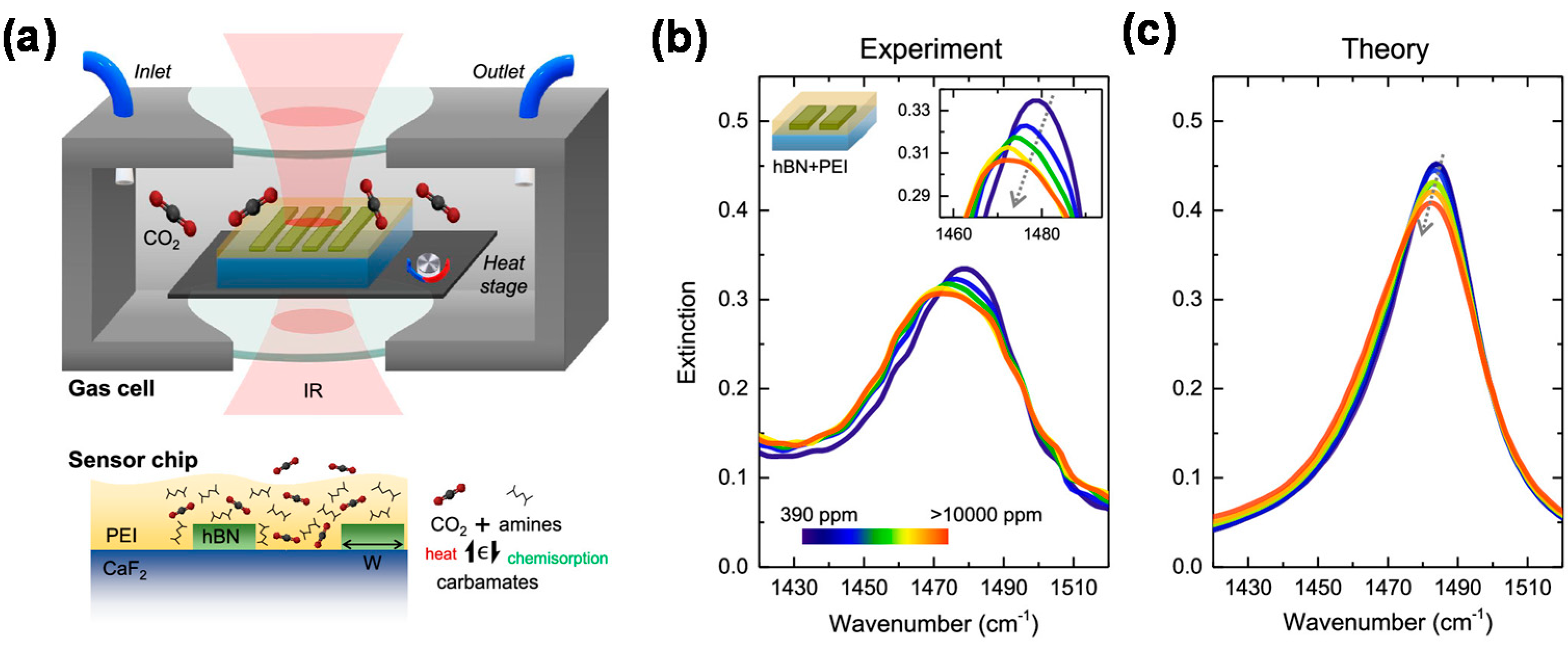
  109. Bareza, N., Jr.; Paulillo, B.; Slipchenko, T.M.; Autore, M.; Dolado, I.; Liu, S.; Edgar, J.H.; Vélez, S.; Martín-Moreno, L.; Hillenbrand, R.; et al. Phonon-Enhanced Mid-Infrared CO2 Gas Sensing Using Boron Nitride Nanoresonators. ACS Photonics 2022, 9, 34–42. [Google Scholar] [CrossRef]
  110. Ogawa, S.; Fukushima, S.; Shimatani, M. Extraordinary Optical Transmission by Hybrid Phonon-Plasmon Polaritons Using hBN Embedded in Plasmonic Nanoslits. Nanomaterials 2021, 11, 1567. [Google Scholar] [CrossRef] [PubMed]
  111. Zhu, B.; Ren, G.; Zheng, S.; Lin, Z.; Jian, S. Nanoscale dielectric-graphene-dielectric tunable infrared waveguide with ultrahigh refractive indices. Opt. Express 2013, 21, 17089–17096. [Google Scholar] [CrossRef]
  112. Zhu, B.; Ren, G.; Gao, Y.; Li, H.; Wu, B.; Jian, S. Strong light confinement and gradient force in a hexagonal boron nitride slot waveguide. Opt. Lett. 2016, 41, 4991–4994. [Google Scholar] [CrossRef]
  113. Yang, Y.; Finch, M.F.; Xiong, D.; Lail, B.A. Hybrid long-range hyperbolic phonon polariton waveguide using hexagonal boron nitride for mid-infrared subwavelength confinement. Opt. Express 2018, 26, 26272–26282. [Google Scholar] [CrossRef]
  114. Miao, S.; Premkumar, N.; Yang, Y.; Xiong, D.; Lail, B.A. Hybrid slot-waveguide fed antenna using hexagonal boron nitride D’yakonov polaritons. Opt. Express 2019, 27, 9115–9127. [Google Scholar] [CrossRef]
  115. Wu, M.; Yang, Y.; Fei, H.; Lin, H.; Han, Y.; Zhao, X.; Chen, Z. Unidirectional transmission of visible region topological edge states in hexagonal boron nitride valley photonic crystals. Opt. Express 2022, 30, 6275–6283. [Google Scholar] [CrossRef]
  116. Qu, T.; Liu, F.; Lin, Y.; Cui, K.; Feng, X.; Zhang, W.; Huang, Y. Cherenkov radiation generated in hexagonal boron nitride using extremely low-energy electrons. Nanophotonics 2020, 9, 1491–1499. [Google Scholar] [CrossRef]
  117. Ren, W.; Ouyang, Y.; Jiang, P.; Yu, C.; He, J.; Chen, J. The Impact of Interlayer Rotation on Thermal Transport Across Graphene/Hexagonal Boron Nitride van der Waals Heterostructure. Nano Lett. 2021, 21, 2634–2641. [Google Scholar] [CrossRef]
  118. Li, P.; Dolado, I.; Alfaro-Mozaz, F.J.; Casanova, F.; Hueso, L.E.; Liu, S.; Edgar, J.H.; Nikitin, A.Y.; Vélez, S.; Hillenbrand, R. Infrared hyperbolic metasurface based on nanostructured van der Waals materials. Science 2018, 359, 892–896. [Google Scholar] [CrossRef] [Green Version]
  119. Feres, F.H.; Mayer, R.A.; Barcelos, I.D.; Freitas, R.O.; Maia, F.C.B. Acceleration of Subwavelength Polaritons by Engineering Dielectric-Metallic Substrates. ACS Photonics 2020, 7, 1396–1402. [Google Scholar] [CrossRef]
  120. Li, P.; Hu, G.; Dolado, I.; Tymchenko, M.; Qiu, C.W.; Alfaro-Mozaz, F.J.; Casanova, F.; Hueso, L.E.; Liu, S.; Edgar, J.H.; et al. Collective near-field coupling and nonlocal phenomena in infrared-phononic metasurfaces for nano-light canalization. Nat. Commun. 2020, 11, 3663. [Google Scholar] [CrossRef]
  121. Bylinkin, A.; Schnell, M.; Autore, M.; Calavalle, F.; Li, P.; Taboada-Gutièrrez, J.; Liu, S.; Edgar, J.H.; Casanova, F.; Hueso, L.E.; et al. Real-space observation of vibrational strong coupling between propagating phonon polaritons and organic molecules. Nat. Photonics 2021, 15, 197–202. [Google Scholar] [CrossRef]
  122. Jia, Y.; Zhao, H.; Guo, Q.; Wang, X.; Wang, H.; Xia, F. Tunable Plasmon–Phonon Polaritons in Layered Graphene–Hexagonal Boron Nitride Heterostructures. ACS Photonics 2015, 2, 907–912. [Google Scholar] [CrossRef]
  123. Wang, L.; Liu, J.; Ren, B.; Song, J.; Jiang, Y. Tuning of mid-infrared absorption through phonon-plasmon-polariton hybridization in a graphene/hBN/graphene nanodisk array. Opt. Express 2021, 29, 2288–2298. [Google Scholar] [CrossRef] [PubMed]
  124. Guddala, S.; Komissarenko, F.; Kiriushechkina, S.; Vakulenko, A.; Li, M.; Menon, V.M.; Alù, A.; Khanikaev, A.B. Topological phonon-polariton funneling in midinfrared metasurfaces. Science 2021, 374, 225–227. [Google Scholar] [CrossRef]
  125. Li, Y.; Xie, X.; Zeng, H.; Li, B.; Zhang, Z.; Wang, S.; Liu, J.; Shen, D. Giant moiré trapping of excitons in twisted hBN. Opt. Express 2022, 30, 10596. [Google Scholar] [CrossRef]
  126. Yasuda, K.; Wang, X.; Watanabe, K.; Taniguchi, T.; Jarillo-Herrero, P. Stacking-engineered ferroelectricity in bilayer boron nitride. Science 2021, 372, 1458–1462. [Google Scholar] [CrossRef]
  127. Su, C.; Zhang, F.; Kahn, S.; Shevitski, B.; Jiang, J.; Dai, C.; Ungar, A.; Park, J.H.; Watanabe, K.; Taniguchi, T.; et al. Tuning colour centres at a twisted hexagonal boron nitride interface. Nat. Mater. 2022, 21, 896–902. [Google Scholar] [CrossRef]
  128. Shimatani, M.; Yamada, N.; Fukushima, S.; Okuda, S.; Ogawa, S.; Ikuta, T.; Maehashi, K. High-responsivity turbostratic stacked graphene photodetectors using enhanced photogating. Appl. Phys. Express 2019, 12, 122010. [Google Scholar] [CrossRef]
  129. Shimatani, M.; Ikuta, T.; Sakamoto, Y.; Fukushima, S.; Ogawa, S.; Maehashi, K. Turbostratic stacked graphene-based high-responsivity mid-wavelength infrared detector using an enhanced photogating effect. Opt. Mater. Express 2022, 12, 458–467. [Google Scholar] [CrossRef]
  130. Akinwande, D.; Huyghebaert, C.; Wang, C.H.; Serna, M.I.; Goossens, S.; Li, L.J.; Wong, H.P.; Koppens, F.H.L. Graphene and two-dimensional materials for silicon technology. Nature 2019, 573, 507–518. [Google Scholar] [CrossRef]
  131. Wang, S.; Liu, X.; Xu, M.; Liu, L.; Yang, D.; Zhou, P. Two-dimensional devices and integration towards the silicon lines. Nat. Mater. 2022, 21, 1225–1239. [Google Scholar] [CrossRef] [PubMed]
  132. Knobloch, T.; Illarionov, Y.Y.; Ducry, F.; Schleich, C.; Wachter, S.; Watanabe, K.; Taniguchi, T.; Mueller, T.; Waltl, M.; Lanza, M.; et al. The performance limits of hexagonal boron nitride as an insulator for scaled CMOS devices based on two-dimensional materials. Nat. Electron. 2021, 4, 98–108. [Google Scholar] [CrossRef]
  133. Lee, J.S.; Choi, S.H.; Yun, S.J.; Kim, Y.I.; Boandoh, S.; Park, J.H.; Shin, B.G.; Ko, H.; Lee, S.H.; Kim, Y.M.; et al. Wafer-scale single-crystal hexagonal boron nitride film via self-collimated grain formation. Science 2018, 362, 817–821. [Google Scholar] [CrossRef] [PubMed] [Green Version]
  134. Uchida, Y.; Nakandakari, S.; Kawahara, K.; Yamasaki, S.; Mitsuhara, M.; Ago, H. Controlled Growth of Large-Area Uniform Multilayer Hexagonal Boron Nitride as an Effective 2D Substrate. ACS Nano 2018, 12, 6236–6244. [Google Scholar] [CrossRef] [PubMed]
  135. Uchida, Y.; Kawahara, K.; Fukamachi, S.; Ago, H. Chemical Vapor Deposition Growth of Uniform Multilayer Hexagonal Boron Nitride Driven by Structural Transformation of a Metal Thin Film. ACS Appl. Electron. Mater. 2020, 2, 3270–3278. [Google Scholar] [CrossRef]
  136. Wang, S.; Crowther, J.; Kageshima, H.; Hibino, H.; Taniyasu, Y. Epitaxial Intercalation Growth of Scalable Hexagonal Boron Nitride/Graphene Bilayer Moire Materials with Highly Convergent Interlayer Angles. ACS Nano 2021, 15, 14384–14393. [Google Scholar] [CrossRef] [PubMed]
  137. Wang, P.; Lee, W.; Corbett, J.P.; Koll, W.H.; Vu, N.M.; Laleyan, D.A.; Wen, Q.; Wu, Y.; Pandey, A.; Gim, J.; et al. Scalable Synthesis of Monolayer Hexagonal Boron Nitride on Graphene with Giant Bandgap Renormalization. Adv. Mater. 2022, 34, 2201387. [Google Scholar] [CrossRef]
  138. Seo, Y.; Masubuchi, S.; Watanabe, E.; Onodera, M.; Moriya, R.; Watanabe, K.; Taniguchi, T.; Machida, T. Selective etching of hexagonal boron nitride by high-pressure CF4 plasma for individual one-dimensional ohmic contacts to graphene layers. Appl. Phys. Lett. 2020, 117, 243101. [Google Scholar] [CrossRef]
Figure 1. Schematic crystal structures of (a) cubic boron nitride (cBN), (b) wurtzite boron nitride (wBN), (c) rhombohedral boron nitride (rBN), and (d) hexagonal boron nitride (hBN).
Materials 16 02005 g001
Figure 2. Lattice matching of graphene and hBN.
Materials 16 02005 g002
Figure 3. Evaluated bandgap structure of hBN with (a) one, (b) two, (c) three, (d) four, and (e) five layers, and (f) bulk hBN. Figures are adapted with permission from [24]. Copyright 2018 American Chemical Society.
Materials 16 02005 g003
Figure 4. (a) Real and (b) imaginary parts of the permittivities of hBN.
Materials 16 02005 g004
Figure 5. Isofrequency surfaces of (a) conventional (non-hyperbolic) materials (ε = ε < 0), (b) Type-I hyperbolic materials (ε < 0, ε > 0), and (c) Type-II hyperbolic materials (ε < 0, ε > 0).
Materials 16 02005 g005
Figure 6. (a) Optical microscope image of the graphene/hBN/graphene van der Waals (vdW) heterostructure. (b) Deep ultraviolet (DUV) electroluminescence spectra under forward bias. (c) Dependence of the external quantum efficiency (EQE) of electroluminescence on current. Adapted from [48] under CC BY 4.0.
Materials 16 02005 g006
Figure 7. (a) Schematic and (b) optical microscopy image of hBN/graphene DUV photodetector (PD) prepared by photogating. Scale bar: 5 µm. (c) Photocurrent and responsivity as a function of source–drain voltage for DUV-PDs with and without hBN. Figures are redrawn with permission from [70]. Copyright 2022 Optica.
Materials 16 02005 g007
Figure 8. Unit cells of hBN-based metasurface absorbers/emitters (MAEs): (a) rectangular hBN/metal, (b) trapezoidal hBN/metal, (c) multilayer hBN/metal, and (d) hBN with plasmonic nanostructure grating.
Materials 16 02005 g008
Figure 9. (a) Absorption spectrum of rectangular hBN-based MAE (inset: schematic) and (b) power dissipation contours at wavelengths of 6.29 μm (left), 6.41 μm (middle), and 6.56 μm (right). (c) Schematic of trapezoidal hBN, (d) absorption spectrum, and (e) absorption as a function of the incident angle and wavelength. Figures were adapted with permission from [78]. Copyright 2017 Optica.
Materials 16 02005 g009
Figure 10. (a) Schematic of hBN on one-dimensional (1D) plasmonic grating. Electric field distribution of hBN on 1D plasmonic gratings with groove widths of (b) 180 and (c) 360 nm. Figures were adapted with permission from [81]. Copyright 2020 Optica.
Materials 16 02005 g010
Figure 11. (a) Concept of a hBN-based hyperlens. The yellow rectangle shows the Au disk. (b) |tanθ| as a function of frequency. (c,d) Electric field distribution in the z direction with (c) a/d = 0.5 (top), 0.25 (middle), and 0.15 (bottom) and (d) a/d = 1.12 and |tanθ| = 0.75 (top), 0.375 (middle), and 0.01 (bottom). (e) Atomic force microscopy (AFM) image of Au disks. Scattering-type scanning near-field optical microscopy (s-SNOM) images at infrared (IR) laser frequencies ω of (f) 1515 cm−1 (λ = 6.6 μm), (g) 1610 cm−1 (λ = 6.2 μm), and (h) 1740 cm−1 (λ = 5.7 μm). Figures were adapted from [29] under CC BY 4.0.
Materials 16 02005 g011
Figure 12. (a) Schematic of the CO2 gas sensing setup and sensor chip using hBN nanoribbons. Extinction spectra for CO2: (b) experimental and (c) theoretical results. Adapted from [109] under CC BY 4.0.
Materials 16 02005 g012
Disclaimer/Publisher’s Note: The statements, opinions and data contained in all publications are solely those of the individual author(s) and contributor(s) and not of MDPI and/or the editor(s). MDPI and/or the editor(s) disclaim responsibility for any injury to people or property resulting from any ideas, methods, instructions or products referred to in the content.

