Article

Thermoelectric Properties of Cu2Te Nanoparticle Incorporated N-Type Bi2Te2.7Se0.3

1
Department of Electronic Materials Engineering, Kwangwoon University, Seoul 01897, Korea
2
Department of Materials Science and Engineering, University of Seoul, Seoul 02504, Korea
3
Department of Chemistry, Kookmin University, Seoul 02707, Korea
4
Energy and Environment Division, Korea Institute of Ceramic Engineering and Technology (KICET), Jinju 52851, Korea
5
Department of Materials Engineering and Convergence Technology, Gyeongsang National University, Jinju 52828, Korea
6
School of Nano & Materials Science and Engineering, Kyungpook National University, Sangju 37224, Korea
*
Authors to whom correspondence should be addressed.
These authors contributed equally to this work.
Materials 2022, 15(6), 2284; https://doi.org/10.3390/ma15062284
Submission received: 25 February 2022 / Revised: 16 March 2022 / Accepted: 17 March 2022 / Published: 19 March 2022

Abstract

:
To develop highly efficient thermoelectric materials, the generation of homogeneous heterostructures in a matrix is considered to mitigate the interdependency of the thermoelectric compartments. In this study, Cu2Te nanoparticles were introduced onto Bi2Te2.7Se0.3 n-type materials and their thermoelectric properties were investigated in terms of the amount of Cu2Te nanoparticles. A homogeneous dispersion of Cu2Te nanoparticles was obtained up to 0.4 wt.% Cu2Te, whereas the Cu2Te nanoparticles tended to agglomerate with each other at greater than 0.6 wt.% Cu2Te. The highest power factor was obtained under the optimal dispersion conditions (0.4 wt.% Cu2Te incorporation), which was considered to originate from the potential barrier on the interface between Cu2Te and Bi2Te2.7Se0.3. The Cu2Te incorporation also reduced the lattice thermal conductivity, and the dimensionless figure of merit ZT was increased to 0.75 at 374 K for 0.4 wt.% Cu2Te incorporation compared with that of 0.65 at 425 K for pristine Bi2Te2.7Se0.3. This approach could also be an effective means of controlling the temperature dependence of ZT, which could be modulated against target applications.

1. Introduction

Thermoelectric (TE) technology enables direct solid-state conversion without any moving parts or harmful emissions between heat and electrical energy and shows great potential for applications in waste heat recovery. The conversion efficiency of TE devices depends on the performance of TE materials as represented by the dimensionless figure of merit ZT = S2σT/κtot, where σ, S, T, and κtot are the electrical conductivity, Seebeck coefficient, temperature, and total thermal conductivity, respectively. To realize a high ZT, it is desirable to have a high power factor (S2σ) and low thermal conductivity (κtot) [1,2]. However, each parameter has a trade-off relation, which makes it difficult to achieve high TE performance for practical applications.
Bi2Te3-based TE materials are thought to be the only materials that can be considered for cooling or low-temperature energy-harvesting applications. In particular, low-temperature heat below 400 °C accounts for more than 70% of industrial waste heat, which is the case for Bi2Te3-related material systems [3]. Extensive theoretical and experimental studies such as electronic band structure engineering [4,5], doping [6,7], nano-structuring [8,9], and nanocomposite fabrication [10,11] have been suggested to optimize TE performance. Kim et al. reported a significant reduction in lattice thermal conductivity without any deterioration of the electrical properties by introducing dense dislocation arrays into the simple composition of bulk p-type Bi0.5Sb1.5Te3 and obtained the highest ZT value of ~1.9 near room temperature [12]. Although significant progress in thermal conductivity reduction has been attained [12,13,14], it remains necessary to boost the electrical properties of TE materials to achieve efficient power generation and cooling devices. The carrier filtering mechanism alters the Seebeck coefficient by introducing interfaces between the TE matrix and secondary nanophases, and the band bending on the interfaces induces the filtering of low-energy carriers [15,16,17,18,19,20]. The secondary nanophases also strengthen the phonon scattering to reduce thermal conductivity, which could significantly enhance ZT. The effect of the nano-phase in TE materials has been reported on PbTe-based TE materials, where the SrTe nano-precipitate enhances ZT up to ~2.5 at high temperatures [18]. For Bi2Te3-based materials, the addition of TE to p-type Bi0.5Sb1.5Te3 thin films prepared by a pulsed laser deposition technique significantly enhances the Seebeck coefficient [19]. However, the nano-precipitate and vacuum deposition approaches require delicate processes that cannot be applied practically. In this study, we introduced Cu2Te nanoparticles (NPs) into an n-type Bi2Te2.7Se0.3 (BTS) matrix to enhance TE performance. Several papers [21,22,23] have reported the existence of Cu2Te phase when excess Cu is incorporated on Bi-Te-based TE materials. However, they do not discuss the direct effect of Cu2Te incorporation. Cu2Te NPs, which were synthesized by the organic-free chemical method, could be considered as efficient additives that would provide benefits such as modulating the carrier concentration and enhancing phonon scattering. In addition, the incorporation of Cu2Te NPs only requires a simple process that can easily be employed to alter TE properties according to the target applications.

2. Materials and Methods

The BTS matrix was synthesized using a conventional melting-quenching process. Raw elements with stoichiometric ratios (Bi, 99.999%, 5 N Plus; Te, 99.999%, 5 N Plus; Se, 99.999%, 5 N Plus) were heated at 1000 °C for 6 h under a vacuum in fused silica tubes, and the melts were quenched in a water vessel and finally ground into fine powders using ball milling.
The Cu2Te NPs were synthesized using the chemical reduction method. Under an Ar atmosphere, 1 g Te was dissolved in 0.3 M NaBH4 aqueous solution. Further, 0.2 M CuCl2·H2O aqueous solution was slowly poured into the above Te solution and stirred for 30 min. After remaining for an additional 30 min, the precipitates were centrifuged and washed with ethanol several times. For the Cu2Te NP dispersion on the BTS matrix, the obtained Cu2Te NPs were dispersed in ethanol and mixed with BTS by wet grinding. The mixture was dried in a vacuum oven, and fine powders were collected. The obtained powders were sintered by spark plasma sintering at 773 K for 3 min under a pressure of 60 MPa.
The consolidated samples were analysed by X-ray diffraction (XRD, Cu Kα, 1.5406 Å, New D8 Advance, Bruker, Billerica, MA, USA), scanning electron microscopy (SEM, JSM-7600F, JEOL, Tokyo, Japan), electron probe microanalysis (EPMA, 30 kV, JXA-8530F PLUS, JEOL, Tokyo, Japan), and transmission electron microscopy (TEM, 200 kV, Tecnai G2-20, FEI, Hillsboro, Oregon, USA). The TE properties were measured using a ZEM-3 (ULVAC-RIKO, Methuen, MA, USA) for the electrical parts and the laser-flash method (LFA, DLF 1300, TA, New Castle, DE, USA) for the thermal parts. Hall measurements were conducted to obtain the carrier concentration (HT-Hall, ResiTest 8300, Toyo Corporation, Tokyo, Japan).

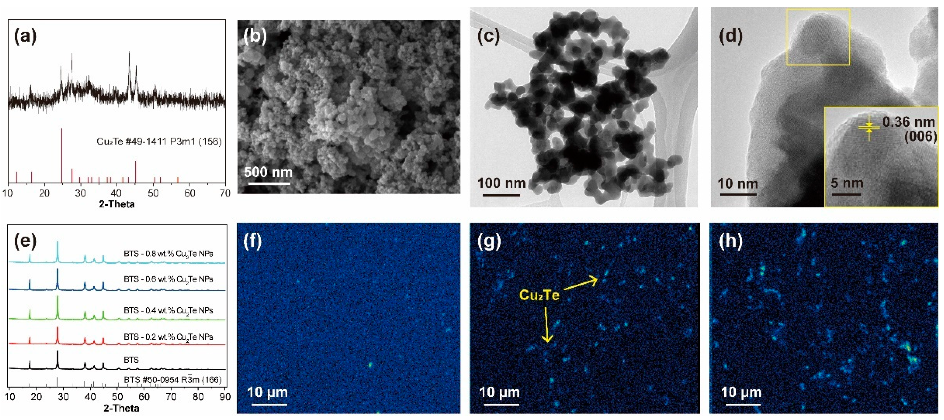
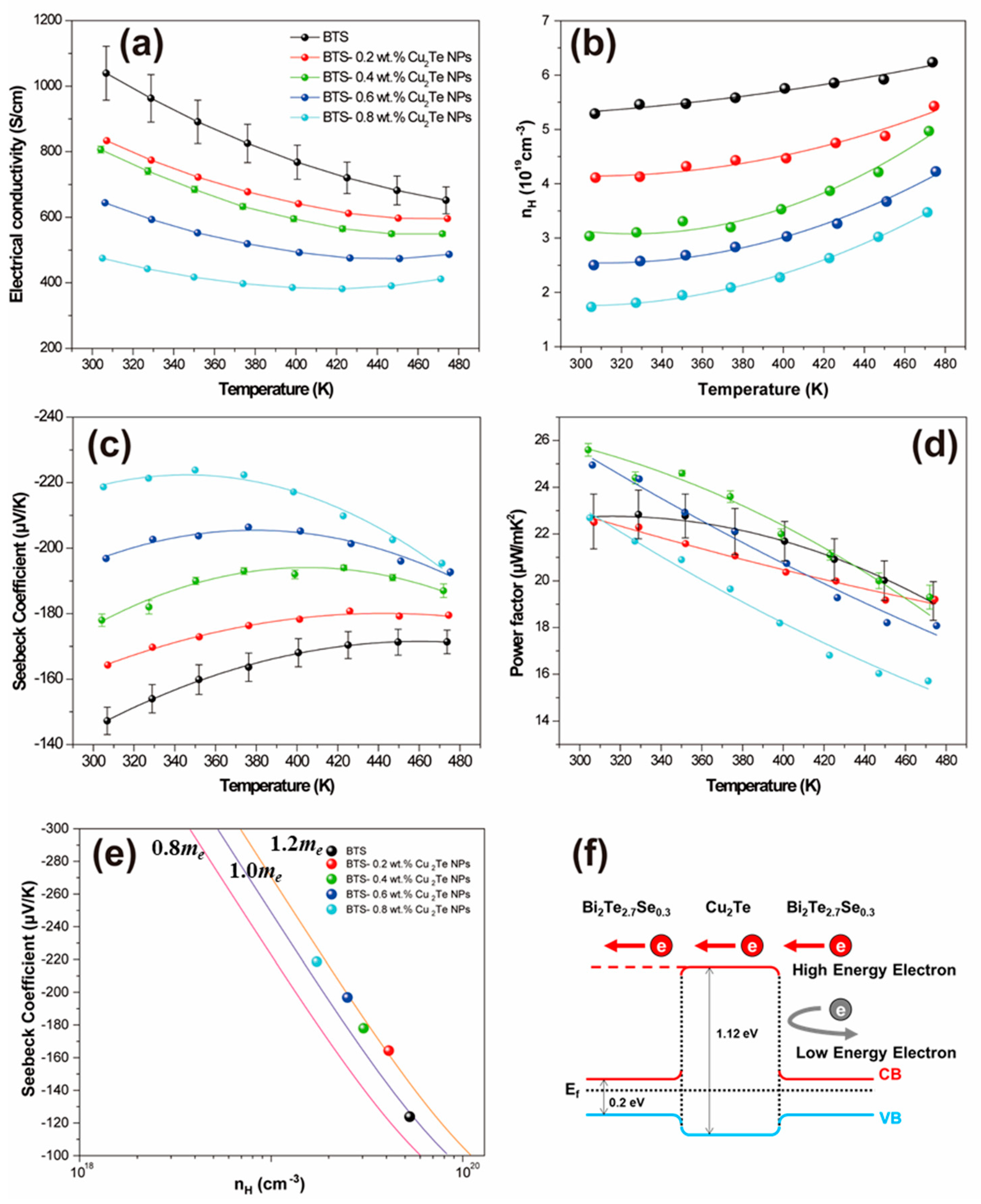
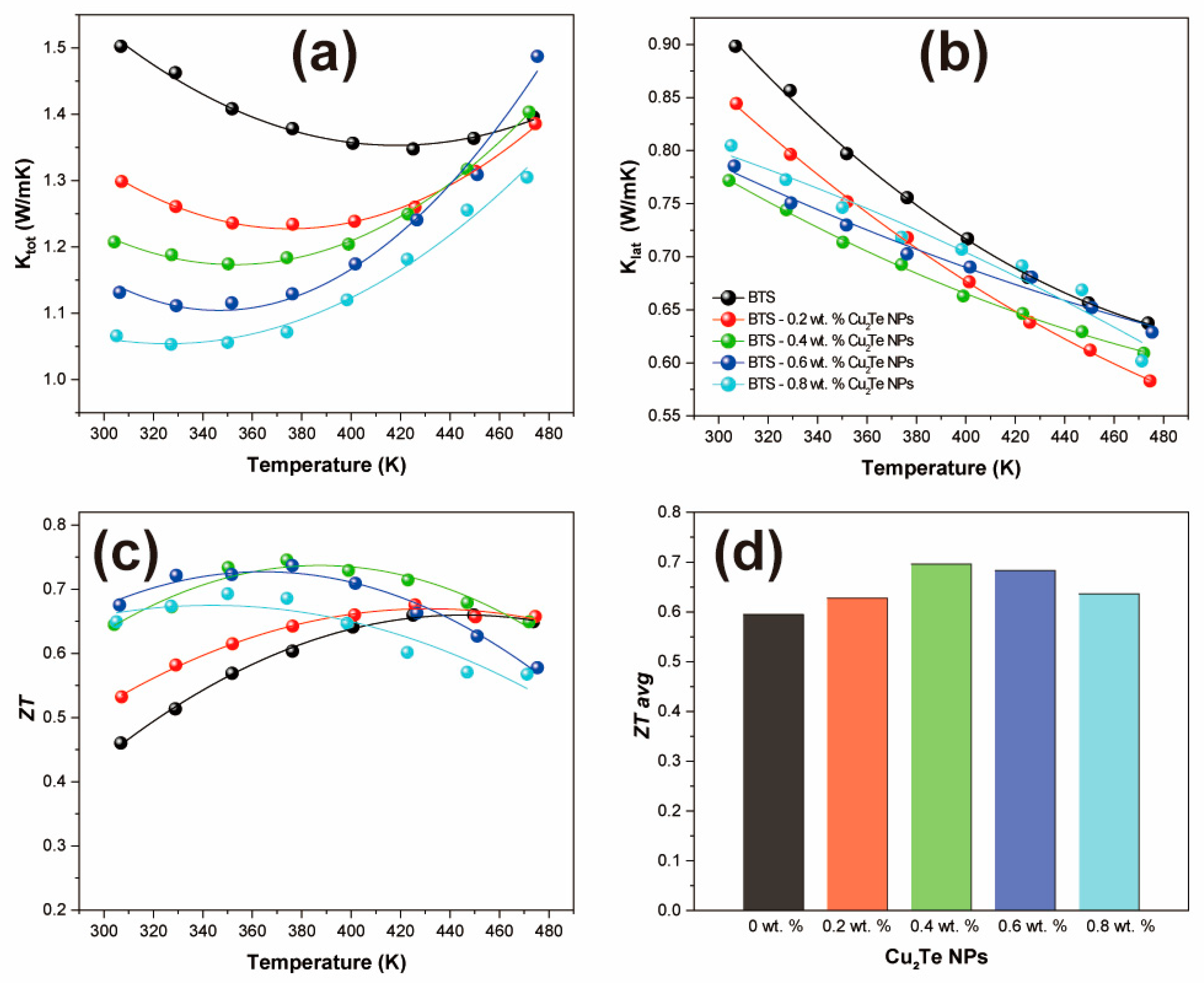
3. Results and Discussions

Figure 1a shows the XRD pattern of as-prepared Cu2Te NPs obtained by the chemical reduction method. Our Cu2Te NPs has a hexagonal structure with the space group of P3m1 (JCPDS # 49-1441). The XRD peaks are not strong due to the small size of Cu2Te NPs. The size of as-prepared Cu2Te is 20–50 nm from the SEM and TEM images (Figure 1b,c), and the high resolution TEM image shows the lattice distance of 0.36 nm, which corresponds to (006) plane of Cu2Te phase. Figure 1e presents the powder XRD patterns of the BTS-x wt.% Cu2Te NP (x = 0, 0.2, 0.4, 0.6, and 0.8) composite materials. All samples show typical BTS patterns (rhombohedral structure, space group of R-3m, JCPDS # 50-0594) without any additional peaks. The lattice parameters of the BTS-x wt.% Cu2Te NP (x = 0, 0.2, 0.4, 0.6, and 0.8) are summarized in Table 1, and there are no significant changes in lattice parameters by Cu2Te NPs incorporation. The small size and low content of Cu2Te NPs in the composite powder were not detectable by XRD (Figure 1e). We analysed the Cu2Te nanophases on BTS-x wt.% Cu2Te NP (x = 0.2, 0.4, and 0.6) bulk samples by EPMA (Figure 1f–h), where the light parts of the Cu mapping were matched with the Cu2Te nanophases. Cu2Te NPs can be easily observed on the parent bulk materials, and as the amount of Cu2Te NPs increases, a homogeneous distribution of Cu2Te NPs can be found. However, for the BTS-0.6 wt.% Cu2Te NPs sample, some Cu2Te NPs exhibit agglomeration, which means that a large amount (more than 0.6 wt.%) of Cu2Te NPs on BTS cannot be dispersed uniformly.
Figure 2a presents the temperature dependence of the electrical conductivity (σ) for BTS-x wt.% Cu2Te NPs (x = 0, 0.2, 0.4, 0.6, and 0.8). The electrical conductivity gradually decreases over the entire temperature range studied here as the Cu2Te NP incorporation increases. The electrical conductivities of BTS-x wt.% Cu2Te NPs (x = 0, 0.2, 0.4, and 0.6) decrease with increasing temperature, indicating semi-metallic or metallic conduction behaviour. However, the sample with a high amount of Cu2Te NPs (0.8 wt.%) incorporated shows semiconducting behaviour at a high temperature due to the carrier concentration decrease shown in Figure 2b. The carrier concentration obtained from the Hall measurements decreases as the amount of Cu2Te NPs increases. The Cu intercalation in the van der Waals gap between Te–Te shows donor-like behaviour, while our Cu2Te incorporation shows acceptor-like behaviour. The temperature dependence of the Seebeck coefficient (S) for the BTS-x wt.% Cu2Te NP (x = 0, 0.2, 0.4, 0.6, and 0.8) samples is displayed in Figure 2c. All samples exhibit negative S values, indicating that electrons constitute the majority of the charge carriers, which is consistent with the signs of the respective Hall measurements. The temperature at which the S peaks (Tmax) are shifted to lower temperatures with increasing Cu2Te incorporation, and the absolute value of S maximum (Smax) increases as the amount of incorporated Cu2Te increases. Typically, BTS show anisotropic nature of TE properties due to Te vacancies and antisite defects [24]. It is noted that the reproducibility (collecting the results for more than 5 different batches) of electrical properties is greatly enhanced through Cu2Te introduction.
Usually, the Tmax shift to lower temperatures originates from increased bipolar conduction, but the corresponding Smax should also be decreased. Improvement of the bipolar conduction cannot explain the observed increase in Smax with increasing Cu2Te. From Pisarenko’s relation [1,25], one can estimate the density of states (DOS) effective mass with the assumption of a single parabolic band model using the following Equation (1):
S = 8 π 2 k B 2 3 e h 2 ( π 3 n ) 2 / 3 m d * T
where h is the Planck constant, kB is the Boltzmann constant, m d * is the DOS effective mass, e is the electronic charge, and n is the carrier concentration. As shown in Figure 2e, the pristine BTS has an m d * value of 0.97 me (me is the electron rest mass), whereas Cu2Te NP incorporation increases the m d * value of 1.16 me in the BTS-0.4 wt.% Cu2Te NP sample at room temperature. Therefore, the increase in m d * with Cu2Te incorporation can enhance Smax, even when the bipolar conduction becomes strong. The n reduction observed with the incorporation of Cu2Te is also responsible for the increase in Smax. The m d * change could be attributed to the engineered band structure interface between the BTS matrix and Cu2Te NPs. In this context, we can suggest a band diagram that describes the interfacial band bending between the BTS and Cu2Te NPs (Figure 2f). The electron energy barrier, i.e., the hetero-interface of the conduction bands between the BTS and Cu2Te NPs, filters the low-energy carriers. The electron affinity and band gap of BTS and Cu2Te were obtained from the literature [26,27,28,29]. A previous theoretical study of PbTe TE materials showed that ~1.5 nm nanoinclusion significantly enhanced the S value [15]. The electrostatic potential only affected the interface between the nanoinclusion and the matrix, and larger nanoinclusions were less effective than smaller nanoinclusions. Our synthesized Cu2Te NPs had sizes of ~50 nm, so we expected that the smaller Cu2Te NPs could have a greater effect. The BTS-0.4 wt.% Cu2Te NP sample has the highest calculated power factor (S2σ), which is ~15% higher at room temperature than that of the pristine BTS sample.
The temperature dependence of the total thermal conductivity (κtot) of BTS-x wt.% Cu2Te NPs (x = 0, 0.2, 0.4, 0.6, and 0.8) is shown in Figure 3a. All samples display very low κtot values over the entire temperature range studied here and also exhibit upturns. The occurrence temperatures of the upturns in the thermal conductivity data move to lower temperatures with increasing Cu2Te incorporation amounts, which is consistent with the behaviour of S and σ. This increase in thermal conductivity is due to the bipolar diffusion of the carriers and is still present in the BTS sample at elevated temperatures, as shown in Figure 3a. This increase in κtot with temperature is attributable to the thermal energy transported by electron–hole pairs, which is equal to the energy of the gap between the hot and cold sides of the sample. This bipolar diffusion phenomenon results in an increase in the heat transfer beyond what is expected from the normal carrier contribution (κele) to κ defined by the Wiedemann-Franz law [30], κele = LσT, where L is the Lorenz number. The Lorenz number is estimated by assuming a single parabolic band and acoustic phonon scattering using the following Equations (2)–(4):
S = ± k B e [ ( r + 5 / 2 ) F r + 3 / 2 ( ξ ) ( r + 3 / 2 ) F r + 1 / 2 ( ξ ) ξ ]
F n ( ξ ) = 0 x n 1 + e ( x ξ ) d x
L = ( k B e ) 2 [ ( r + 7 / 2 ) F r + 5 / 2 ( ξ ) ( r + 3 / 2 ) F r + 1 / 2 ( ξ ) ( ( r + 5 / 2 ) F r + 3 / 2 ( ξ ) ( r + 3 / 2 ) F r + 1 / 2 ( ξ ) ) 2 ]
Here, ξ, Fn(ξ), and r are the reduced Fermi energy ((EvEF)/kBT), Fermi integral of order n, and scattering parameter, respectively. We set r = 0–1/2 for acoustic phonon scattering. The temperature dependence of the lattice thermal conductivity (κlat) can be estimated by deducting the bipolar conduction portion (κbp) and electronic portion (κele) of thermal transport from the total thermal conductivity; κlat = κtotκbpκele. κbp was calculated using the below Equation (5).
κ b p = ( i S i 2 σ i S 2 σ ) T .
Si, σi, S, and σ are the Seebeck coefficient and electrical conductivity of an individual band, total Seebeck coefficient, and electrical conductivity from both the conduction and valence bands, respectively. S and σ are in turn defined as follows Equations (6) and (7):
σ = i σ i
S = i S i σ i i σ i
Using the two-band (TB) model (an extension of the single parabolic band model), which includes one valence band and one conduction band, band parameters such as the density-of-states effective mass ( m d * ) and non-degenerate mobility (μ0) of each band were obtained. Specifically, the m d * and μ0 of individual band were estimated by fitting the TB model to Hall carrier concentration (nH)-dependent S and nH-dependent σ measurements, respectively [31]. The band gap between the valence and conduction bands required in the TB model was adopted from the literature [32]. Once m d , i * and μ0,i (i = valence and conduction bands) were estimated, corresponding Si and σi (i = valence and conduction bands) were calculated. Furthermore, theoretical total S and σ (which agree well with experimental S and σ) were computed with Si and σi according to Equations (6) and (7). Finally, the calculated Si, σi, S, and σ were substituted back into Equation (5) to estimate κbp.
The incorporation of Cu2Te NPs encourages bipolar conduction and, consequently, κlat (shown in Figure 3b), after Cu2Te NP incorporation is reduced over the entire temperature range due to enhanced phonon scattering. The reduction in κlat occurs up to 0.4 wt.% Cu2Te NPs incorporation, whereas more Cu2Te NPs produce a negative phonon scattering effect by agglomeration of Cu2Te NPs. Generally, it is acceptable that the introduction of secondary phases decreases κlat by phonon scattering. However, the size of the secondary phase is an important factor for enhancing phonon scattering. Particles with sizes larger than hundreds of nanometres have a limited effect on κlat [33]. Our κlat results after Cu2Te agglomeration (more than 0.6 wt.% Cu2Te NPs) could be described similarly. The size of the Cu2Te NPs was ~50 nm, and if several Cu2Te NPs were agglomerated, the size was easily greater than a hundred nanometres. In addition, the previous report also shows that reduced particle size with the same volume fraction could decrease thermal conductivity more [34]. Therefore, a homogeneous dispersion of small Cu2Te NPs is necessary for encouraging phonon scattering and enhancing the electrical properties.
Collecting the above effects, ZT is shown as a function of temperature for BTS-x wt.% Cu2Te NPs (x = 0, 0.2, 0.4, 0.6, and 0.8) in Figure 3c. The highest ZT of 0.75 is observed at 374 K for the BTS-0.4 wt.% Cu2Te NPs sample, which is 15% higher than that of the pristine sample. It is noteworthy that the maximum ZT temperature for each sample is modulated by the introduction of Cu2Te NPs, decreasing as the amount of Cu2Te NPs increases. The simple incorporation of Cu2Te can easily modulate the temperature dependence of n-type TE materials, and we suggest that the TE properties can be precisely controlled according to the target application, such as cooling or low-temperature energy harvesting. The average ZT value (ZTavg) in the temperature range studied here is shown in Figure 3d. ZTavg reaches 0.70 for the BTS-0.4 wt.% Cu2Te NPs sample, representing 19% enhancement compared to the pristine BTS matrix.

4. Conclusions

In conclusion, we investigated the TE properties of n-type BTS by incorporating Cu2Te NPs. The incorporation of Cu2Te NPs encourages the Seebeck coefficient and power factor, and we thought that the band bending between the interface of the BTS and Cu2Te NPs could filter the low-energy electron carrier. The Cu2Te NPs on the BTS matrix also affect κlat by encouraging phonon scattering. Together with modulating the electrical and thermal properties, the maximum ZT value reaches 0.75 at 374 K for the BTS-0.4 wt.% Cu2Te NPs sample, 15% higher than that of pristine BTS (0.65 at 425 K). In addition, the temperature dependence of ZT can be controlled by the Cu2Te NP dispersion just before the sintering process, which is a great advantage for target applications. Further advances could be expected by developing the synthesis of Cu2Te NPs with sizes of several nanometres.

Author Contributions

Conceptualization, W.H.S. and J.Y.C.; methodology, Y.-J.J., E.Y.J. and H.-S.K.; validation, W.H.N., N.V.B. and M.K. (Minji Kang); investigation, J.H.W., M.K. (Minkyung Kim), S.-M.K., S.-i.K. and H.-S.K.; data curation, Y.-J.J., J.-M.O. and W.H.S.; writing—original draft preparation, Y.-J.J., H.-S.K. and J.W.R.; writing—review and editing, J.Y.C. and W.H.S.; visualization, Y.-J.J. and K.-S.M.; funding acquisition, S.-M.K. and W.H.S. All authors have read and agreed to the published version of the manuscript.

Funding

This work was grant funded by the Korea Government (MOTIE) (P0012451, The Competency Development Program for Industry Specialist), Technology Development Program (S3033211) funded by the Ministry of SMEs and Startups (MSS, Korea), and Korea Institute of Ceramic Engineering and Technology (KPP19001). The present research has been also conducted by the Research Grant of Kwangwoon University in 2021.

Institutional Review Board Statement

Not applicable.

Informed Consent Statement

Not applicable.

Data Availability Statement

The data presented in this study are available upon request from the corresponding author.

Conflicts of Interest

The authors declare no conflict of interest.

References

  1. Snyder, G.J.; Toberer, E.S. Complex thermoelectric materials. Nat. Mater. 2008, 7, 105–114. [Google Scholar] [CrossRef] [PubMed]
  2. Shi, X.-L.; Zou, J.; Chen, Z.-G. Advanced thermoelectric design: From materials and structures to devices. Chem. Rev. 2020, 120, 7399–7515. [Google Scholar] [CrossRef] [PubMed]
  3. Funahashi, R.; Barbier, T.; Combe, E. Thermoelectric materials for middle and high temperature ranges. J. Mater. Res. 2015, 30, 2544–2557. [Google Scholar] [CrossRef]
  4. Shi, X.; Yang, J.; Wu, L.; Salvador, J.R.; Zhang, C.; Villaire, W.L.; Haddad, D.; Yang, J.; Zhu, Y.; Li, Q. Band structure engineering and thermoelectric properties of charge-compensated filled skutterudites. Sci. Rep. 2015, 5, 14641. [Google Scholar] [CrossRef] [PubMed] [Green Version]
  5. Pei, Y.; Tan, G.; Feng, D.; Zheng, L.; Tan, Q.; Xie, X.; Gong, S.; Chen, Y.; Li, J.F.; He, J. Integrating band structure engineering with all-scale hierarchical structuring for high thermoelectric performance in PbTe system. Adv. Energy Mater. 2017, 7, 1601450. [Google Scholar] [CrossRef]
  6. Yoon, J.S.; Song, J.M.; Rahman, J.U.; Lee, S.; Seo, W.S.; Lee, K.H.; Kim, S.; Kim, H.-S.; Kim, S.-I.; Shin, W.H. High thermoelectric performance of melt-spun CuxBi0.5Sb1.5Te3 by synergetic effect of carrier tuning and phonon engineering. Acta Mater. 2018, 158, 289–296. [Google Scholar] [CrossRef]
  7. Jood, P.; Male, J.P.; Anand, S.; Matsushita, Y.; Takagiwa, Y.; Kanatzidis, M.G.; Snyder, G.J.; Ohta, M. Na doping in PbTe: Solubility, band convergence, phase boundary mapping, and thermoelectric properties. J. Am. Chem. Soc. 2020, 142, 15464–15475. [Google Scholar] [CrossRef] [PubMed]
  8. Poudel, B.; Hao, Q.; Ma, Y.; Lan, Y.; Minnich, A.; Yu, B.; Yan, X.; Wang, D.; Muto, A.; Vashaee, D. High-thermoelectric performance of nanostructured bismuth antimony telluride bulk alloys. Science 2008, 320, 634–638. [Google Scholar] [CrossRef] [PubMed] [Green Version]
  9. Cai, X.; Rong, Z.; Yang, F.; Gan, Z.; Li, G. Improved thermoelectric properties of Bi2Te3−xSex alloys by melt spinning and resistance pressing sintering. J. Phys. D Appl. Phys. 2014, 47, 115101. [Google Scholar] [CrossRef]
  10. Ahn, K.; Biswas, K.; He, J.; Chung, I.; Dravid, V.; Kanatzidis, M.G. Enhanced thermoelectric properties of p-type nanostructured PbTe–MTe (M = Cd, Hg) materials. Energy Environ. Sci. 2013, 6, 1529–1537. [Google Scholar] [CrossRef]
  11. Shin, W.H.; Roh, J.W.; Ryu, B.; Chang, H.J.; Kim, H.S.; Lee, S.; Seo, W.S.; Ahn, K. Enhancing thermoelectric performances of bismuth antimony telluride via synergistic combination of multiscale structuring and band alignment by FeTe2 incorporation. ACS Appl. Mater. Interfaces 2018, 10, 3689–3698. [Google Scholar] [CrossRef]
  12. Kim, S.I.; Lee, K.H.; Mun, H.A.; Kim, H.S.; Hwang, S.W.; Roh, J.W.; Yang, D.J.; Shin, W.H.; Li, X.S.; Lee, Y.H. Dense dislocation arrays embedded in grain boundaries for high-performance bulk thermoelectrics. Science 2015, 348, 109–114. [Google Scholar] [CrossRef] [PubMed] [Green Version]
  13. Koh, Y.K.; Vineis, C.; Calawa, S.; Walsh, M.; Cahill, D.G. Lattice thermal conductivity of nanostructured thermoelectric materials based on PbTe. Appl. Phys. Lett. 2009, 94, 153101. [Google Scholar] [CrossRef]
  14. Wu, H.; Carrete, J.; Zhang, Z.; Qu, Y.; Shen, X.; Wang, Z.; Zhao, L.-D.; He, J. Strong enhancement of phonon scattering through nanoscale grains in lead sulfide thermoelectrics. NPG Asia Mater. 2014, 6, e108. [Google Scholar] [CrossRef]
  15. Faleev, S.V.; Léonard, F. Theory of enhancement of thermoelectric properties of materials with nanoinclusions. Phys. Rev. B 2008, 77, 214304. [Google Scholar] [CrossRef] [Green Version]
  16. Li, Y.; Qin, X.; Li, D.; Zhang, J.; Li, C.; Liu, Y.; Song, C.; Xin, H.; Guo, H. Enhanced thermoelectric performance of Cu2Se/Bi0.4Sb1.6Te3 nanocomposites at elevated temperatures. Appl. Phys. Lett. 2016, 108, 062104. [Google Scholar] [CrossRef]
  17. Cho, H.; Back, S.Y.; Yun, J.H.; Byeon, S.; Jin, H.; Rhyee, J.-S. Thermoelectric properties and low-energy carrier filtering by Mo microparticle dispersion in an n-type (CuI)0.003Bi2(Te, Se)3 bulk matrix. ACS Appl. Mater. Interfaces 2020, 12, 38076–38084. [Google Scholar] [CrossRef]
  18. Tan, G.; Shi, F.; Hao, S.; Zhao, L.-D.; Chi, H.; Zhang, X.; Uher, C.; Wolverton, C.; Dravid, V.P.; Kanatzidis, M.G. Non-equilibrium processing leads to record high thermoelectric figure of merit in PbTe–SrTe. Nat. Commun. 2016, 7, 12167. [Google Scholar] [CrossRef]
  19. Kim, S.I.; Hwang, S.; Roh, J.W.; Ahn, K.; Yeon, D.-H.; Lee, K.H.; Kim, S.W. Experimental evidence of enhancement of thermoelectric properties in tellurium nanoparticle-embedded bismuth antimony telluride. J. Mater. Res. 2012, 27, 2449–2456. [Google Scholar] [CrossRef]
  20. Li, S.; Liu, X.; Liu, Y.; Liu, F.; Luo, J.; Pan, F. Optimized hetero-interfaces by tuning 2D SnS2 thickness in Bi2Te2.7Se0.3/SnS2 nanocomposites to enhance thermoelectric performance. Nano Energy 2017, 39, 297–305. [Google Scholar] [CrossRef]
  21. Wu, H.-J.; Yen, W.-T. High thermoelectric performance in Cu-doped Bi2Te3 with carrier-type transition. Acta Mater. 2018, 157, 33–41. [Google Scholar] [CrossRef]
  22. Lognoné, Q.; Gascoin, F. Reactivity, stability and thermoelectric properties of n-Bi2Te3 doped with different copper amounts. J. Alloys Compd. 2014, 610, 1–5. [Google Scholar] [CrossRef]
  23. Han, M.-K.; Jin, Y.; Lee, D.-H.; Kim, S.-J. Thermoelectric properties of Bi2Te3: CuI and the effect of its doping with Pb atoms. Materials 2017, 10, 1235. [Google Scholar] [CrossRef] [PubMed] [Green Version]
  24. Liu, W.S.; Zhang, Q.; Lan, Y.; Chen, S.; Yan, X.; Zhang, Q.; Wang, H.; Wang, D.; Chen, G.; Ren, Z. Thermoelectric property studies on Cu-doped n-type CuxBi2Te2.7Se0.3 nanocomposites. Adv. Energy Mater. 2011, 1, 577–587. [Google Scholar] [CrossRef]
  25. Ioffe, A.F. Physics of Semiconductors; Academic Press: Cambridge, MA, USA, 1960. [Google Scholar]
  26. Rahman, M.W.; Rahman, S.I.; Ahmed, S.N.; Hoque, M.A. Numerical Analysis of CdS: O/CdTe Thin Film Solar Cell using Cu2Te BSF Layer. In Proceedings of the 9th International Conference on Electrical and Computer Engineering (ICECE), Dhaka, Bangladesh, 20–22 December 2016; IEEE: Piscataway, NJ, USA, 2016; pp. 279–282. [Google Scholar]
  27. Li, F.; Zhai, R.; Wu, Y.; Xu, Z.; Zhao, X.; Zhu, T. Enhanced thermoelectric performance of n-type bismuth-telluride-based alloys via In alloying and hot deformation for mid-temperature power generation. J. Mater. 2018, 4, 208–214. [Google Scholar] [CrossRef]
  28. Sun, T.; Samani, M.K.; Khosravian, N.; Ang, K.M.; Yan, Q.; Tay, B.K.; Hng, H.H. Enhanced thermoelectric properties of n-type Bi2Te2.7Se0.3 thin films through the introduction of Pt nanoinclusions by pulsed laser deposition. Nano Energy 2014, 8, 223–230. [Google Scholar] [CrossRef]
  29. Zhang, Y.; Wang, Y.; Xi, L.; Qiu, R.; Shi, X.; Zhang, P.; Zhang, W. Electronic structure of antifluorite Cu2X (X = S, Se, Te) within the modified Becke-Johnson potential plus an on-site Coulomb U. J. Chem. Phys. 2014, 140, 074702. [Google Scholar] [CrossRef] [PubMed]
  30. Kittel, C. Introduction to Solid State Physics, 6th ed.; John Wiley & Sons. Inc.: New York, NY, USA, 2005. [Google Scholar]
  31. Kim, M.; Kim, S.I.; Kim, S.W.; Kim, H.S.; Lee, K.H. Weighted Mobility Ratio Engineering for High-Performance Bi-Te-Based Thermoelectric Materials via Suppression of Minority Carrier Transport. Adv. Mater. 2021, 33, 2005931. [Google Scholar] [CrossRef] [PubMed]
  32. Witting, I.T.; Chasapis, T.C.; Ricci, F.; Peters, M.; Heinz, N.A.; Hautier, G.; Snyder, G.J. The thermoelectric properties of bismuth telluride. Adv. Electron. Mater. 2019, 5, 1800904. [Google Scholar] [CrossRef]
  33. Lee, K.H.; Kim, Y.-M.; Park, C.O.; Shin, W.H.; Kim, S.W.; Kim, H.-S.; Kim, S.-I. Cumulative Defect Structures for Experimentally-Attainable Low Thermal Conductivity in Thermoelectric (Bi, Sb)2Te3 Alloys. Mater. Today Energy 2021, 21, 100795. [Google Scholar] [CrossRef]
  34. Parasuraman, R.; Wu, Y.; Ordonez-Miranda, J.; Volz, S.; Umarji, A.M. Particle size effect on the thermal conductivity reduction of silicon based thermoelectric composites. Sustain. Energy Fuels 2018, 2, 1764–1771. [Google Scholar] [CrossRef]
Figure 1. (a) XRD pattern, (b) SEM image, (c) TEM image, and (d) high resolution TEM image of Cu2Te NPs, (e) XRD patterns of BTS-x wt.% Cu2Te NPs (x = 0, 0.2, 0.4, 0.6, and 0.8), Cu K mapping images of EPMA for (f) BTS-0.2 wt.% Cu2Te NPs, (g) BTS-0.4 wt.% Cu2Te NPs, and (h) BTS-0.6 wt.% Cu2Te NPs, where the light dots correspond to elemental Cu.
Materials 15 02284 g001
Figure 2. Electrical properties of BTS-x wt.% Cu2Te NPs (x = 0, 0.2, 0.4, 0.6, and 0.8). (a) Electrical conductivities, (b) electron carrier concentrations obtained by Hall measurement, (c) Seebeck coefficients, (d) power factors, (e) Pisarenko’s plot, and (f) band diagram of BTS and Cu2Te NPs interfaces.
Materials 15 02284 g002
Figure 3. (a) Total thermal conductivities, (b) lattice thermal conductivities, (c) ZT values, and (d) average ZT values between room temperature and 470 K of BTS-x wt.% Cu2Te NPs (x = 0, 0.2, 0.4, 0.6, and 0.8).
Materials 15 02284 g003
Table 1. The lattice parameters of BTS-x wt.% Cu2Te NPs (x = 0, 0.2, 0.4, 0.6, and 0.8).
Lattice Constant for a (Å)Lattice Constant for c (Å)
BTS4.361930.3632
BTS-0.2 wt.% Cu2Te NPs4.361430.3604
BTS-0.4 wt.% Cu2Te NPs4.361530.3641
BTS-0.6 wt.% Cu2Te NPs4.361030.3606
BTS-0.8 wt.% Cu2Te NPs4.361430.3650
Publisher’s Note: MDPI stays neutral with regard to jurisdictional claims in published maps and institutional affiliations.

