
Computation of the Electrical Resistance of a Low Current Multi-Spot Contact


Abstract
:1. Introduction
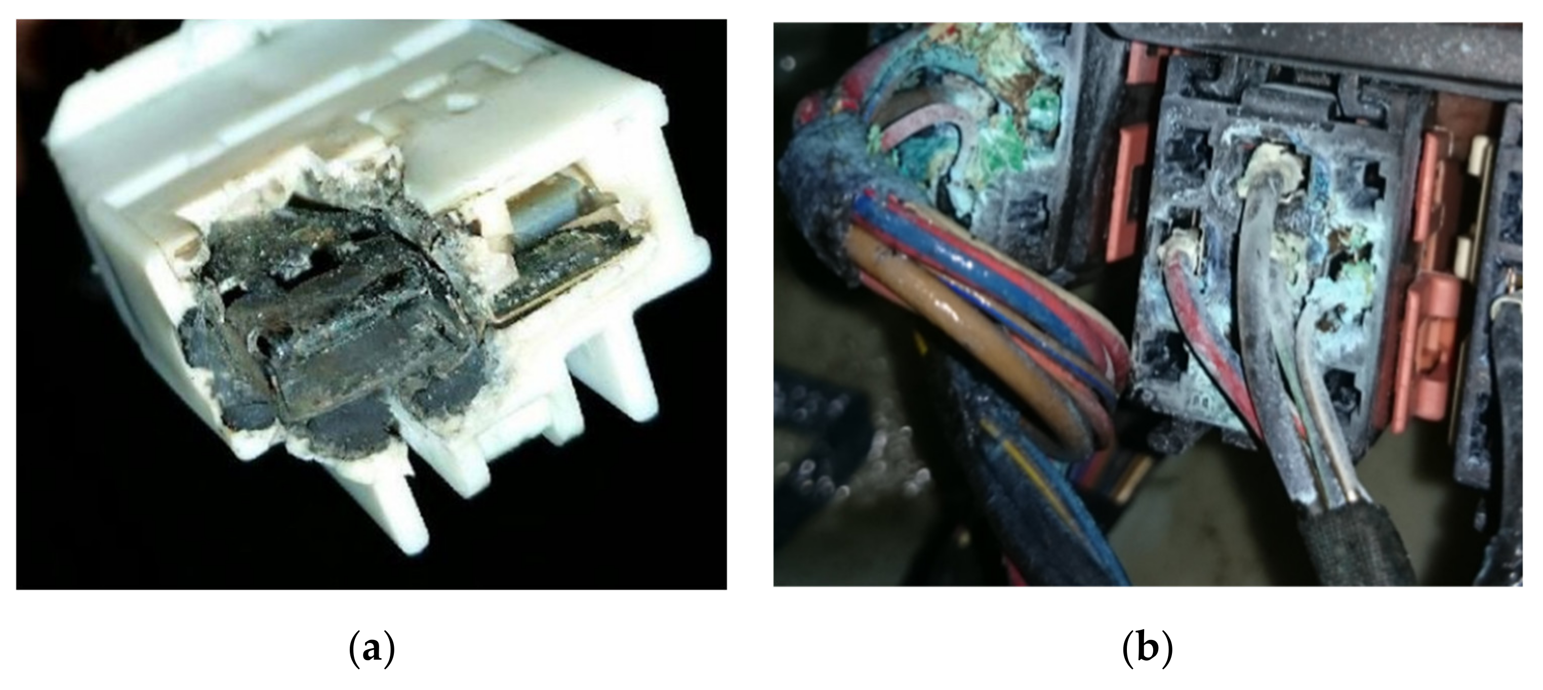
Aging of Electrical Contacts
2. Analytical Models for Contact Resistance
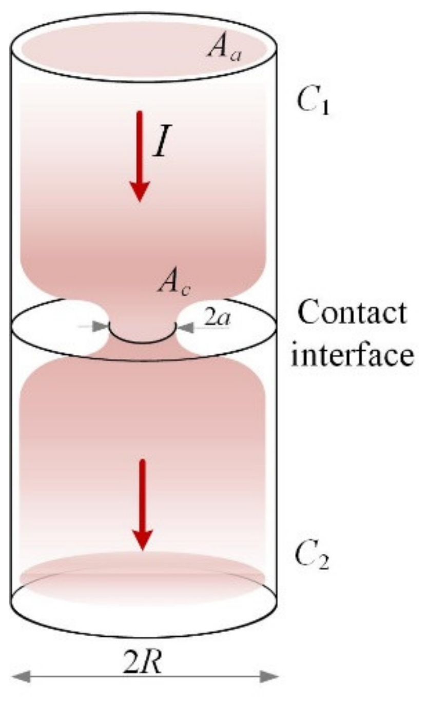
2.1. Holm’s Analytical Model for Contact Resistance
- No presence of oxide films or impurities at the interface of the metallic cylinders;
- There is no axial deviation in the direction of current flow;
- The metallic cylinders in contact have infinite dimensions to the current flow.
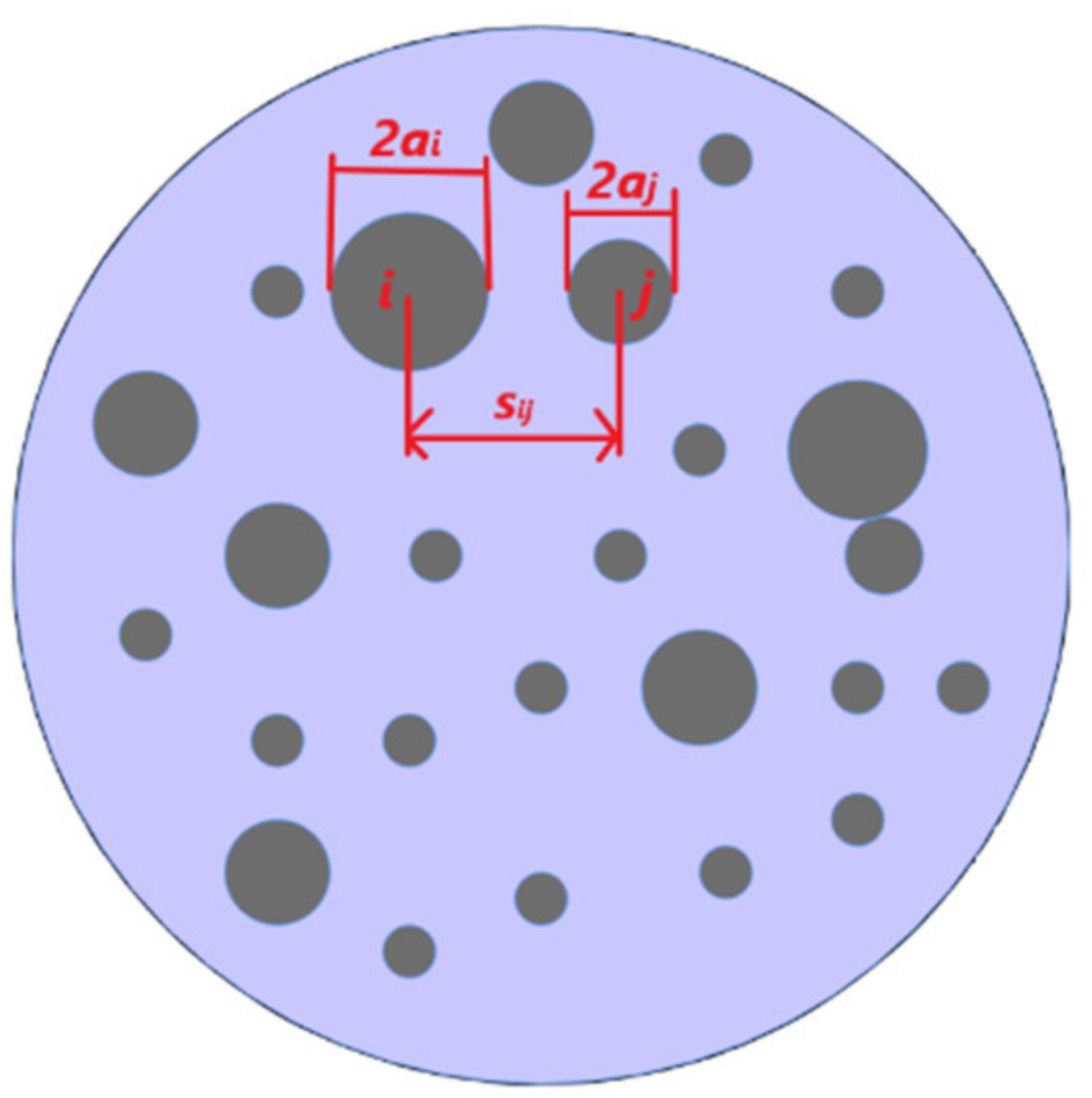
2.2. Greenwood’s Analytical Model for Contact Resistance
3. Numerical Model
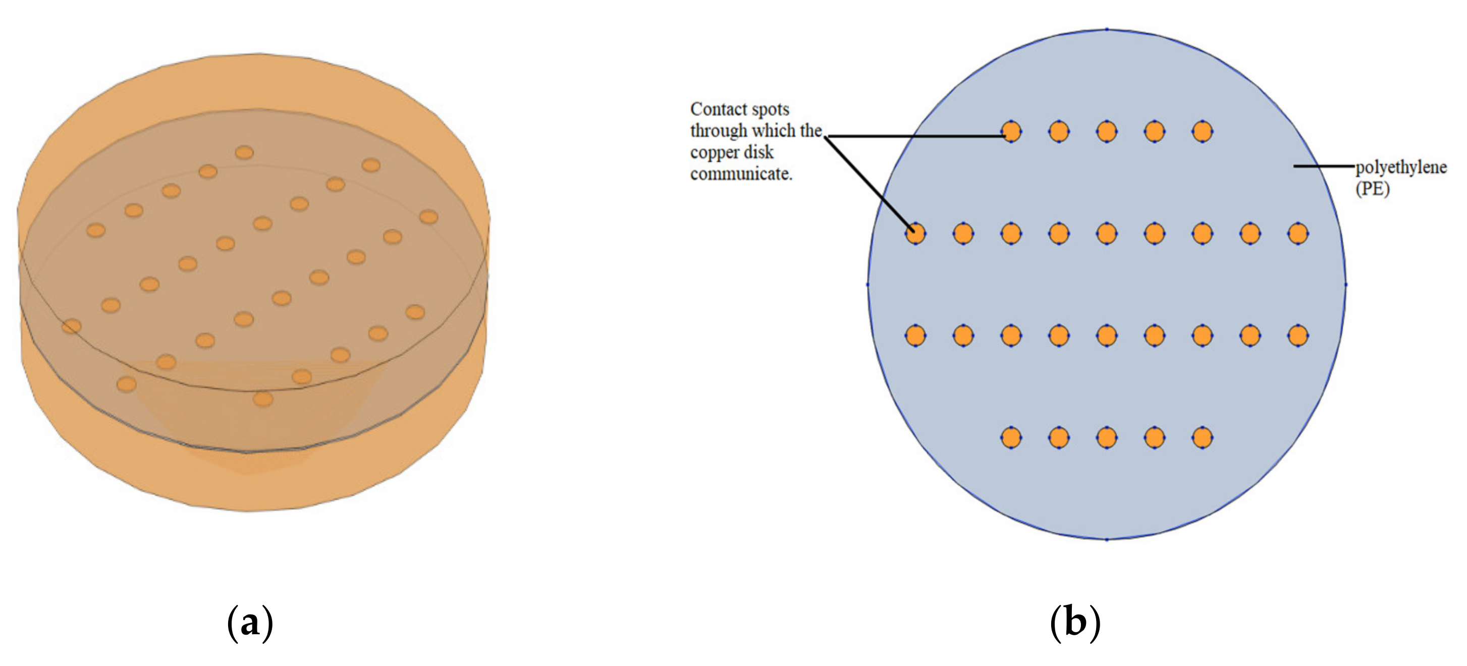
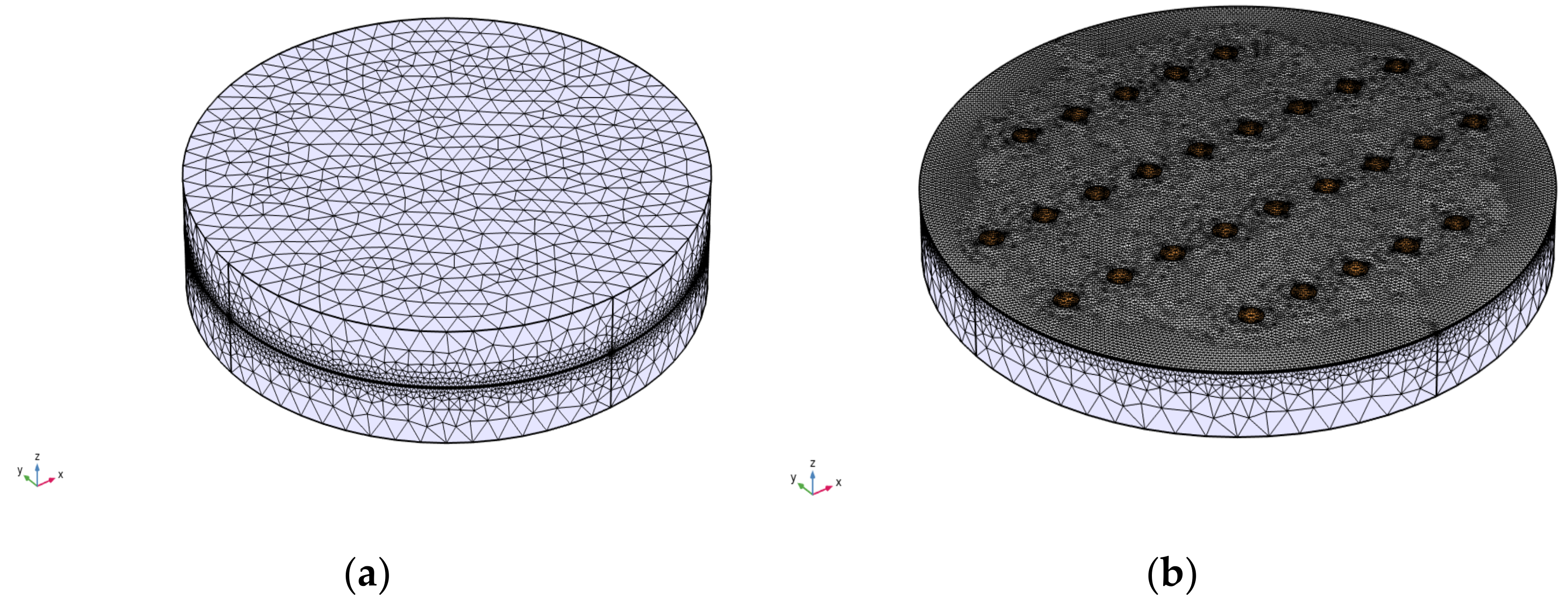
3.1. Geometrical Model
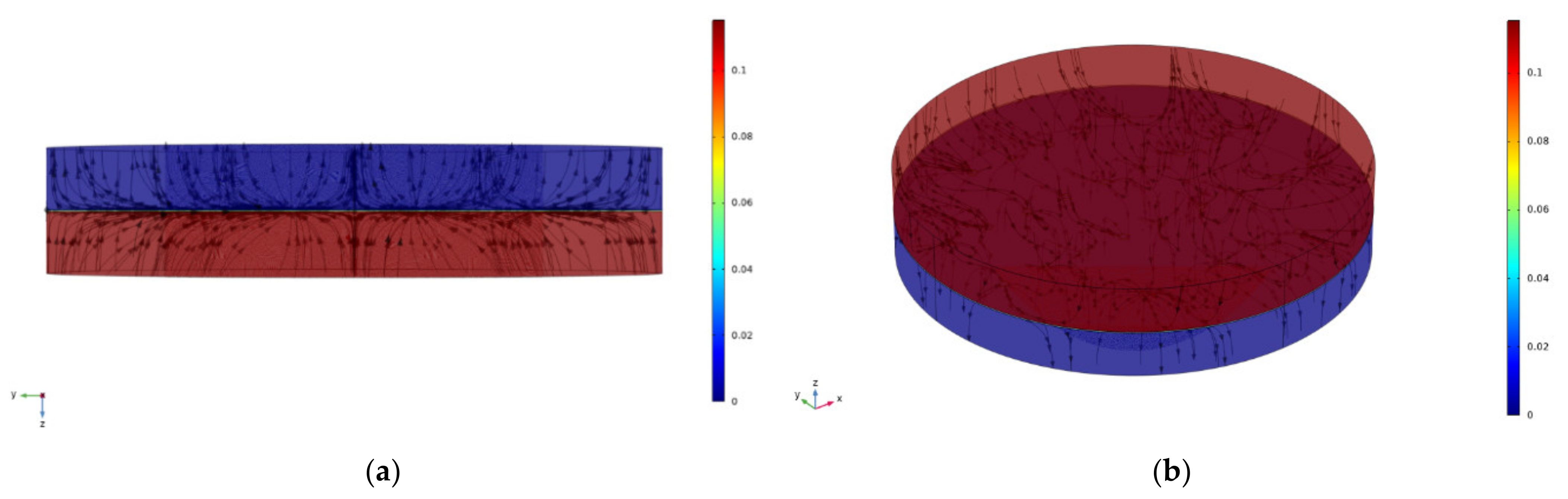
3.2. Mathematical Model
Boundary Conditions
- Continuity (9): this signifies that the normal components of the injected current flowing through the copper disks are continuous and conserved across the interior boundaries of both disks:n∙(J1 − J2) = 0
- Insulation (10): this specifies that no current flows across the boundary. It applies to all surfaces except the contact areas:n∙J = 0
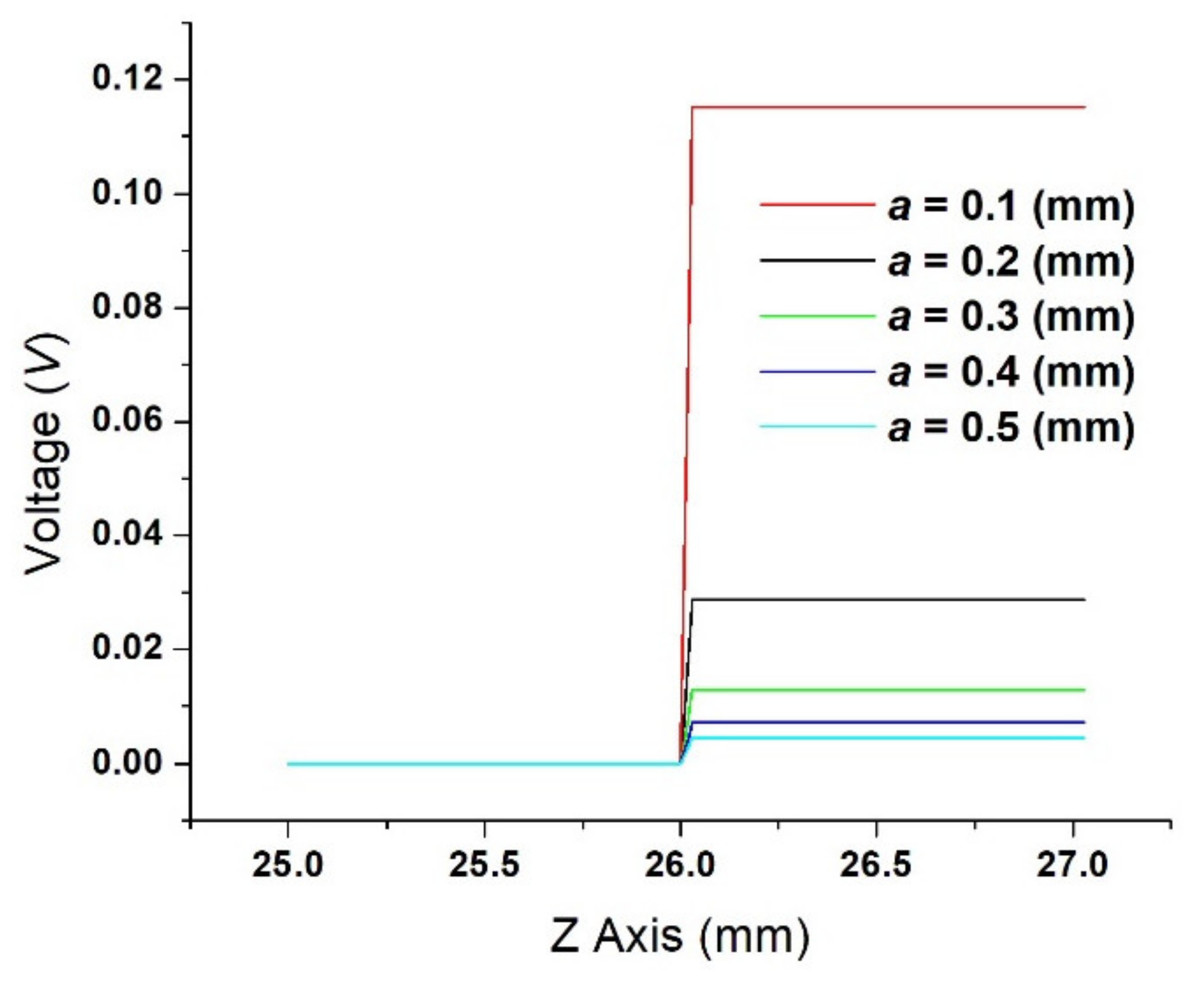
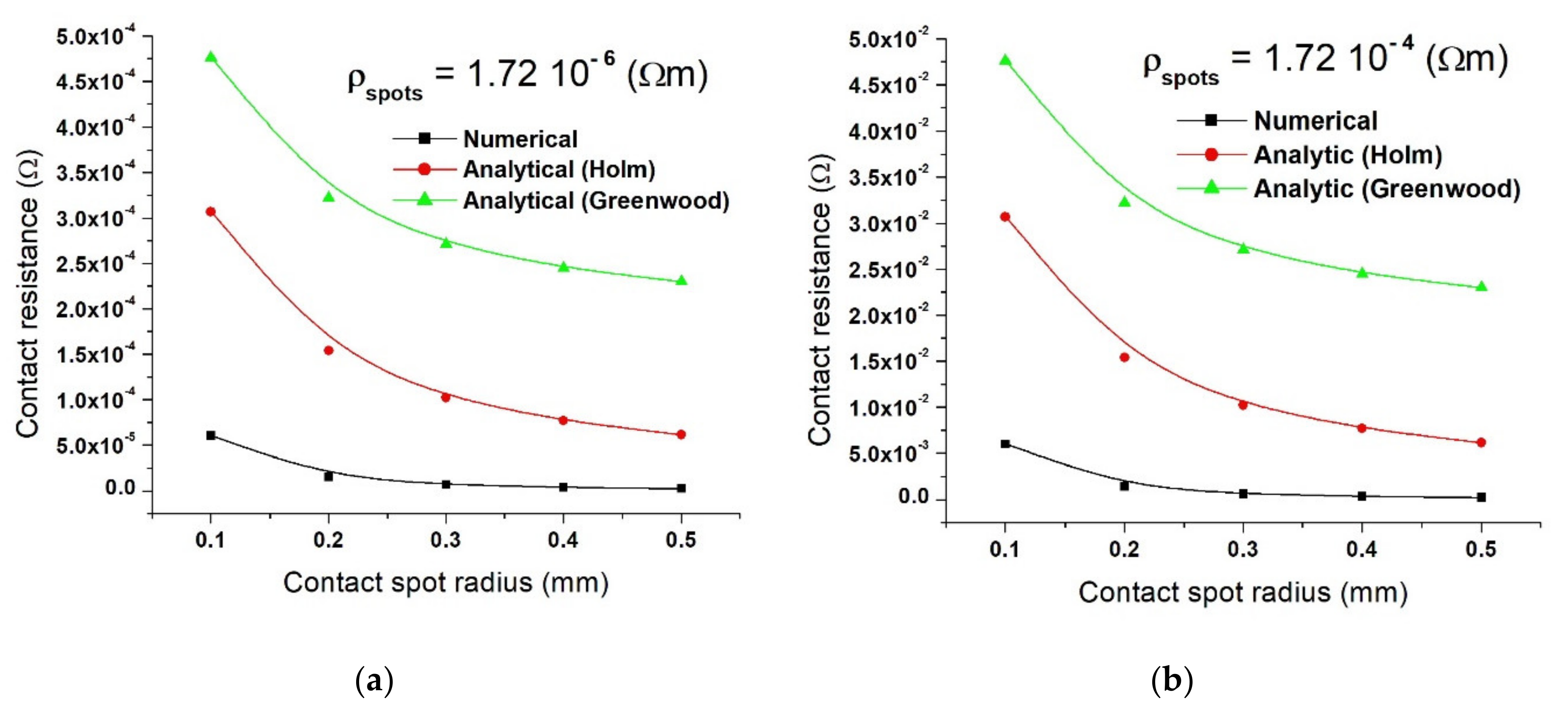
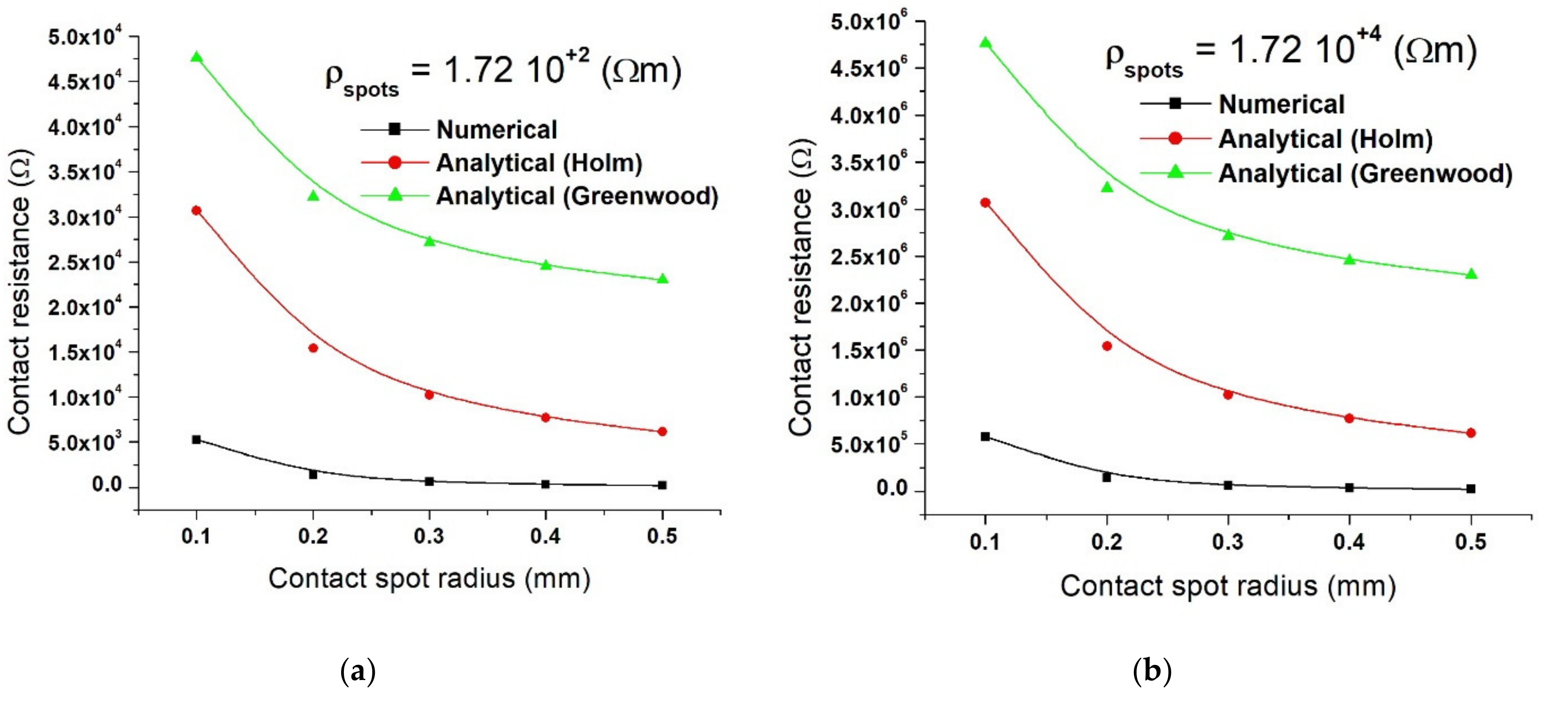
4. Results
5. Discussion
6. Conclusions
Author Contributions
Funding
Institutional Review Board Statement
Informed Consent Statement
Data Availability Statement
Conflicts of Interest
References
- Liu, M. A New Method for Measuring Contact Resistance; Beijing Orient Institute of Measurement & Test Chinese Academy of Space Technology: Bejing, China, 2005. [Google Scholar]
- Connectors: Technologies and Trends. Available online: https://www.zvei.org/fileadmin/user_upload/Presse_und_Medien/Publikationen/2016/November/Connectors_Technologies-and-Trends_engl/2016-11_Imagebroschuere_Steckverbinder_engl.pdf (accessed on 9 March 2022).
- Dankat, G.G.; Dobre, A.A.; Dumitran, L.M. Influence of Ageing on Electrothermal Condition of Low Current Contact. In Proceedings of the 2021 12th International Symposium on Advanced Topics in Electrical Engineering (ATEE), Bucharest, Romania, 25–27 March 2021; pp. 1–6. [Google Scholar]
- Holm, R. Electric Contacts, Theory and Application, 4th ed.; Springer: Berlin/Heidelberg, Germany, 1967. [Google Scholar]
- Greenwood, J.A. Constriction resistance and the real area of contact. Br. J. Appl. Phys. 1966, 17, 1621–1632. [Google Scholar] [CrossRef]
- Boyer, L. Contact resistance calculations: Generalizations of Greenwood’s formula including interface films. IEEE Trans. Compon. Packag. Technol. 2001, 24, 50–58. [Google Scholar] [CrossRef]
- Nakamura, M. Constriction resistance of conducting spots by the boundary element method. IEEE Trans. Compon. Hybrids Manuf. Technol. 1993, 16, 339–343. [Google Scholar] [CrossRef]
- Nakamura, M.; Minowa, I. Film resistance and constriction effect of current in a contact interface. IEEE Trans. Compon. Hybrids Manuf. Technol. 1989, 12, 109–113. [Google Scholar] [CrossRef]
- Nakamura, M.; Minowa, I. Computer simulation for the conductance of a contact interface. IEEE Trans. Compon. Hybrids Manuf. Technol. 1986, 9, 150–155. [Google Scholar] [CrossRef]
- Nakamura, M. Computer simulation for the constriction resistance depending on the form of conducting spots. IEEE Trans. Compon. Packag. Technol 1995, 18, 382–383. [Google Scholar] [CrossRef]
- Timsit, R.S. Electrical conduction through small contact spots. In Proceedings of the 50th IEEE Holm Conference on Electrical Contacts and the 22nd International Conference on Electrical Contacts, Seattle, WA, USA, 20–23 September 2004; pp. 184–191. [Google Scholar]
- Timsit, R.S. Electrical contact resistance: Properties of stationary interfaces. IEEE Trans. Compon. Packag. Technol. 1999, 22, 85–98. [Google Scholar] [CrossRef]
- Shujuan, W.; Fang, H.; Bonan, S.; Guofu, Z. Method for calculation of contact resistance and finite element simulation of contact temperature rise based on rough surface contact model. In Proceedings of the 26th International Conference on Electrical Contacts (ICEC 2012), Beijing, China, 14–17 May 2012; pp. 317–321. [Google Scholar]
- Ren, W.; Zhang, C.; Sun, X. Electrical Contact Resistance of Contact Bodies with Cambered Surface. IEEE Access 2020, 8, 93857–93867. [Google Scholar] [CrossRef]
- Lim, J.; Kim, H.; Kim, J.K.; Park, S.J.; Lee, T.H.; Yoon, S.W. Numerical and Experimental Analysis of Potential Causes Degrading Contact Resistances and Forces of Sensor Connectors for Vehicles. IEEE Access 2019, 7, 126530–126538. [Google Scholar] [CrossRef]
- Malucci, R.D. Multispot model of contacts based on surface features. In Proceedings of the 36th IEEE Holm Conference on Electrical Contacts, Montreal, QC, Canada, 20–24 August 1990; pp. 625–634. [Google Scholar]
- Malucci, R.D. Making contacts to aged surfaces. In Proceedings of the 38th IEEE Holm Conference on Electrical Contacts, Philadelphia, PA, USA, 18–21 October 1992; pp. 237–248. [Google Scholar]
- Fukuyama, Y.; Sakamoto, N.; Kaneko, N.; Kondo, T.; Toyoizumi, J.; Yudate, T. The effect of the distribution of a-spots in the peripheral part of an apparent contact point on the constriction resistance. In Proceedings of the 2017 IEEE Holm Conference on Electrical Contacts, Denver, CO, USA, 10–13 September 2017; pp. 302–305. [Google Scholar] [CrossRef]
- Swingler, J.; McBride, J.W. Fretting and the reliability of multi-contact connector terminals. IEEE Trans. Compon. Package Technol. 2002, 25, 670–676. [Google Scholar] [CrossRef]
- Acura TL Corroded/Burnt AC Blower Wire Harness Connector. Available online: https://joshsworld.com/cars/corroded-burnt-ac-blower-connector/ (accessed on 9 March 2022).
- BMW 7 Series. Available online: https://widnesautoelectrical.co.uk/bmw-7-series/ (accessed on 9 March 2022).
- Swingler, J.; McBride, J.W.; Maul, C. The degradation of road-tested automotive connectors. IEEE Trans. Compon. Package Technol. 2000, 23, 157–164. [Google Scholar] [CrossRef]
- Jedrzejczyk, P. Analyse and Quantification of Electrical Contacts Endurance under Fretting Loadings. Ph.D. Thesis, Politechnika Lodzka, Lodz, Poland, 2010. [Google Scholar]
- Su, B.; Qu, J. Electrical contact resistance of silver with different coatings. In Proceedings of the International Symposium on Advanced Packaging Materials: Processes, Properties, and Interfaces, Irvine, CA, USA, 16–18 March 2005; pp. 75–78. [Google Scholar] [CrossRef]
- Shibata, Y.; Oohira, S.; Masui, S.; Sawada, S.; Iida, K.; Tamai, T.; Hattori, Y. Detailed analysis of contact resistance of fretting corrosion track for the tin-plated contacts. In Proceedings of the 26th International Conference on Electrical Contacts (ICEC 2012), Beijing, China, 14–17 May 2012; pp. 228–232. [Google Scholar] [CrossRef]
- Fukuyama, Y.; Sakamoto, N.; Kaneko, N.-H.; Kondo, T.; Onuma, M. Constriction resistance of physical simulated electrical contacts with nanofabrication. In Proceedings of the 2014 IEEE 60th Holm Conference on Electrical Contacts (Holm), New Orleans, LA, USA, 12–15 October 2014; pp. 1–5. [Google Scholar] [CrossRef]


Publisher’s Note: MDPI stays neutral with regard to jurisdictional claims in published maps and institutional affiliations. |
© 2022 by the authors. Licensee MDPI, Basel, Switzerland. This article is an open access article distributed under the terms and conditions of the Creative Commons Attribution (CC BY) license (https://creativecommons.org/licenses/by/4.0/).
Share and Cite
Dankat, G.G.; Dumitran, L.M. Computation of the Electrical Resistance of a Low Current Multi-Spot Contact. Materials 2022, 15, 2056. https://doi.org/10.3390/ma15062056
Dankat GG, Dumitran LM. Computation of the Electrical Resistance of a Low Current Multi-Spot Contact. Materials. 2022; 15(6):2056. https://doi.org/10.3390/ma15062056
Chicago/Turabian StyleDankat, Gideon Gwanzuwang, and Laurentiu Marius Dumitran. 2022. "Computation of the Electrical Resistance of a Low Current Multi-Spot Contact" Materials 15, no. 6: 2056. https://doi.org/10.3390/ma15062056
APA StyleDankat, G. G., & Dumitran, L. M. (2022). Computation of the Electrical Resistance of a Low Current Multi-Spot Contact. Materials, 15(6), 2056. https://doi.org/10.3390/ma15062056