
Low-Temperature Cu/SiO2 Hybrid Bonding with Low Contact Resistance Using (111)-Oriented Cu Surfaces

 , , ,
, , , 

Abstract
:1. Introduction
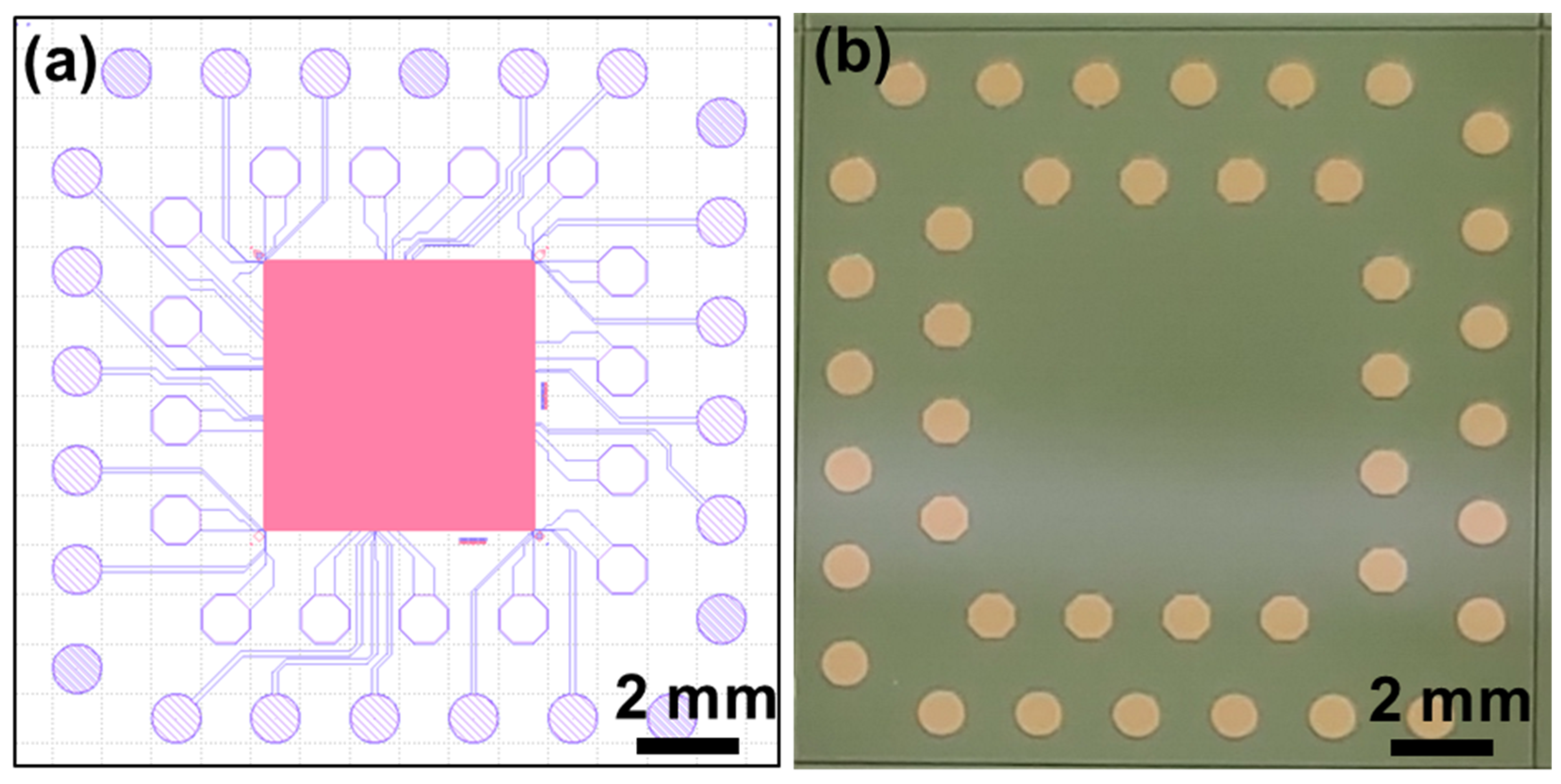
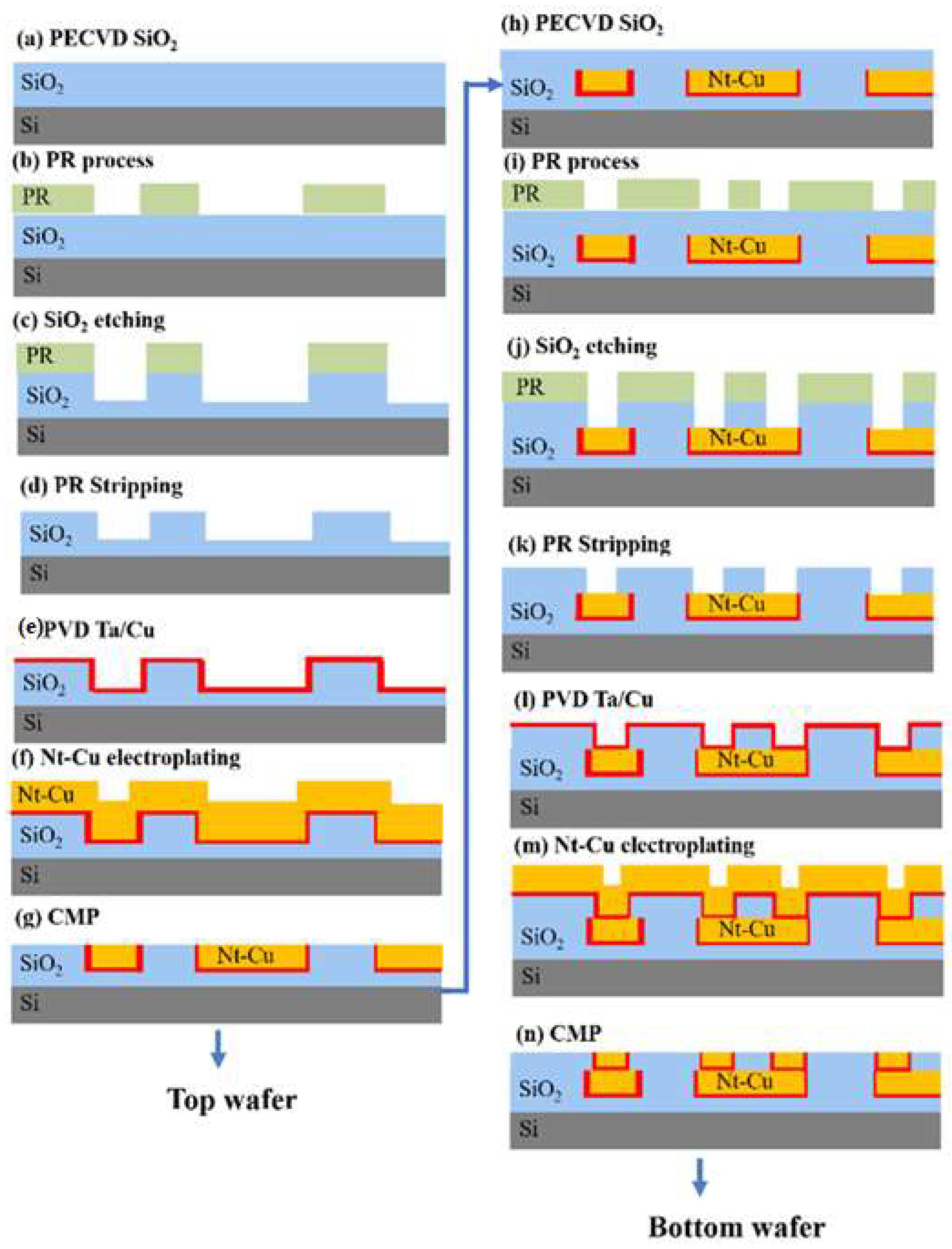
2. Materials and Methods
3. Results
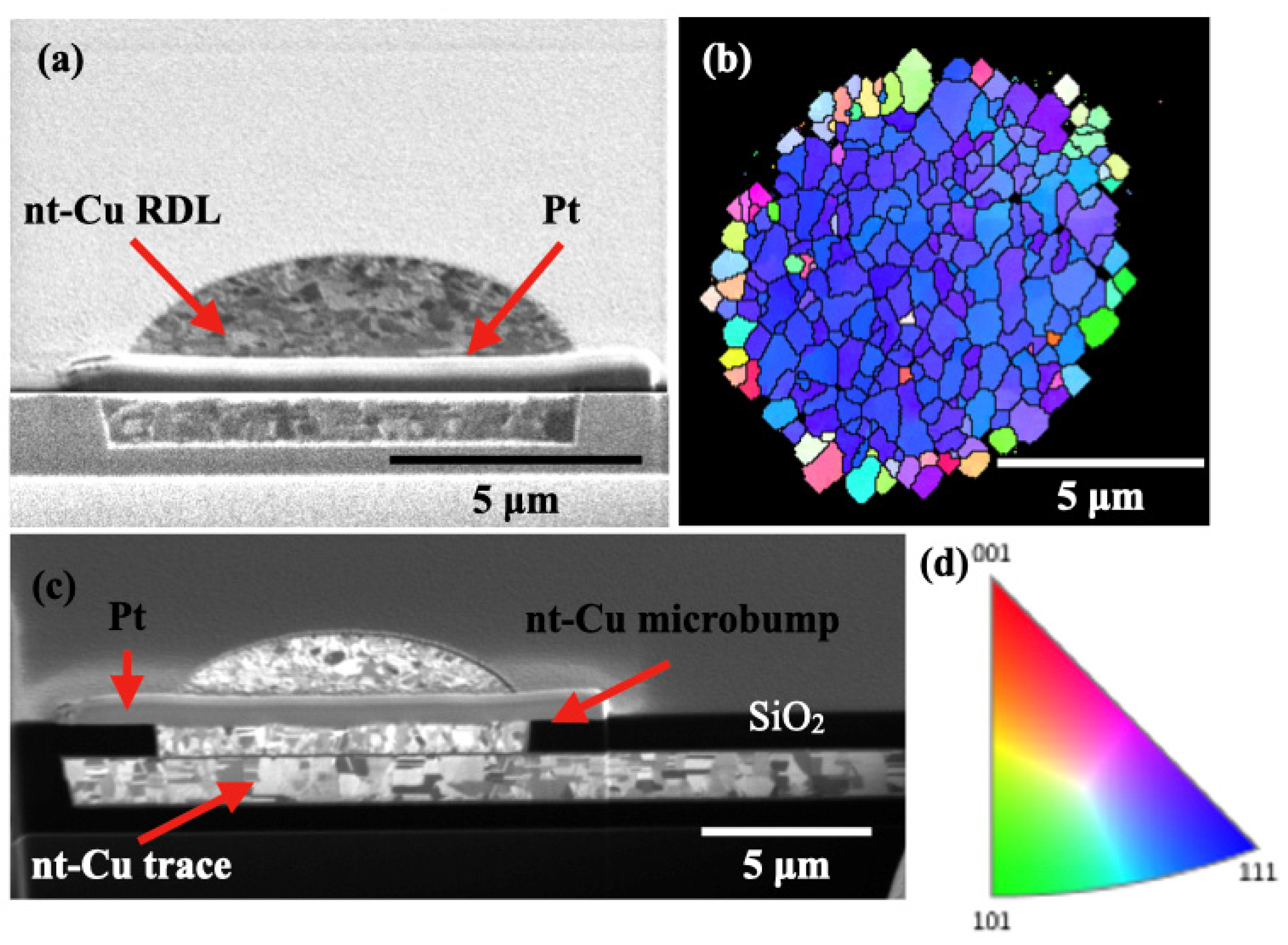
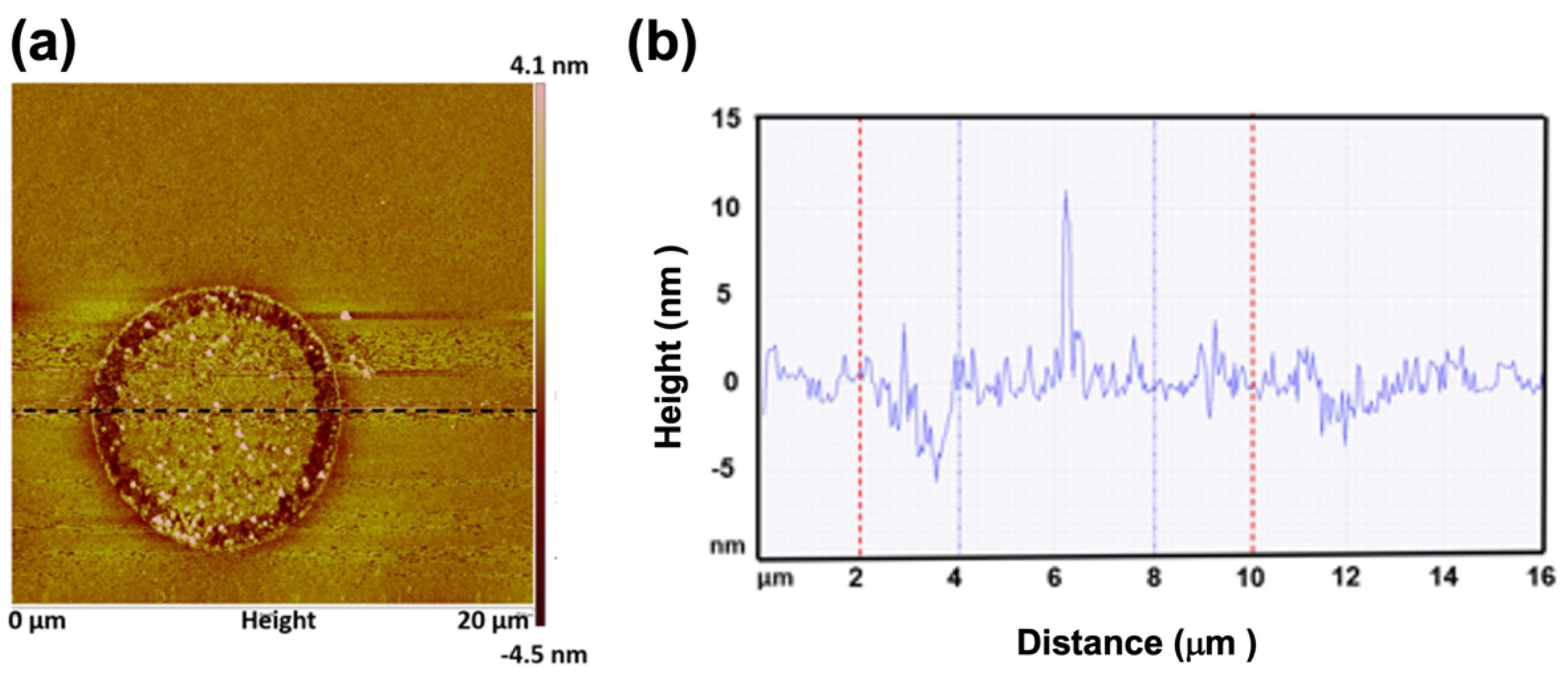
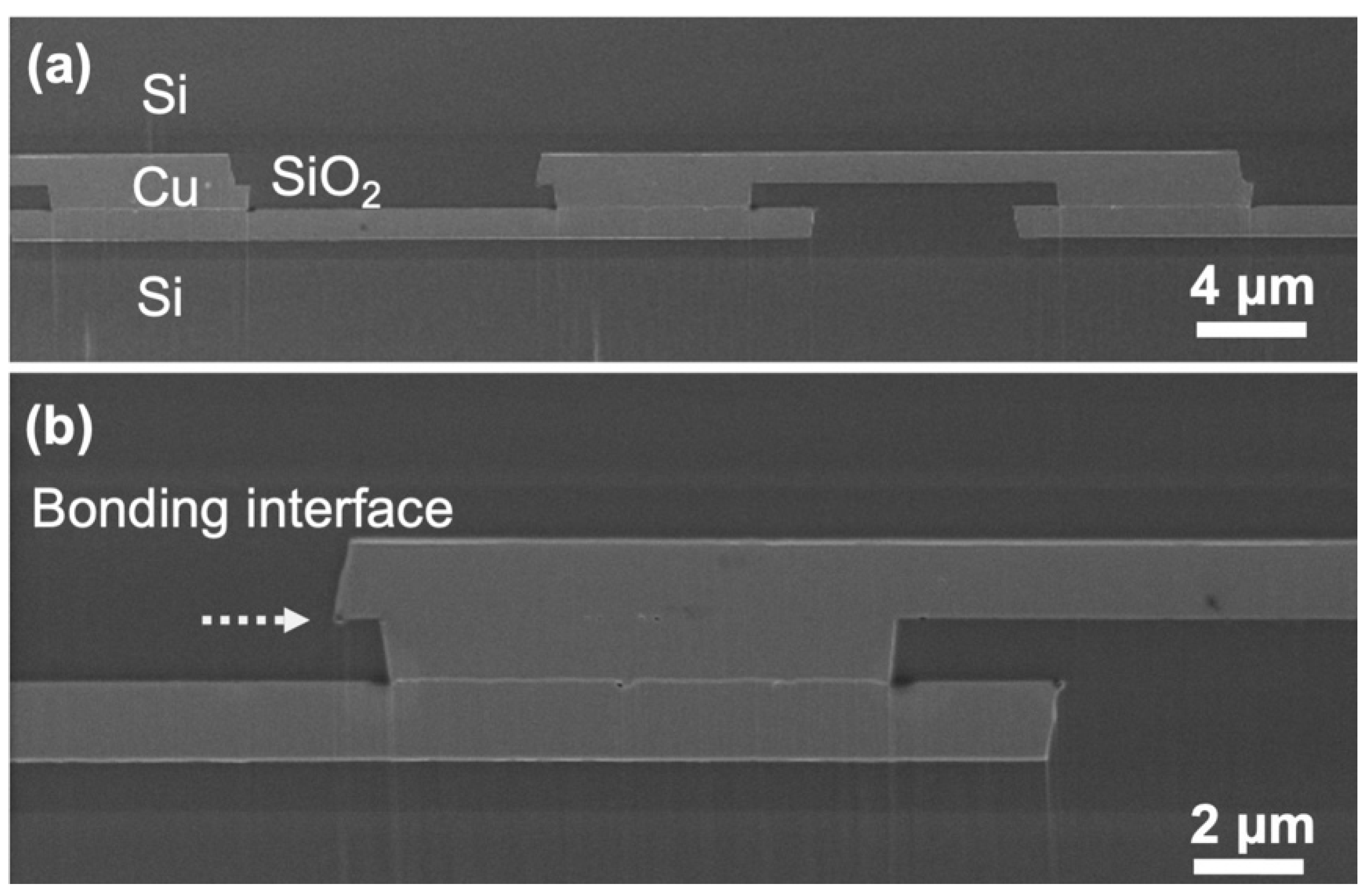
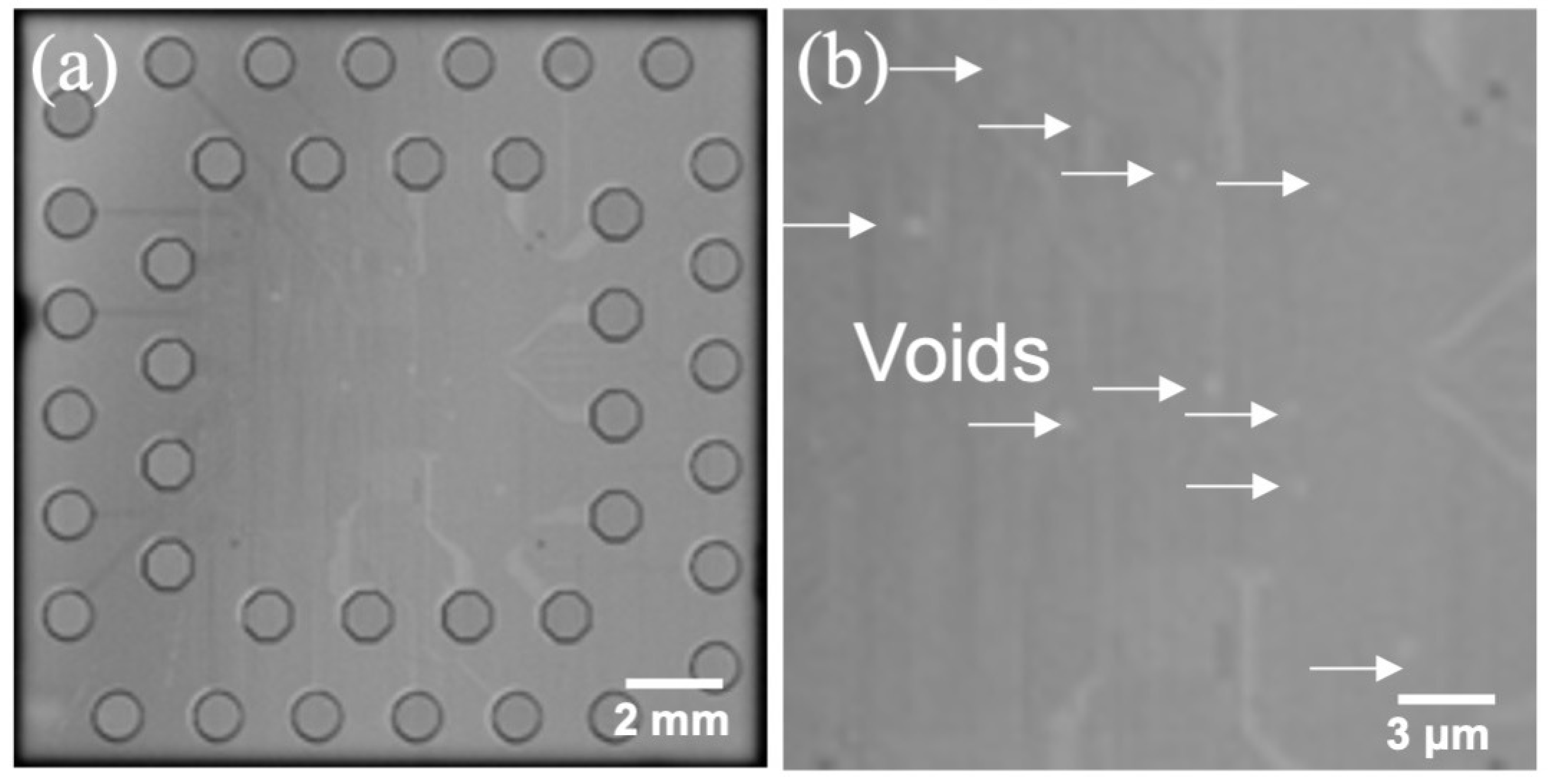
3.1. Microstructural Characterization
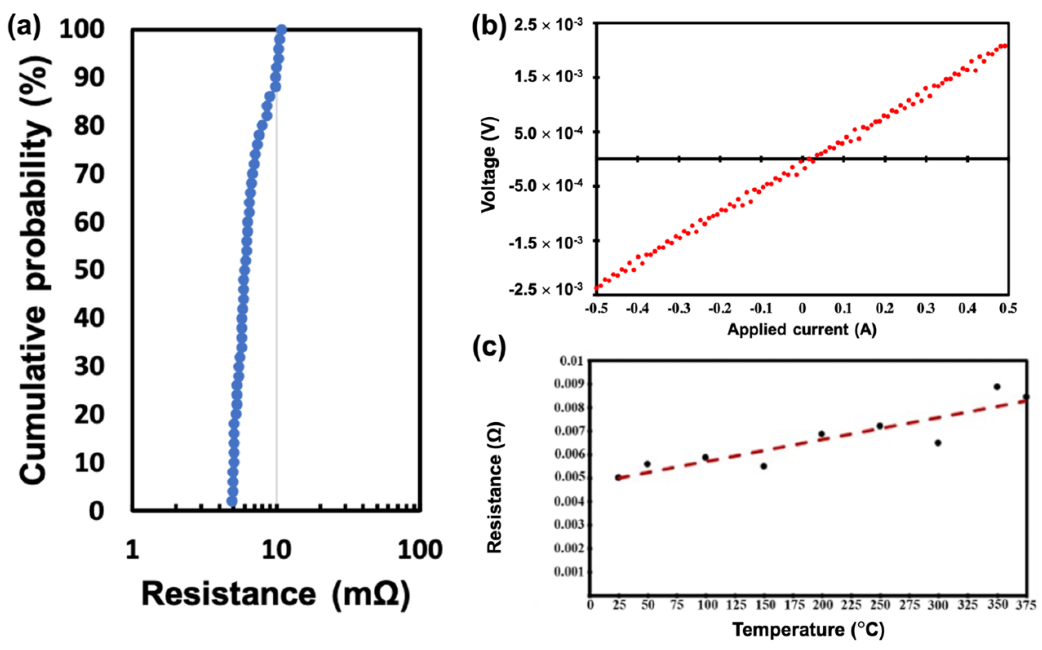
3.2. Electrical Resistance Measured by Kelvin Probes
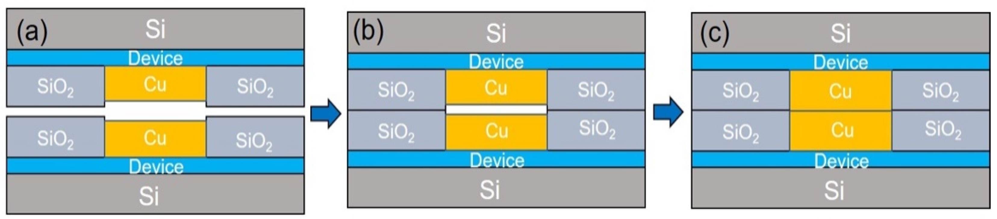
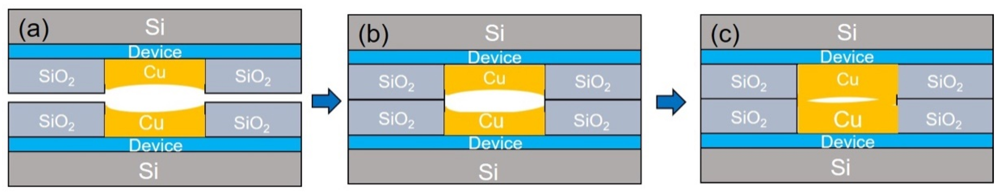
3.3. Mechanism for Cu/SiO2 Hybrid Bonding
4. Conclusions
Author Contributions
Funding
Data Availability Statement
Acknowledgments
Conflicts of Interest
References
- Chen, M.-F.; Chen, F.-C.; Chiou, W.-C.; Yu, D.C.H. System on Integrated Chips (SoIC(TM) for 3D Heterogeneous Integration. In Proceedings of the 2019 IEEE 69th Electronic Components and Technology Conference (ECTC), Las Vegas, NV, USA, 28–31 May 2019; pp. 594–599. [Google Scholar] [CrossRef]
- Chen, Y.H.; Yang, C.A.; Kuo, C.C.; Chen, M.F.; Tung, C.H.; Chiou, W.C.; Yu, D. Ultra high density SoIC with sub-micron bond pitch. In Proceedings of the 2020 IEEE 70th Electronic Components and Technology Conference (ECTC), Orlando, FL, USA, 3–30 June 2020; pp. 576–581. [Google Scholar] [CrossRef]
- Tu, K.-N.; Chen, C.; Chen, H.-M. Electronic Packaging Science and Technology, 1st ed.; John Wiley & Sons: Hoboken, NJ, USA, 2022; pp. 19–57. [Google Scholar]
- Kagawa, Y.; Fujii, N.; Aoyagi, K.; Kobayashi, Y.; Nishi, S.; Todaka, N.; Hirayama, T. Novel stacked CMOS image sensor with advanced Cu2Cu hybrid bonding. In Proceedings of the 2016 IEEE International Electron Devices Meeting (IEDM), San Francisco, CA, USA, 3–7 December 2016; pp. 8–14. [Google Scholar] [CrossRef]
- Beyne, E.; Kim, S.W.; Peng, L.; Heylen, N.; De Messemaeker, J.; Okudur, O.O.; Beyer, G. Scalable, sub 2 μm pitch, Cu/SiCN to Cu/SiCN hybrid wafer-to-wafer bonding technology. In Proceedings of the 2017 IEEE International Electron Devices Meeting (IEDM), San Francisco, CA, USA, 2–6 December 2017; pp. 32–34. [Google Scholar] [CrossRef]
- Jourdon, J.; Lhostis, S.; Moreau, S.; Chossat, J.; Arnoux, M.; Sart, C.; Cheramy, S. Hybrid bonding for 3D stacked image sensors: Impact of pitch shrinkage on interconnect robustness. In Proceedings of the 2018 IEEE International Electron Devices Meeting (IEDM), San Francisco, CA, USA, 1–5 December 2018; pp. 7–13. [Google Scholar] [CrossRef]
- Chou, T.C.; Yang, K.M.; Li, J.C.; Yu, T.Y.; Chung, Y.T.; Ko, C.T.; Chen, K.N. Non-planarization Cu-Cu direct bonding and gang bonding with low temperature and short duration in ambient atmosphere. In Proceedings of the 2019 IEEE International Electron Devices Meeting (IEDM), San Francisco, CA, USA, 7–11 December 2019; pp. 5–15. [Google Scholar] [CrossRef]
- Kim, S.W.; Fodor, F.; Heylen, N.; Iacovo, S.; De Vos, J.; Miller, A.; Beyne, E. Novel Cu/SiCN surface topography control for 1 μm pitch hybrid wafer-to-wafer bonding. In Proceedings of the 2020 IEEE 70th Electronic Components and Technology Conference (ECTC), Orlando, FL, USA, 3–30 June 2020; pp. 216–222. [Google Scholar] [CrossRef]
- Lu, L.; Shen, Y.; Chen, X.; Qian, L.; Lu, K. Ultrahigh strength and high electrical conductivity in copper. Science 2004, 304, 422–426. [Google Scholar] [CrossRef] [PubMed] [Green Version]
- Tseng, C.H.; Tu, K.N.; Chen, C. Comparison of oxidation in uni-directionally and randomly oriented Cu films for low temperature Cu-to-Cu direct bonding. Sci. Rep. 2018, 8, 10671. [Google Scholar] [CrossRef] [PubMed]
- Chen, K.C.; Wu, W.W.; Liao, C.N.; Chen, L.J.; Tu, K.N. Observation of atomic diffusion at twin-modified grain boundaries in copper. Science 2008, 321, 1066–1069. [Google Scholar] [CrossRef] [PubMed] [Green Version]
- Hsiao, H.Y.; Liu, C.M.; Lin, H.W.; Liu, T.C.; Lu, C.L.; Huang, Y.S.; Tu, K.N. Unidirectional growth of microbumps on (111)-oriented and nanotwinned copper. Science 2012, 336, 1007–1010. [Google Scholar] [CrossRef] [PubMed] [Green Version]
- Liu, C.M.; Lin, H.W.; Huang, Y.S.; Chu, Y.C.; Chen, C.; Lyu, D.R.; Tu, K.N. Low-temperature direct copper-to-copper bonding enabled by creep on (111) surfaces of nanotwinned Cu. Sci. Rep. 2015, 5, 9734. [Google Scholar] [CrossRef] [PubMed] [Green Version]
- Liu, C.M.; Lin, H.W.; Chu, Y.C.; Chen, C.; Lyu, D.R.; Chen, K.N.; Tu, K.N. Low-temperature direct copper-to-copper bonding enabled by creep on highly (111)-oriented Cu surfaces. Scr. Mater. 2014, 78, 65–68. [Google Scholar] [CrossRef]
- Shie, K.C.; Gusak, A.M.; Tu, K.N.; Chen, C. A kinetic model of copper-to-copper direct bonding under thermal compression. J. Mater. Res. Technol. 2012, 15, 2332–2344. [Google Scholar] [CrossRef]
- Liu, H.C.; Gusak, A.M.; Tu, K.N.; Chen, C. Interfacial void ripening in Cu-Cu joints. Mater. Charact. 2021, 181, 111459. [Google Scholar] [CrossRef]
- Chiu, W.L.; Lee, O.H.; Chiang, C.W.; Chang, H.H. Low Temperature Wafer-To-Wafer Hybrid Bonding by Nanotwinned Copper. In Proceedings of the 2021 IEEE 71st Electronic Components and Technology Conference (ECTC), San Diego, CA, USA, 1 June–4 July 2021; pp. 365–370. [Google Scholar] [CrossRef]
- Shie, K.C.; Hsu, P.N.; Li, Y.J.; Tu, K.N.; Lin, B.T.H.; Chang, C.C.; Chen, C. Electromigration and temperature cycling tests of Cu-Cu joints fabricated by instant copper direct bonding. In Proceedings of the 2021 IEEE 71st Electronic Components and Technology Conference (ECTC), San Diego, CA, USA, 1 June–4 July 2021; pp. 995–1000. [Google Scholar] [CrossRef]
- Tran, D.P.; Chen, K.J.; Tu, K.N.; Chen, C.; Chen, Y.T.; Chung, S. Electrodeposition of slanted nanotwinned Cu foils with high strength and ductility. Electrochim. Acta 2021, 389, 138640. [Google Scholar] [CrossRef]
- Ong, J.J.; Tran, D.P.; Yang, S.C.; Shie, K.C.; Chen, C. Shearing characteristics of Cu-Cu joints fabricated by two-step process using highly <111>-oriented nanotwinned Cu. Metals 2021, 11, 1864. [Google Scholar] [CrossRef]
- Cheng, H.Y.; Tran, D.P.; Tu, K.N.; Chen, C. Effect of deposition temperature on mechanical properties of nanotwinned Cu fabricated by rotary electroplating. Mater. Sci. Eng. A 2021, 811, 141065. [Google Scholar] [CrossRef]
- Li, Y.J.; Tu, K.N.; Chen, C. Tensile properties and thermal stability of unidirectionally <111>-oriented nanotwinned and <110>-oriented microtwinned copper. Materials 2020, 13, 1211. [Google Scholar] [CrossRef] [Green Version]
- Tseng, I.H.; Hsu, P.N.; Lu, T.L.; Tu, K.N.; Chen, C. Electromigration failure mechanisms of <111>-oriented nanotwinned Cu redistribution lines with polyimide capping. Results Phys. 2021, 24, 104154. [Google Scholar] [CrossRef]
- Chen, K.N.; Fan, A.; Tan, C.S.; Reif, R. Contact resistance measurement of bonded copper interconnects for three-dimensional integration technology. IEEE Electron. Device Lett. 2004, 25, 10–12. [Google Scholar] [CrossRef]
- Gueguen, P.; Di Cioccio, L.; Morfouli, P.; Zussy, M.; Dechamp, J.; Bally, L.; Clavelier, L. Copper direct bonding: An innovative 3D interconnect. In Proceedings of the 2010 Proceedings 60th Electronic Components and Technology Conference (ECTC), Las Vegas, NV, USA, 1–4 June 2010; pp. 878–883. [Google Scholar] [CrossRef]
- Tan, C.S.; Peng, L.; Li, H.Y.; Lim, D.F.; Gao, S. Wafer-on-wafer stacking by bumpless Cu–Cu bonding and its electrical characteristics. IEEE Electron. Device Lett. 2011, 32, 943–945. [Google Scholar] [CrossRef]
- Peng, L.; Li, H.Y.; Lim, D.F.; Lo, G.Q.; Kwong, D.L.; Tan, C.S. High density bump-less Cu-Cu bonding with enhanced quality achieved by pre-bonding temporary passivation for 3D wafer stacking. In Proceedings of the 2011 International Symposium on VLSI Technology, Systems and Applications, Hsinchu, Taiwan, 25–27 April 2011; pp. 1–2. [Google Scholar] [CrossRef]
- Shigetou, A.; Itoh, T.; Sawada, K.; Suga, T. Bumpless interconnect of 6-µm-pitch Cu electrodes at room temperature. IEEE Trans. Adv. Packag. 2008, 31, 473–478. [Google Scholar] [CrossRef]
- Beilliard, Y.; Moreau, S.; Di Cioccio, L.; Coudrain, P.; Romano, G.; Nowodzinski, A.; Signamarcheix, T. Advances toward reliable high density Cu-Cu interconnects by Cu-SiO2 direct hybrid bonding. In Proceedings of the 2014 International 3D Systems Integration Conference (3DIC), Kinsdale, Ireland, 1–3 December 2014; pp. 1–8. [Google Scholar] [CrossRef]
- Jansen, F.; Machonkin, M.A.; Palmieri, N.; Kuhman, D. Thermal expansion and elastic properties of plasma-deposited amorphous silicon and silicon oxide films. Appl. Phys. Lett. 1987, 50, 1059–1061. [Google Scholar] [CrossRef]


Publisher’s Note: MDPI stays neutral with regard to jurisdictional claims in published maps and institutional affiliations. |
© 2022 by the authors. Licensee MDPI, Basel, Switzerland. This article is an open access article distributed under the terms and conditions of the Creative Commons Attribution (CC BY) license (https://creativecommons.org/licenses/by/4.0/).
Share and Cite
Ong, J.-J.; Chiu, W.-L.; Lee, O.-H.; Chiang, C.-W.; Chang, H.-H.; Wang, C.-H.; Shie, K.-C.; Yang, S.-C.; Tran, D.-P.; Tu, K.-N.; et al. Low-Temperature Cu/SiO2 Hybrid Bonding with Low Contact Resistance Using (111)-Oriented Cu Surfaces. Materials 2022, 15, 1888. https://doi.org/10.3390/ma15051888
Ong J-J, Chiu W-L, Lee O-H, Chiang C-W, Chang H-H, Wang C-H, Shie K-C, Yang S-C, Tran D-P, Tu K-N, et al. Low-Temperature Cu/SiO2 Hybrid Bonding with Low Contact Resistance Using (111)-Oriented Cu Surfaces. Materials. 2022; 15(5):1888. https://doi.org/10.3390/ma15051888
Chicago/Turabian StyleOng, Jia-Juen, Wei-Lan Chiu, Ou-Hsiang Lee, Chia-Wen Chiang, Hsiang-Hung Chang, Chin-Hung Wang, Kai-Cheng Shie, Shih-Chi Yang, Dinh-Phuc Tran, King-Ning Tu, and et al. 2022. "Low-Temperature Cu/SiO2 Hybrid Bonding with Low Contact Resistance Using (111)-Oriented Cu Surfaces" Materials 15, no. 5: 1888. https://doi.org/10.3390/ma15051888
APA StyleOng, J.-J., Chiu, W.-L., Lee, O.-H., Chiang, C.-W., Chang, H.-H., Wang, C.-H., Shie, K.-C., Yang, S.-C., Tran, D.-P., Tu, K.-N., & Chen, C. (2022). Low-Temperature Cu/SiO2 Hybrid Bonding with Low Contact Resistance Using (111)-Oriented Cu Surfaces. Materials, 15(5), 1888. https://doi.org/10.3390/ma15051888