Abstract
We adopted (111)-oriented Cu with high surface diffusivity to achieve low-temperature and low-pressure Cu/SiO2 hybrid bonding. Electroplating was employed to fabricate arrays of Cu vias with 78% (111) surface grains. The bonding temperature can be lowered to 200 °C, and the pressure is as low as 1.06 MPa. The bonding process can be accomplished by a 12-inch wafer-to-wafer scheme. The measured specific contact resistance is 1.2 × 10⁻⁹ Ω·cm2, which is the lowest value reported in related literature for Cu-Cu joints bonded below 300 °C. The joints possess excellent thermal stability up to 375 °C. The bonding mechanism is also presented to provide more understanding on hybrid bonding.
1. Introduction
As the evolution of AI and high-performance computing (HPC) devices needs more input and output (I/O) numbers, fine-pitch packaging techniques such as Cu-Cu bonding [1,2,3] or Cu/dielectric hybrid bonding is needed urgently. In addition, 3D IC packaging is at the core of development for advanced package technology to provide high bandwidth and low power consumption. Nowadays, flip-chip solder micro-joints are commonly used for vertical interconnects. However, the size of micro-joints cannot be scaled down to 10 μm due to side wetting of solders and bridging failures.
Cu/oxide hybrid bonding, on the other hand, with oxide or SiCN dielectrics has been adopted for fine-pitch packaging and can be scaled down continuously below the submicron scale [4,5,6,7,8]. Furthermore, copper shows low electrical resistivity (ρ) of 1.7 × 10⁻⁶ Ω·cm2 which is a constant that would be varied by different materials. Thus, it would affect the resistance with the cross-sectional area of the materials that current flows through. On the other hand, silicon oxide has been an optimal dielectric for copper hybrid bonding due to its low coefficient of thermal expansion (CTE) and high bonding energy. However, the current bonding temperature is around 300 °C, which is too high for high-bandwidth memories. Therefore, to reduce thermal budget and thermal stress and to increase alignment accuracy, it is necessary to lower bonding temperature.
Highly <111>-oriented nanotwinned (nt) Cu possesses low resistivity, low oxidation rate, and high electromigration resistance [9,10,11,12]. More importantly, the (111) surface has the highest diffusivity among all the crystallographic planes in face-centered cubic (FCC) crystals, this is due to the fact that the (111) plane is the most densely packed surface which contributes to high atomic diffusivity [13,14]. The bonding mechanism is attributed to surface creep, which is atomic diffusion under stress gradient at elevated temperatures [15]. Thus, direct bonding can be completed at low temperatures. The size distribution of voids and evolution due to the ripening effect during bonding have also been reported [16]. With the advantage of highly <111> nt-Cu, one can further lower the bonding temperature to 200 °C [17]. However, there is no study reporting the electrical characteristics of the nt-Cu/SiO2 hybrid bonds.
In this paper, we adopt the highly <111>-nanotwinned Cu (nt-Cu) and SiO2 dielectrics to lower the bonding temperature and pressure. Kelvin and cross-bar structures were designed to measure the electrical resistance and specific contact resistance. The results show that excellent bonding interfaces can be obtained at 200 °C under 1.06 MPa. The electrical resistance is quite stable from 25 °C to 375 °C. Furthermore, the nt-Cu/SiO2 hybrid bonds possess very low resistance and very low specific contact resistance.
2. Materials and Methods
The bonding schemes are 12-inch wafer-to-wafer. Initially, we fabricated 20 μm pitch Cu bumps with Cu redistribution layer (RDL) on top wafers and Cu RDL/microbumps on bottom wafers. Figure 1a–g displays the schematic processes for preparing the top wafers. A SiO2 film with 2 μm in thickness was initially deposited by plasma-enhanced chemical vapor deposition (PECVD, AMAT Producer SE, Applied Materials, Santa Clara, CA, USA), followed by lithography(SUSS Aligner MA300, SUSS MicroTec SE, Garching, Germany) and etching to define patterns. A Ta/Cu seed layer was deposited by physical vapor deposition. Highly (111)-oriented nt-Cu with 2 μm thickness was electroplated with bottom wafer fabrication, additional Cu vias measuring 8 μm in diameter were fabricated on the Cu RDL. Finally, by using chemical mechanical planarization (CMP, AMAT Reflexion LK Applied Materials, Santa Clara, CA, USA), the co-planarized nt-Cu/SiO2 surfaces were obtained, as depicted in Figure 1h–n.
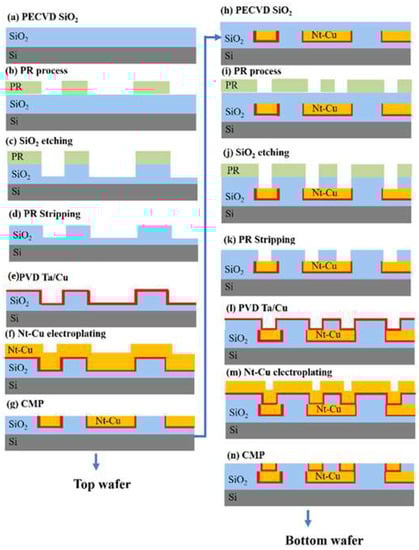
Figure 1.
Schematic fabrication processes for top and bottom wafers.
To achieve excellent recess control on the nt-Cu and SiO2, CMP was used to remove excess Cu and to control dishing on the bonding interface by a two-step process [17]. Proper dishing is desired for Cu/SiO2 hybrid bonding because the coefficient of thermal expansion for Cu is higher than that of SiO2. We will explain the details of the bonding mechanism later. With the two-step CMP process, the dishing performance can be well controlled within a few nanometers.
For wafer-to-wafer hybrid bonding process, the as-prepared top and bottom wafers were cleaned by N2 plasma, followed by exposed in vacuum ambient (~10−3 mbar) under a contact force of 75 kN which is corresponding to 1.06 MPa and held at room temperature for pre-bonding, and the bonded pair was bonded at 200 °C for 1 h. The elevated temperature and pressure were further induced to the Cu surface to contact and begin diffusion bonding at the interface. To strengthen the bonding pair, post-annealing at 200 °C for 4 h was conducted, which may further improve both bonding strength and electrical properties. After the bonding process by a wafer level bonder (SUSS XBC-300, SUSS MicroTec SE, Garching, Germany) which the alignment accuracy can be controlled within ±1 μm, wafer grinding was conducted to thin down the top Si wafer to 20 μm. To expose the probing Cu pad, additional lithography and etching processes were conducted on the top wafer to open the probing pads. A dicing process was performed to slice 15 × 15 mm2 specimens for electrical and reliability tests. Figure 2a shows the designed layout for the test vehicle measuring 6 × 6 mm2 for the top die and 15 × 15 mm2 for the bottom die. There are 8000 Cu-Cu joints in each die. Figure 2b shows the optical photo for the fabricated die pair after the etching of the top die and the Cu probing pads exposed for electrical measurement.
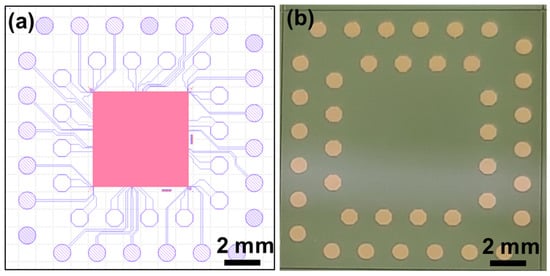
Figure 2.
(a) Layout design for the test vehicles with top die bonded to bottom die. (b) Photo of a diced die.
For microstructure analysis, electron back-scattered diffraction (EBSD, JEOL JSM-7800F, Tokyo, Japan) was used to analyze grain size and crystal orientation. Microstructures and bonding quality were characterized by a focused ion beam (FIB, FEI Nova 2000, Hillsboro, OR, USA). Additionally, an atomic force microscope (AFM, Bruker Innova SPM, Billerica, MA, USA) was employed to obtain the random roughness patterns and determine the surface roughness (Rq) of the nt-Cu vias. Confocal scanning acoustic microscopy (CSAM, Nordson SONOSCAN-Gen6, Elk Village, IL, USA) was used to examine voids non-destructively. For electrical resistance measurement, a source meter (Keithley 2700, Keithley, Instruments Cleveland, OH, USA) was adopted to measure the resistance of the Cu joints from −0.5 A to 0.5 A, and from room temperature to 375 °C. Kelvin probes were employed for the resistance measurement of a single Cu-Cu joint.
3. Results
3.1. Microstructural Characterization
The microstructures of the Cu pads after the CMP process were analyzed by FIB and EBSD. Figure 3a shows the cross-sectional FIB image of nt-Cu RDL on the top die before bonding. No obvious dishing was observed. The Pt layer was deposited to avoid damaging the Cu in the FIB during ion cutting. The plan-view EBSD shows 78% of the via surface is (111)-oriented grains, as shown in Figure 3b,c depicts the cross-sectional FIB for the nt-Cu microbump on the nt-Cu trace in the bottom die. The inverse pole figure is shown in Figure 3d. The nt-Cu trace was designed for the measurement of electrical resistance of the Cu-Cu joint.
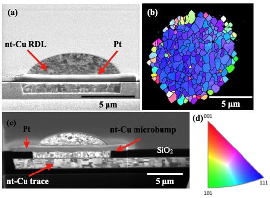
Figure 3.
Microstructural characterization on the Cu via and joints before bonding. (a) Cross-sectional FIB image of unbonded nt-Cu RDL in the top die. (b) Plan-view EBSD analysis for a typical Cu bump on the test vehicle shows 78% of the via surface is (111)-preferred grains. (c) Cross-sectional FIB for the nt-Cu microbump on the nt-Cu trace in the bottom die. (d) Inverse pole figure of Cu.
To facilitate hybrid bonding, the surface roughness of Cu and SiO2 need to be reduced by CMP to a few nanometers. Figure 4 shows the typical AFM results for a Cu via surrounded by SiO2 dielectrics. The root mean square averages of the individual heights and depths from the mean line (Rq) were measured for the Cu and SiO2 surface as 1.65 and 0.5 nm in average of six samples each, respectively. It is worth noting that the nt-Cu has a high hardness of 2.2 GPa, which minimizes the dishing after a CMP process. As shown in Figure 3a and Figure 4, the dishing/recess is quite uniform and can be controlled within 3 nm, which is good for bonding with a better interface geometry.
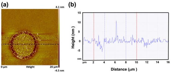
Figure 4.
(a) AFM topography and (b) the results of analyzed surface roughness show that the recess of a typical Cu bump is less than 3 nm and Rq is less than 2 nm.
It is reported that the Cu surface diffusivity on (111) planes is approximately 3–4 orders faster than that on (100) or (110) planes [13]. With ultra-high surface diffusivity, excellent Cu-Cu bonds can be achieved at 200 °C by wafer-to-wafer bonding. Such a bonding process with different adjustments of parameters was demonstrated to provide excellent mechanical properties [18,19,20,21,22] and high resistance in electromigration [18,23].
Confocal scanning acoustic microscopy (CSAM) was used to examine bonding quality non-destructively. The resolution we adopted is good enough to observe the unbonded area in a die. Figure 5a shows the CSAM image for a bonded die pair and the results show that more than 95% of the bonding area was well bonded. We have also enlarged the CSAM analyzed image and found that just a few small voids were observed as shown in Figure 5b.
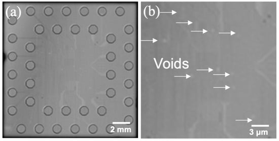
Figure 5.
(a) CSAM results for bonded dies showing more than 95% areas are well bonded. (b) Enlarged image of bonded area with small voids indicated by pointed arrows.
Then the specimens were ion-milled by FIB for further bonding interface examination. Figure 6a shows cross-sectional SEM, respectively. Figure 6b presents an enlarged SEM image for a single Cu-Cu joint, which shows the Cu-Cu and SiO2-SiO2 are well bonded at this condition without obvious voids or cracks.
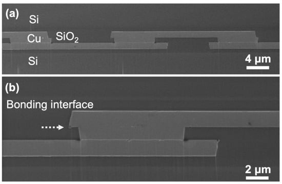
Figure 6.
(a) SEM and (b) enlarged SEM images showing a row of Cu-Cu joints surrounded by SiO2 dielectrics.
3.2. Electrical Resistance Measured by Kelvin Probes
The nt-Cu/SiO2 hybrid bonds possess excellent electrical properties, although they were bonded at a low temperature of 200 °C. Electrical resistance was measured by four-point probes after the post-annealing process. Figure 7a shows the measured resistance for a Kelvin structure by wafer-to-wafer hybrid bonding approach. The total number of measured contact structures is 50 and the average resistance is 6.7 mΩ, while small variations in resistance of ±1.75 mΩ were observed. Similarly, crossbar modified Kelvin structures were also fabricated by Cu-Cu bonding, thus the bonding area can be fixed at 10 μm × 8 μm and the problem of misalignment can be ignored. The average resistance of 50 joints is 1.5 mΩ, which corresponds to a specific contact resistance of 1.2 × 10⁻⁹ Ω·cm2. So far, this value is the lowest among all the literature values for Cu-Cu joints bonded below 300 °C. Table 1 summarizes the corresponding published values with similar contact areas but at various temperatures. Usually, in order to achieve low specific contact resistance, the temperature for the bonding has to exceed 250 °C. By using the highly (111)-oriented Cu surface, low temperature bonding with low specific contact resistance can be achieved due to the high surface diffusivity and low oxidation rate.
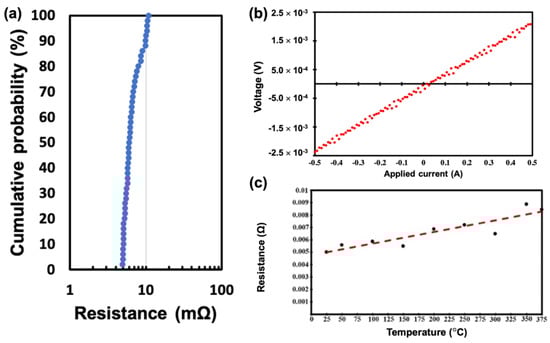
Figure 7.
(a) Measured cumulative resistance for single Cu-Cu joint by four-point probes; (b) I–V curves; (c) Resistance against measured temperatures from 25 °C to 375 °C.

Table 1.
List of measured specific contact resistances from literature.
3.3. Mechanism for Cu/SiO2 Hybrid Bonding
The mechanism for the Cu/SiO2 hybrid bonding is described below. The key step for the hybrid bonding is to control the height and shape of the Cu recess precisely. Figure 8 illustrates the schematic diagram for the hybrid bonding mechanism. After the CMP process, the height of the Cu via should be slightly lower than the surrounding SiO2 film, as shown in Figure 8a. The top and the bottom Si wafers are aligned face-to-face and compressed at room temperature to bond the top and the bottom SiO2 films first, as depicted in Figure 8b. Then, the bond wafers are heated to a suitable temperature without external pressure to further strengthen the SiO2 and SiO2 bonding, as well as to accomplish the Cu-Cu bonding, as seen in Figure 8c. The compressive stress needed to trigger the Cu-Cu bonding is generated internally by the difference in CTE mismatch between the PECVD SiO2 and Cu. It is reported that the PECVD SiO2 possesses a CTE value of 4.4 × 10⁻⁶/°C [30]; while it is 16.6 × 10⁻⁶/°C for Cu. During the heating process, the Cu expands more than the SiO2 does. Therefore, the upper and the lower Cu vias contact each other and compressive stress is created in the Cu vias. Then creep takes place in the contact interface of the Cu vias to achieve the Cu-Cu bonding [3,14].
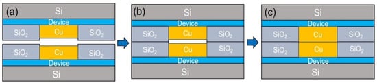
Figure 8.
Schematic of the ideal bonding mechanism of the Cu/SiO2 hybrid system. (a) Sides with Cu bumps in SiO2 via. The height of the Cu bump is slightly lower than the surrounding SiO2 layer. (b) Alignment and bonding of SiO2 to SiO2 at room temperature. (c) Heating to close the dishing gap and induce pressure in the Cu bump. The pressure was created due to the large CTE of the Cu. No external pressure is needed at the third stage.
However, on the other hand, the SiO2 layers are under tensile stress during the high temperature bonding process. When the Cu recess is too small, the expanding of Cu may apply high tensile stress in the oxide layer, causing a rupture of the SiO2 layers. When the recess of the Cu via is too much, the two Cu vias may not be able to contact each other and the bonding of Cu-Cu could not be accomplished. Therefore, the control of the Cu recess is critical in Cu/SiO2 hybrid bonding. The optimal height difference depends on the bonding temperature. The higher the bonding temperature is, the larger the height difference is.
Furthermore, low temperature Cu/SiO2 possesses the following advantages. Some devices, such as high bandwidth memories, prefer low temperature (<230 °C) hybrid bonding to prevent data retention errors. In addition, wafer warpage and thermal stress is lower at a low temperature, and delamination between the SiO2 layers and other film structures in the active device region could be avoided. Nevertheless, low temperature bonding is very challenging. Because the Cu will expand less at low temperatures. Therefore, the optimal height difference is smaller, which means recess control on the Cu vias is more difficult.
The maximum Cu recess could be estimated at a given bonding temperature. Typically, the height difference caused by CTE difference can be expressed as
where L0 is the thickness at room temperature in this study, ΔL is the height difference due to the mismatch between the thermal expansion of Cu and the oxide, Δα is the difference in CTE, and ΔT is temperature difference. In this work, we take the Cu/oxide layer to be 2 μm thick, and the bonding temperature is 200 °C. The estimated maximum recess for the Cu via is 4.3 nm. It means that when the Cu dishing is larger than 4.3 nm, the two Cu vias would not be able to touch each other when the temperature is increased to 200 °C. In this work, we control the Cu recess height to be 3 nm. Therefore, the Cu vias expand approximately 4.3 nm at 200 °C to contact with each other and provide suitable compressive stress for the Cu-Cu bonding.
ΔL = Δα L0 ΔT
ΔL = Δα L0 ΔT = (16.6 − 4.4) × 10−6 × 2000 nm × (200 − 25) = 4.3 nm
It is also crucial to produce a uniform Cu recess for good bonding. Otherwise, large voids may occur to weaken the mechanical, electrical, and thermal performance. As schematically shown in Figure 9a,b, when non-uniformity (dish shape) is generated after the CMP process and after the bonding of the oxide layers, only the periphery of the Cu vias can be well-bonded after the high temperature annealing (Figure 9c). Large voids or seams may remain after the bonding process. The voids may not be able to be eliminated, even after a long annealing time. For nt-Cu vias, uniform recesses were obtained due to their high hardness of 2.2 GPa, as illustrated in Figure 3a and Figure 4. Therefore, there are no large voids observed in the bonding interface, and thus the specific contact resistance is low.
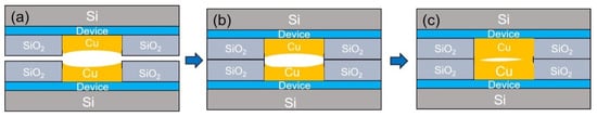
Figure 9.
Schematic of the bonding mechanism with non-uniform bonding surfaces in a Cu/SiO2 hybrid system. (a) Sides with Cu bumps in SiO2 via. The non-uniformity (dish shape) on Cu surface is generated after the CMP process (b) Alignment and bonding of SiO2 to SiO2 at room temperature with dishing Cu. (c) The periphery of the Cu vias can be well-bonded after high temperature annealing. No external pressure is needed at the third stage.
4. Conclusions
By adopting the highly <111>-oriented nt-Cu, we can fabricate nt-Cu/ SiO2 hybrid bonds at 200 °C with a very low specific contact resistance of 1.2 × 10⁻⁹ Ω·cm2, which is the lowest value reported in literature for Cu-Cu bonds fabricated below 200 °C. Excellent thermal and electrical stability was obtained up to 375 °C. The main reasons for the excellent electrical performance are that the <111>-oriented nt-Cu possesses high surface diffusivity and low oxidation rate, thus the nt-Cu vias can be bonded at a low temperature. More importantly, the nt-Cu possesses high hardness and thus the height and shape of the Cu recess can be well controlled by CMP to realize the low temperature Cu/SiO2 hybrid bonding. The mechanism of hybrid bonding is also discussed, and a mismatch in thermal expansion of Cu and SiO2 was utilized to produce compressive stress for the Cu-Cu bonding. The results indicate that the nt-Cu is suitable for low temperature Cu/SiO2 hybrid bonding.
Author Contributions
Conceptualization, J.-J.O., W.-L.C. and C.C.; Methodology, J.-J.O., W.-L.C. and C.C.; Software, J.-J.O.; Validation, W.-L.C., K.-N.T. and C.C.; Formal analysis, J.-J.O., W.-L.C., O.-H.L., C.-W.C., H.-H.C., C.-H.W., K.-C.S., S.-C.Y., D.-P.T., K.-N.T. and C.C.; Investigation, J.-J.O. and W.-L.C.; Resources, W.-L.C. and C.C.; Data curation, J.-J.O.; Writing—original draft preparation, J.-J.O. and W.-L.C.; Writing—review and editing, J.-J.O., W.-L.C., O.-H.L., C.-W.C., D.-P.T., K.-N.T. and C.C.; Supervision, C.C.; Project administration, C.C.; Funding acquisition, C.C. All authors have read and agreed to the published version of the manuscript.
Funding
This work was supported by the “Center for the Semiconductor Technology Research” of the Ministry of Education in Taiwan, the Ministry of Science and Technology, Taiwan, under Grant MOST 110-2634-F-009-027 and MOST 110-2221-E-A49-075-MY3, the Ministry of Economic Affairs (MOEA), Taiwan, R.O.C., and Semiconductor Research Corporation (SRC), USA.
Data Availability Statement
The data presented in this study are available on request from the corresponding author.
Acknowledgments
The authors would like to thank Chen-Ming Hu from Berkeley for helpful comments.
Conflicts of Interest
The authors declare no conflict of interest.
References
- Chen, M.-F.; Chen, F.-C.; Chiou, W.-C.; Yu, D.C.H. System on Integrated Chips (SoIC(TM) for 3D Heterogeneous Integration. In Proceedings of the 2019 IEEE 69th Electronic Components and Technology Conference (ECTC), Las Vegas, NV, USA, 28–31 May 2019; pp. 594–599. [Google Scholar] [CrossRef]
- Chen, Y.H.; Yang, C.A.; Kuo, C.C.; Chen, M.F.; Tung, C.H.; Chiou, W.C.; Yu, D. Ultra high density SoIC with sub-micron bond pitch. In Proceedings of the 2020 IEEE 70th Electronic Components and Technology Conference (ECTC), Orlando, FL, USA, 3–30 June 2020; pp. 576–581. [Google Scholar] [CrossRef]
- Tu, K.-N.; Chen, C.; Chen, H.-M. Electronic Packaging Science and Technology, 1st ed.; John Wiley & Sons: Hoboken, NJ, USA, 2022; pp. 19–57. [Google Scholar]
- Kagawa, Y.; Fujii, N.; Aoyagi, K.; Kobayashi, Y.; Nishi, S.; Todaka, N.; Hirayama, T. Novel stacked CMOS image sensor with advanced Cu2Cu hybrid bonding. In Proceedings of the 2016 IEEE International Electron Devices Meeting (IEDM), San Francisco, CA, USA, 3–7 December 2016; pp. 8–14. [Google Scholar] [CrossRef]
- Beyne, E.; Kim, S.W.; Peng, L.; Heylen, N.; De Messemaeker, J.; Okudur, O.O.; Beyer, G. Scalable, sub 2 μm pitch, Cu/SiCN to Cu/SiCN hybrid wafer-to-wafer bonding technology. In Proceedings of the 2017 IEEE International Electron Devices Meeting (IEDM), San Francisco, CA, USA, 2–6 December 2017; pp. 32–34. [Google Scholar] [CrossRef]
- Jourdon, J.; Lhostis, S.; Moreau, S.; Chossat, J.; Arnoux, M.; Sart, C.; Cheramy, S. Hybrid bonding for 3D stacked image sensors: Impact of pitch shrinkage on interconnect robustness. In Proceedings of the 2018 IEEE International Electron Devices Meeting (IEDM), San Francisco, CA, USA, 1–5 December 2018; pp. 7–13. [Google Scholar] [CrossRef]
- Chou, T.C.; Yang, K.M.; Li, J.C.; Yu, T.Y.; Chung, Y.T.; Ko, C.T.; Chen, K.N. Non-planarization Cu-Cu direct bonding and gang bonding with low temperature and short duration in ambient atmosphere. In Proceedings of the 2019 IEEE International Electron Devices Meeting (IEDM), San Francisco, CA, USA, 7–11 December 2019; pp. 5–15. [Google Scholar] [CrossRef]
- Kim, S.W.; Fodor, F.; Heylen, N.; Iacovo, S.; De Vos, J.; Miller, A.; Beyne, E. Novel Cu/SiCN surface topography control for 1 μm pitch hybrid wafer-to-wafer bonding. In Proceedings of the 2020 IEEE 70th Electronic Components and Technology Conference (ECTC), Orlando, FL, USA, 3–30 June 2020; pp. 216–222. [Google Scholar] [CrossRef]
- Lu, L.; Shen, Y.; Chen, X.; Qian, L.; Lu, K. Ultrahigh strength and high electrical conductivity in copper. Science 2004, 304, 422–426. [Google Scholar] [CrossRef] [PubMed] [Green Version]
- Tseng, C.H.; Tu, K.N.; Chen, C. Comparison of oxidation in uni-directionally and randomly oriented Cu films for low temperature Cu-to-Cu direct bonding. Sci. Rep. 2018, 8, 10671. [Google Scholar] [CrossRef] [PubMed]
- Chen, K.C.; Wu, W.W.; Liao, C.N.; Chen, L.J.; Tu, K.N. Observation of atomic diffusion at twin-modified grain boundaries in copper. Science 2008, 321, 1066–1069. [Google Scholar] [CrossRef] [PubMed] [Green Version]
- Hsiao, H.Y.; Liu, C.M.; Lin, H.W.; Liu, T.C.; Lu, C.L.; Huang, Y.S.; Tu, K.N. Unidirectional growth of microbumps on (111)-oriented and nanotwinned copper. Science 2012, 336, 1007–1010. [Google Scholar] [CrossRef] [PubMed] [Green Version]
- Liu, C.M.; Lin, H.W.; Huang, Y.S.; Chu, Y.C.; Chen, C.; Lyu, D.R.; Tu, K.N. Low-temperature direct copper-to-copper bonding enabled by creep on (111) surfaces of nanotwinned Cu. Sci. Rep. 2015, 5, 9734. [Google Scholar] [CrossRef] [PubMed] [Green Version]
- Liu, C.M.; Lin, H.W.; Chu, Y.C.; Chen, C.; Lyu, D.R.; Chen, K.N.; Tu, K.N. Low-temperature direct copper-to-copper bonding enabled by creep on highly (111)-oriented Cu surfaces. Scr. Mater. 2014, 78, 65–68. [Google Scholar] [CrossRef]
- Shie, K.C.; Gusak, A.M.; Tu, K.N.; Chen, C. A kinetic model of copper-to-copper direct bonding under thermal compression. J. Mater. Res. Technol. 2012, 15, 2332–2344. [Google Scholar] [CrossRef]
- Liu, H.C.; Gusak, A.M.; Tu, K.N.; Chen, C. Interfacial void ripening in Cu-Cu joints. Mater. Charact. 2021, 181, 111459. [Google Scholar] [CrossRef]
- Chiu, W.L.; Lee, O.H.; Chiang, C.W.; Chang, H.H. Low Temperature Wafer-To-Wafer Hybrid Bonding by Nanotwinned Copper. In Proceedings of the 2021 IEEE 71st Electronic Components and Technology Conference (ECTC), San Diego, CA, USA, 1 June–4 July 2021; pp. 365–370. [Google Scholar] [CrossRef]
- Shie, K.C.; Hsu, P.N.; Li, Y.J.; Tu, K.N.; Lin, B.T.H.; Chang, C.C.; Chen, C. Electromigration and temperature cycling tests of Cu-Cu joints fabricated by instant copper direct bonding. In Proceedings of the 2021 IEEE 71st Electronic Components and Technology Conference (ECTC), San Diego, CA, USA, 1 June–4 July 2021; pp. 995–1000. [Google Scholar] [CrossRef]
- Tran, D.P.; Chen, K.J.; Tu, K.N.; Chen, C.; Chen, Y.T.; Chung, S. Electrodeposition of slanted nanotwinned Cu foils with high strength and ductility. Electrochim. Acta 2021, 389, 138640. [Google Scholar] [CrossRef]
- Ong, J.J.; Tran, D.P.; Yang, S.C.; Shie, K.C.; Chen, C. Shearing characteristics of Cu-Cu joints fabricated by two-step process using highly <111>-oriented nanotwinned Cu. Metals 2021, 11, 1864. [Google Scholar] [CrossRef]
- Cheng, H.Y.; Tran, D.P.; Tu, K.N.; Chen, C. Effect of deposition temperature on mechanical properties of nanotwinned Cu fabricated by rotary electroplating. Mater. Sci. Eng. A 2021, 811, 141065. [Google Scholar] [CrossRef]
- Li, Y.J.; Tu, K.N.; Chen, C. Tensile properties and thermal stability of unidirectionally <111>-oriented nanotwinned and <110>-oriented microtwinned copper. Materials 2020, 13, 1211. [Google Scholar] [CrossRef] [Green Version]
- Tseng, I.H.; Hsu, P.N.; Lu, T.L.; Tu, K.N.; Chen, C. Electromigration failure mechanisms of <111>-oriented nanotwinned Cu redistribution lines with polyimide capping. Results Phys. 2021, 24, 104154. [Google Scholar] [CrossRef]
- Chen, K.N.; Fan, A.; Tan, C.S.; Reif, R. Contact resistance measurement of bonded copper interconnects for three-dimensional integration technology. IEEE Electron. Device Lett. 2004, 25, 10–12. [Google Scholar] [CrossRef]
- Gueguen, P.; Di Cioccio, L.; Morfouli, P.; Zussy, M.; Dechamp, J.; Bally, L.; Clavelier, L. Copper direct bonding: An innovative 3D interconnect. In Proceedings of the 2010 Proceedings 60th Electronic Components and Technology Conference (ECTC), Las Vegas, NV, USA, 1–4 June 2010; pp. 878–883. [Google Scholar] [CrossRef]
- Tan, C.S.; Peng, L.; Li, H.Y.; Lim, D.F.; Gao, S. Wafer-on-wafer stacking by bumpless Cu–Cu bonding and its electrical characteristics. IEEE Electron. Device Lett. 2011, 32, 943–945. [Google Scholar] [CrossRef]
- Peng, L.; Li, H.Y.; Lim, D.F.; Lo, G.Q.; Kwong, D.L.; Tan, C.S. High density bump-less Cu-Cu bonding with enhanced quality achieved by pre-bonding temporary passivation for 3D wafer stacking. In Proceedings of the 2011 International Symposium on VLSI Technology, Systems and Applications, Hsinchu, Taiwan, 25–27 April 2011; pp. 1–2. [Google Scholar] [CrossRef]
- Shigetou, A.; Itoh, T.; Sawada, K.; Suga, T. Bumpless interconnect of 6-µm-pitch Cu electrodes at room temperature. IEEE Trans. Adv. Packag. 2008, 31, 473–478. [Google Scholar] [CrossRef]
- Beilliard, Y.; Moreau, S.; Di Cioccio, L.; Coudrain, P.; Romano, G.; Nowodzinski, A.; Signamarcheix, T. Advances toward reliable high density Cu-Cu interconnects by Cu-SiO2 direct hybrid bonding. In Proceedings of the 2014 International 3D Systems Integration Conference (3DIC), Kinsdale, Ireland, 1–3 December 2014; pp. 1–8. [Google Scholar] [CrossRef]
- Jansen, F.; Machonkin, M.A.; Palmieri, N.; Kuhman, D. Thermal expansion and elastic properties of plasma-deposited amorphous silicon and silicon oxide films. Appl. Phys. Lett. 1987, 50, 1059–1061. [Google Scholar] [CrossRef]
Publisher’s Note: MDPI stays neutral with regard to jurisdictional claims in published maps and institutional affiliations. |
© 2022 by the authors. Licensee MDPI, Basel, Switzerland. This article is an open access article distributed under the terms and conditions of the Creative Commons Attribution (CC BY) license (https://creativecommons.org/licenses/by/4.0/).