
Structural and Insulating Behaviour of High-Permittivity Binary Oxide Thin Films for Silicon Carbide and Gallium Nitride Electronic Devices


 ,
,  ,
, 
Abstract
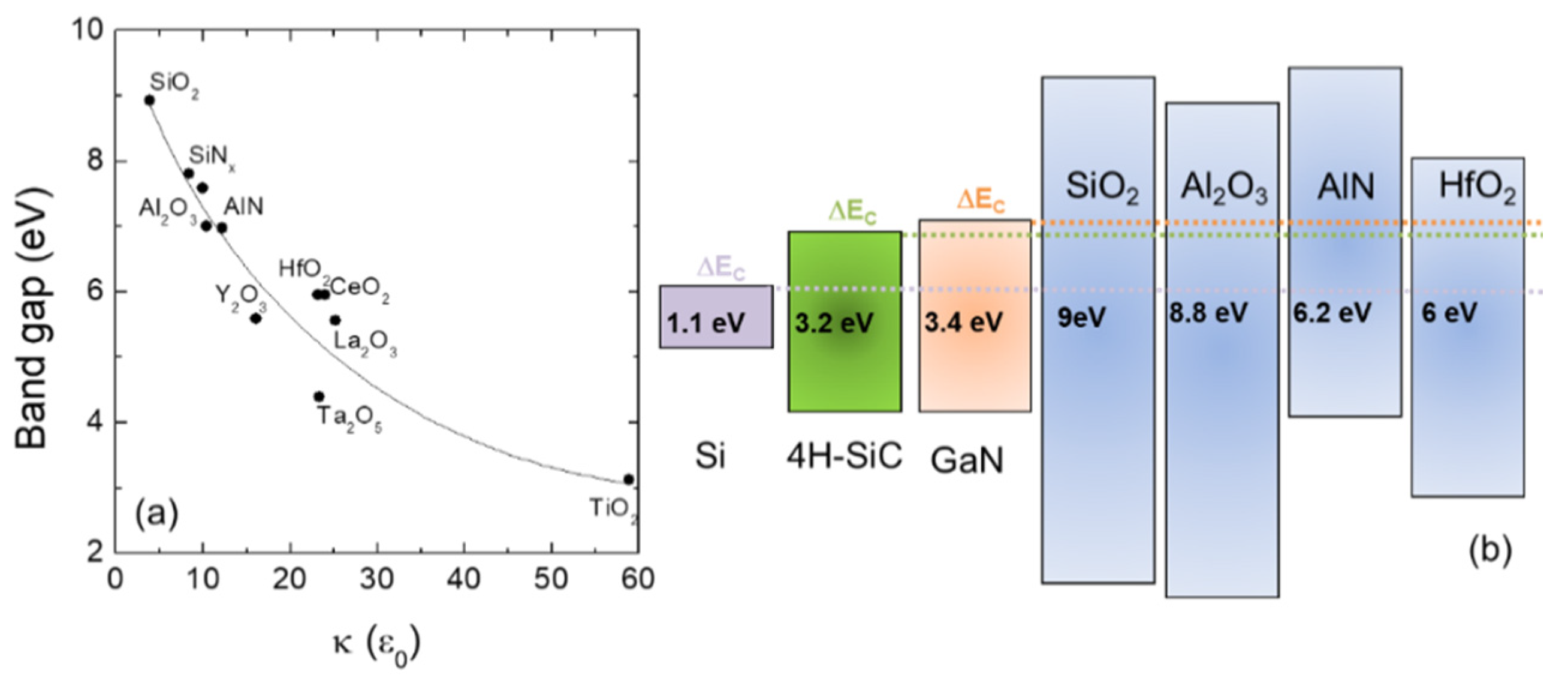
1. Introduction
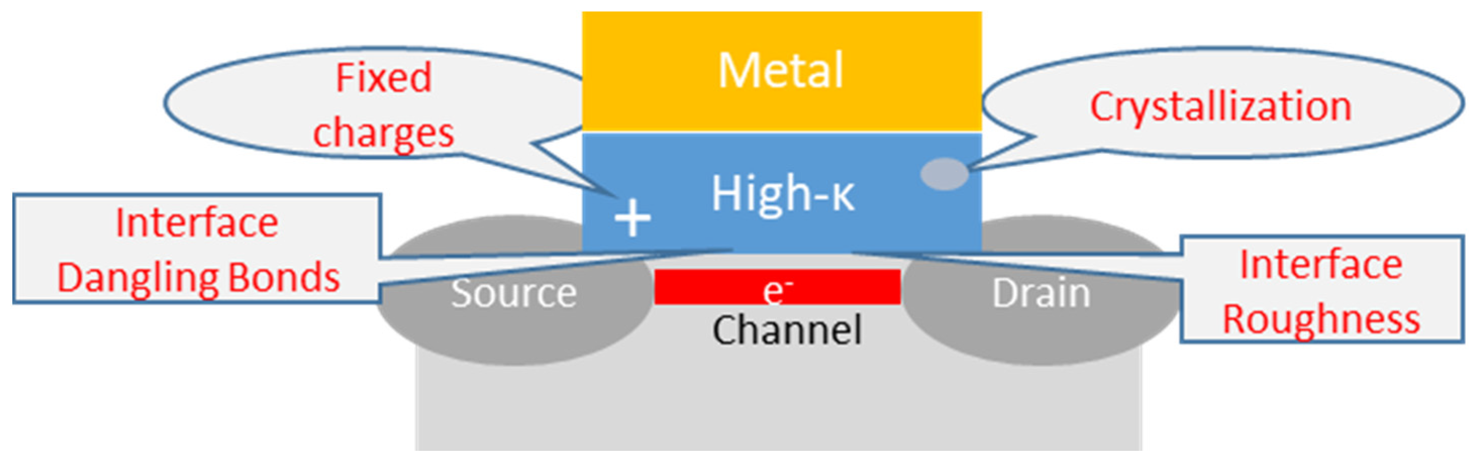
2. Amorphous High-κ Oxides on WBG Semiconductors
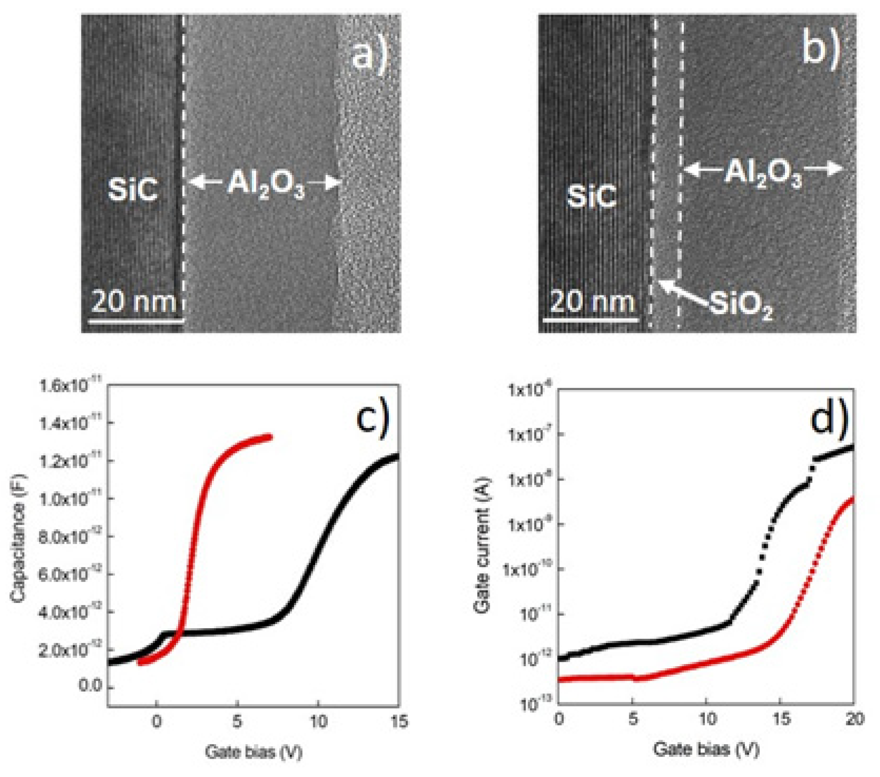
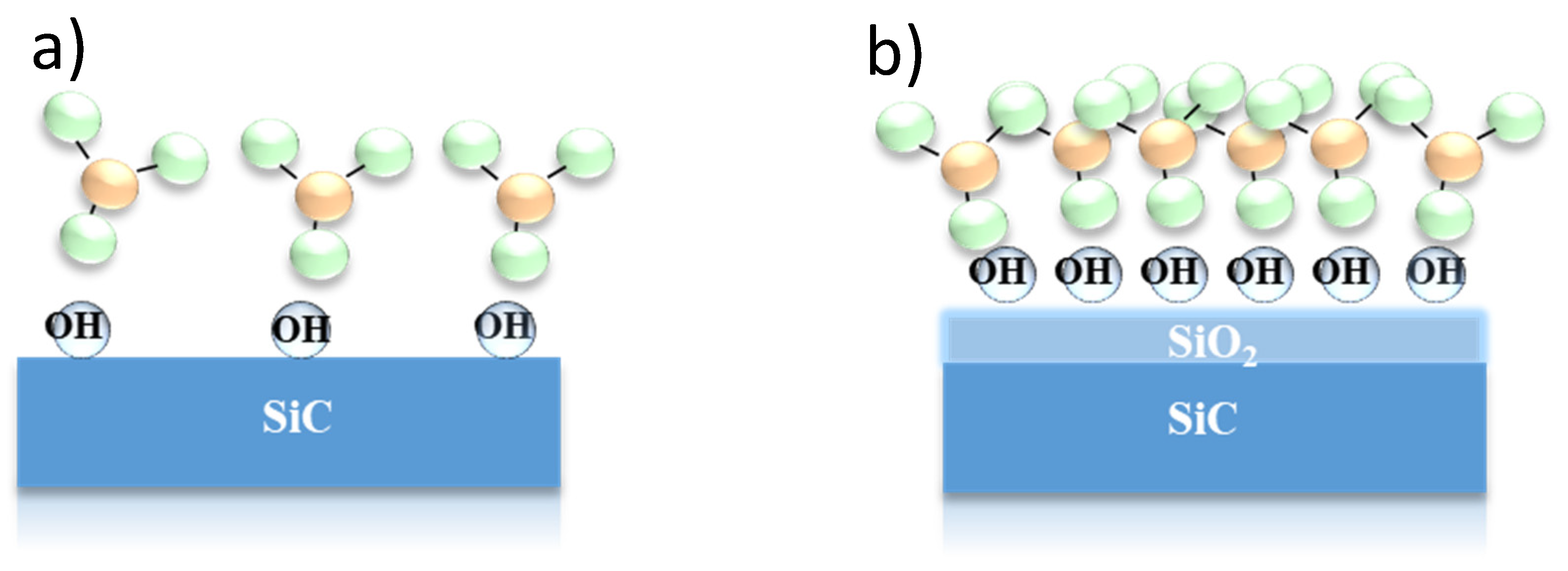
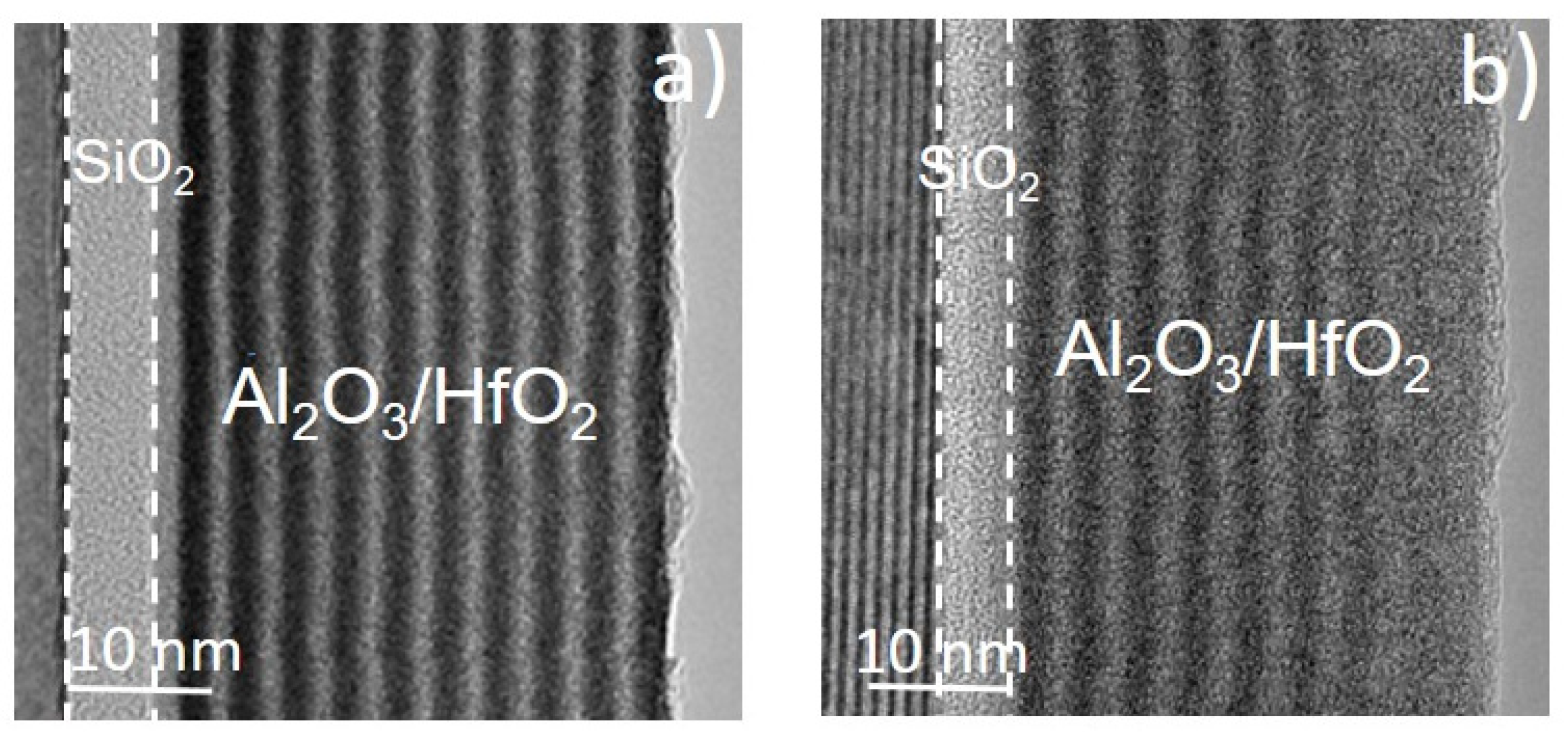
2.1. Growth of Amorphous High-κ Oxides on SiC
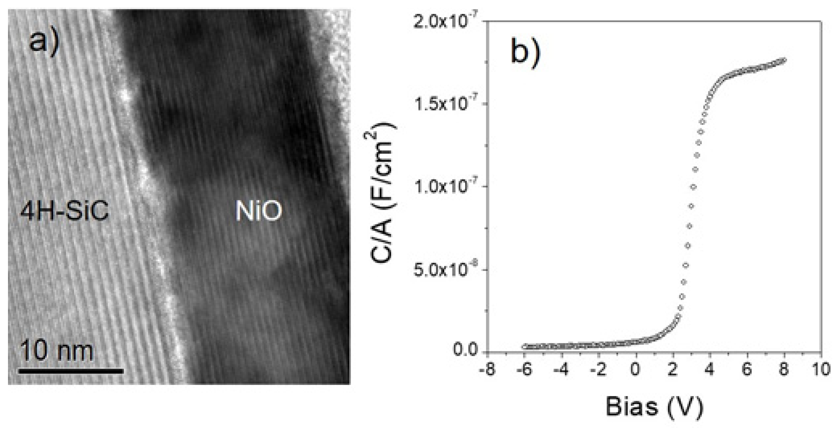
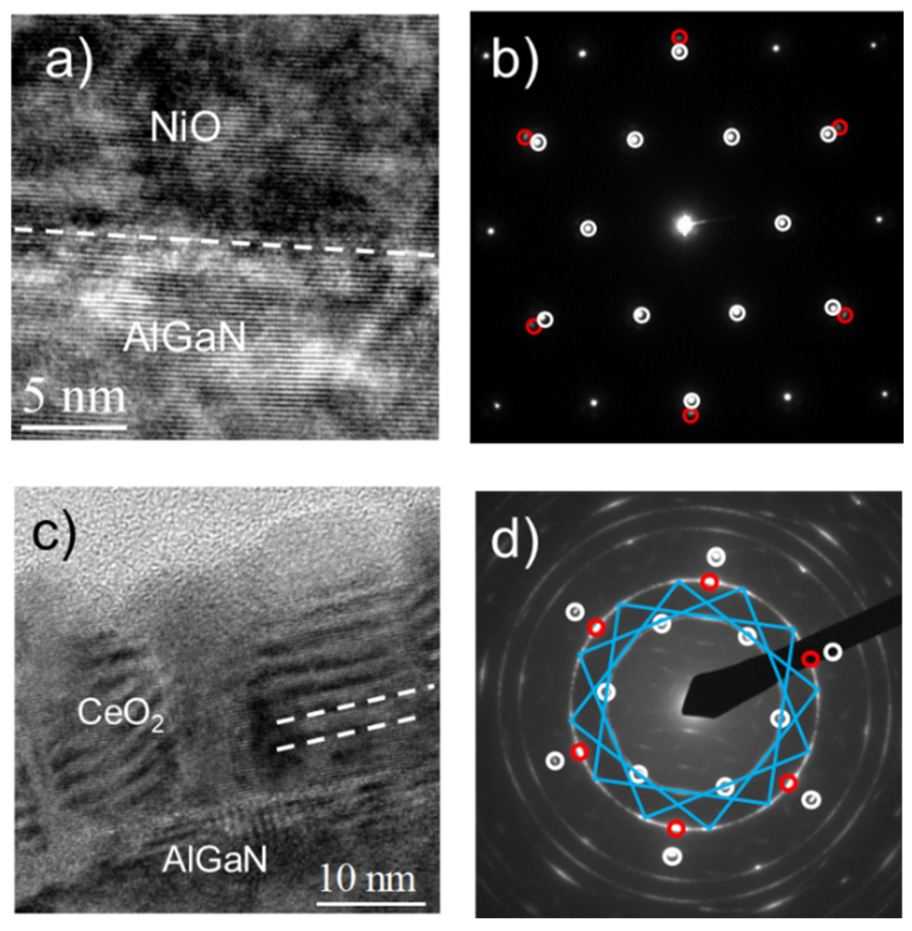
2.2. Growth of Amorphous High-κ Oxides on GaN-based Materials
3. Epitaxial Growth of High-κ Oxides on WBG Semiconductors
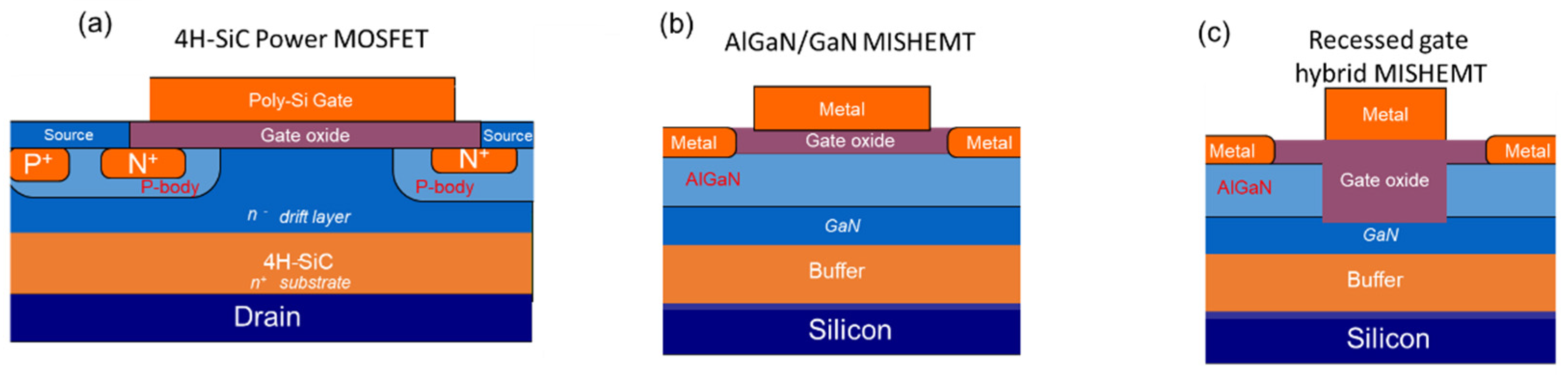
4. Application of High-κ Oxides as Gate Dielectrics in SiC and GaN Transistors
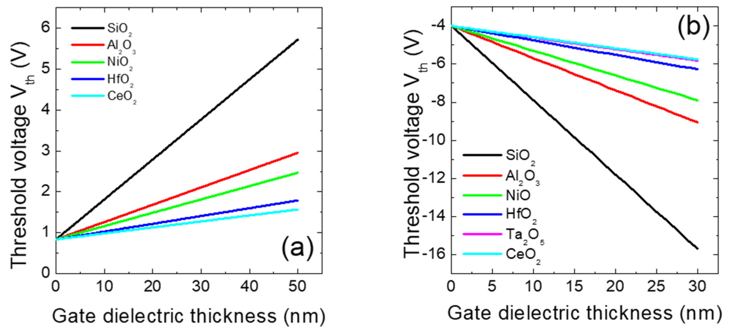
4.1. Binary High-κ Oxides in 4H-SiC MOSFETs
4.2. Binary High-κ Oxides for GaN-based MISHEMTs

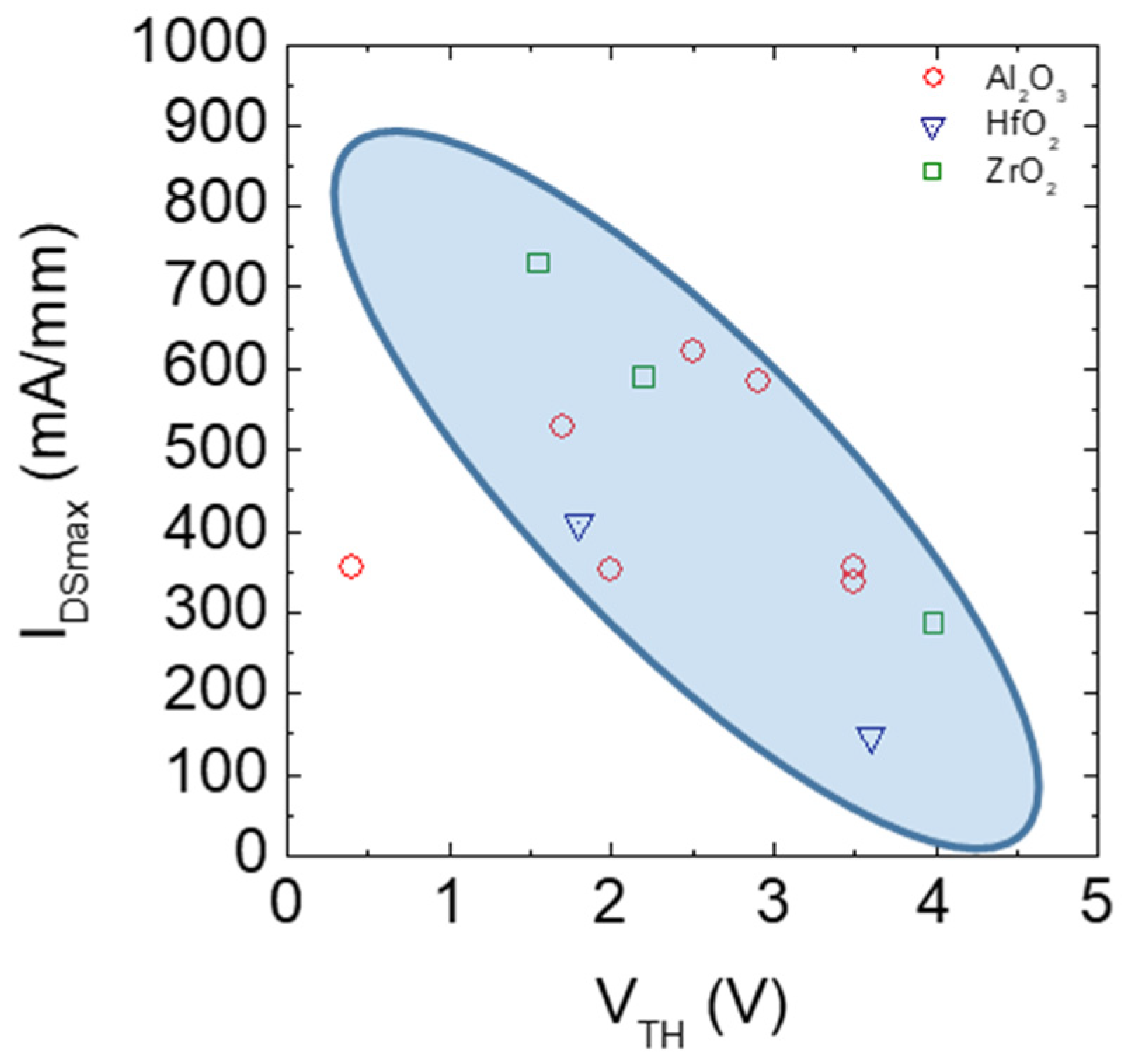
| Dielectric | Thickness (nm) | VTH (V) | Mobility (cm2/Vs) | RON (Ωmm or mΩcm2) | IDSS (mA/mm) | Ref. |
|---|---|---|---|---|---|---|
| Al2O3 | 30 | 2 | 225 | 7.8 Ωmm | 353 | [141] |
| 38 | 3.5 | 55 | 27 Ωmm | 336 | [142] | |
| 10 | 1.7 | 251 | 9.8 Ωmm | 528 | [143] | |
| 20 | 2.9 | 148 | 7.2 Ωmm | 585 | [144] | |
| 30 | 3.5 | 170 | 9.5 Ωmm | 355 | [145] | |
| 30 | 2.5 | 192 | 9.6 Ωmm | 620 | [146] | |
| 23 | 0.4 | 396 | 13.3 Ωmm | 356 | [147] | |
| HfO2 | 30 | 1.8 (partial recessed) | 876 | 5.2 mΩcm2 | 411 | [150] |
| 3.6 (total recessed) | 118 | 12.2 mΩcm2 | 146 | |||
| HfSiOx | 15 | 2.2 | 520 | 10.1 Ωmm | 519 | [154] |
| LaHfOx | 8 | 0.35 | 9.4 Ωmm | 648 | [144] | |
| ZrO2 | 20 | 3.99 | 210 | 24 Ωmm | 286 | [151] |
| 23 | 2.2 (partial recessed) | 850 | 9.2 Ωmm | 590 | [152] | |
| 16 | 1.55 (partial recessed) | 1450 | 7.1 Ωmm | 730 | [153] |
5. Conclusions
Author Contributions
Funding
Data Availability Statement
Acknowledgments
Conflicts of Interest
References
- Bose, K.B. Power Electronics–An Emerging Technology. IEEE Trans. Ind. Electr. 1989, 36, 403–412. [Google Scholar] [CrossRef]
- Brunco, D.P.; De Jaeger, B.; Eneman, G.; Mitard, J.; Hellings, G.; Satta, A.; Terzieva, V.; Souriau, L.; Leys, F.E.; Pourtois, G.; et al. Germanium MOSFET Devices: Advances in Materials Understanding, Process Development, and Electrical Performance. J. Electrochem. Soc. 2008, 155, H552–H561. [Google Scholar] [CrossRef]
- Wong, H.-S.P. Beyond the conventional transistor. IBM J. Res. Dev. 2002, 46, 133–168. [Google Scholar] [CrossRef]
- Ostling, M.; Ghandi, R.; Zetterling, C.-M. SiC power devices Present status, applications and future perspective. In Proceedings of the 2011 IEEE 23rd International Symposium on Power Semiconductor Devices and ICs, San Diego, CA, USA, 23–26 May 2011; IEEE: Piscataway, NJ, USA, 2011; pp. 10–15. [Google Scholar]
- Roccaforte, F.; Fiorenza, P.; Greco, G.; Nigro, R.L.; Giannazzo, F.; Iucolano, F.; Saggio, M. Emerging trends in wide band gap semiconductors (SiC and GaN) technology for power devices. Microelectron. Eng. 2018, 187–188, 66–77. [Google Scholar] [CrossRef]
- Chen, K.J.; Haberlen, O.; Lidow, A.; Tsai, C.L.; Ueda, T.; Uemoto, Y.; Wu, Y. GaN-on-Si Power Technology: Devices and Applications. IEEE Trans. Electron Devices 2017, 64, 779–795. [Google Scholar] [CrossRef]
- Roccaforte, F.; Fiorenza, P.; Nigro, R.L.; Giannazzo, F.; Greco, G. Physics and technology of gallium nitride materials for power electronics. Riv. Nuovo Cim. 2018, 41, 625–681. [Google Scholar]
- Kimoto, T.; Cooper, J. Fundamentals of Silicon Carbide Technology: Growth, Characterization, Devices and Applications; JohnWiley & Sons: Hoboken, NJ, USA, 2014. [Google Scholar]
- Roccaforte, F.; Leszczynski, M. Introduction to Gallium Nitride Properties and Applications. In Nitride Semiconductor Technology: Power Electronics and Optoelectronic Devices, 1st ed.; Roccaforte, F., Leszczyński, M., Eds.; Wiley-VCH Verlag: Weinheim, Germany; GmbH & Co. KGaA: Lippstadt, Germany, 2020; pp. 1–39. [Google Scholar]
- Saggio, M.; Guarnera, A.; Zanetti, E.; Rascunà, S.; Frazzetto, A.; Salinas, D.; Giannazzo, F.; Fiorenza, P.; Roccaforte, F. Industrial Approach for Next Generation of Power Devices Based on 4H-SiC. Mater. Sci. Forum 2015, 821–823, 660–666. [Google Scholar] [CrossRef]
- Arulkumaran, S.; Egawa, T.; Ishikawa, H.; Jimbo, T.; Sano, Y. Surface passivation effects on AlGaN/GaN high-electron-mobility transistors with SiO2, Si3N4, and silicon oxynitride. Appl. Phys. Lett. 2004, 84, 613–615. [Google Scholar] [CrossRef]
- Nakano, Y.; Jimbo, T. Interface properties of SiO2/n-GaN metal–insulator–semiconductor structures. Appl. Phys. Lett. 2002, 80, 4756–4758. [Google Scholar] [CrossRef]
- Cook, T.E.; Fulton, C.C.; Mecouch, W.; Davis, R.; Lucovsky, G.; Nemanich, R.J. Band offset measurements of the Si3N4/GaN (0001) interface. J. Appl. Phys. 2003, 94, 3949–3954. [Google Scholar] [CrossRef]
- Placidi, M.; Constant, A.; Fontserè, A.; Pausas, E.; Cortes, I.; Cordier, Y.; Mestres, N.; Pérez, R.; Zabala, M.; Millán, J.; et al. Deposited Thin SiO2 for Gate Oxide on n-Type and p-Type GaN. J. Electrochem. Soc. 2010, 157, H1008–H1013. [Google Scholar] [CrossRef]
- Schlom, D.G.; Guha, S.; Datta, S. Gate Oxides Beyond SiO2. MRS Bull. 2008, 33, 1017–1025. [Google Scholar] [CrossRef]
- Kingon, A.I.; Maria, J.-P.; Streiffer, S.K. Alternative dielectrics to silicon dioxide for memory and logic devices. Nature 2000, 406, 1032–1038. [Google Scholar] [CrossRef] [PubMed]
- Wallace, R.M.; Wilk, G.D. High-k dielectric material for microelectronics. Critic. Rev. Solid State Mater. Sci. 2003, 28, 231–285. [Google Scholar] [CrossRef]
- Wilk, G.D.; Wallace, R.; Anthony, J.M. High-κ gate dielectrics: Current status and materials properties considerations. J. Appl. Phys. 2001, 89, 5243–5275. [Google Scholar] [CrossRef]
- Roccaforte, F.; Fiorenza, P.; Greco, G.; Vivona, M.; Nigro, R.L.; Giannazzo, F.; Patti, A.; Saggio, M. Recent advances on dielectrics technology for SiC and GaN power devices. Appl. Surf. Sci. 2014, 301, 9–18. [Google Scholar] [CrossRef]
- Gaskins, J.T.; Hopkins, P.E.; Merrill, D.R.; Bauers, S.R.; Hadland, E.; Johnson, D.C.; Koh, D.; Yum, J.H.; Banerjee, S.; Nordell, B.J.; et al. Review—Investigation and Review of the Thermal, Mechanical, Electrical, Optical, and Structural Properties of Atomic Layer Deposited High-kDielectrics: Beryllium Oxide, Aluminum Oxide, Hafnium Oxide, and Aluminum Nitride. ECS J. Solid State Sci. Technol. 2017, 6, N189–N208. [Google Scholar] [CrossRef]
- Ye, P.D.; Yang, B.; Ng, K.K.; Bude, J.; Wilk, G.D.; Halder, S.; Hwang, J.C.M. GaN metal-oxide-semiconductor high-electron-mobility-transistor with atomic layer deposited Al2O3 as gate dielectric. Appl. Phys. Lett. 2005, 86, 63501. [Google Scholar] [CrossRef]
- Yue, Y.; Hao, Y.; Zhang, J.; Ni, J.; Mao, W.; Feng, Q.; Liu, L. AlGaN/GaN MOS-HEMT with HfO2 Dielectric and Al2O3 Interfacial Passivation Layer Grown by Atomic Layer Deposition. IEEE Electron Device Lett. 2008, 29, 838–840. [Google Scholar] [CrossRef]
- Roccaforte, F.; Greco, G.; Fiorenza, P.; Raineri, V.; Malandrino, G.; Nigro, R.L. Epitaxial NiO gate dielectric on AlGaN/GaN heterostructures. Appl. Phys. Lett. 2012, 100, 63511. [Google Scholar] [CrossRef]
- Fiorenza, P.; Greco, G.; Giannazzo, F.; Nigro, R.L.; Roccaforte, F. Poole-Frenkel emission in epitaxial nickel oxide on AlGaN/GaN heterostructures. Appl. Phys. Lett. 2012, 101, 172901. [Google Scholar] [CrossRef]
- Fiorenza, P.; Greco, G.; Fisichella, G.; Roccaforte, F.; Malandrino, G.; Nigro, R.L. High permittivity cerium oxide thin films on AlGaN/GaN heterostructures. Appl. Phys. Lett. 2013, 103, 112905. [Google Scholar] [CrossRef]
- Milanov, A.P.; Xu, K.; Cwik, S.; Parala, H.; Arcos, T.D.L.; Becker, H.-W.; Rogalla, D.; Cross, R.; Paul, S.; Devi, A. Sc2O3, Er2O3, and Y2O3 thin films by MOCVD from volatile guanidinate class of rare-earth precursors. Dalton Trans. 2012, 41, 13936–13947. [Google Scholar] [CrossRef] [PubMed]
- Chen, J.-J.; Gila, B.P.; Hlad, M.; Gerger, A.; Ren, F.; Abernathy, C.R.; Pearton, S. Band offsets in the Sc2O3/GaN heterojunction system. Appl. Phys. Lett. 2006, 88, 142115. [Google Scholar] [CrossRef]
- Prokofiev, A.; Shelykh, A.; Melekh, B. Periodicity in the band gap variation of Ln2X3 (X = O, S, Se) in the lanthanide series. J. Alloy. Compd. 1996, 242, 41–44. [Google Scholar] [CrossRef]
- Fanciulli, M.; Scarel, G. Rare Earth Oxide Thin Films; Springer: Berlin/Heidelberg, Germany, 2007. [Google Scholar]
- Fiedler, A.; Schewski, R.; Galazka, Z.; Irmscher, K. Static Dielectric Constant of β-Ga2O3 Perpendicular to the Principal Planes (100), (010), and (001). ECS J. Solid State Sci. Technol. 2019, 8, Q3083–Q3085. [Google Scholar] [CrossRef]
- Kääriäinen, T.; Cameron, D.; Kääriäinen, M.L.; Sherman, A. Atomic Layer Deposition, Principles Characteristics and Nanotechnolody Applications; Scrivener, M., Carmical, P., Eds.; John Wiley & Sons: Hoboken, NJ, USA, 2013. [Google Scholar]
- Ahvenniemi, E.; Akbashev, A.R.; Ali, S.; Bechelany, M.; Berdova, M.; Boyadjiev, S.; Cameron, D.C.; Chen, R.; Chubarov, M.; Cremers, V.; et al. Review Article: Recommended reading list of early publications on atomic layer deposition—Outcome of the Virtual Project on the History of ALD. J. Vac. Sci. Technol. A Vac. Surf. Film. 2017, 35, 10801. [Google Scholar] [CrossRef]
- Shukla, M.; Dutta, G.; Mannam, R.; DasGupta, N. Electrical properties of reactive-ion-sputtered Al2O3 on 4H-SiC. Thin Solid Film. 2016, 607, 1–6. [Google Scholar] [CrossRef]
- Paskaleva, A.; Ciechonski, R.R.; Syväjärvi, M.; Atanassova, E.; Yakimova, R. Electrical behavior of 4H-SiC metal-oxide-semiconductor structures with Al2O3 as gate dielectric. J. Appl. Phys. 2005, 97, 124507. [Google Scholar] [CrossRef]
- Fiorenza, P.; Vivona, M.; Di Franco, S.; Smecca, E.; Sanzaro, S.; Alberti, A.; Saggio, M.; Roccaforte, F. Properties of Al2O3 thin films deposited on 4H-SiC by reactive ion sputtering. Mater. Sci. Semicond. Process. 2019, 93, 290–294. [Google Scholar] [CrossRef]
- Khosa, R.Y.; Thorsteinsson, E.B.; Winters, M.; Rorsman, N.; Karhu, R.; Hassan, J.U.; Sveinbjörnsson, E.Ö. Electrical characterization of amorphous Al2O3 dielectric films on n-type 4H-SiC. AIP Adv. 2018, 8, 25304. [Google Scholar] [CrossRef]
- Wolborski, M.; Bakowski, M.; Ortiz, A.; Pore, V.; Schöner, A.; Ritala, M.; Leskelä, M.; Hallén, A. Characterisation of the Al2O3 films deposited by ultrasonic spray pyrolysis and atomic layer deposition methods for passivation of 4H–SiC devices. Microelectron. Reliab. 2006, 46, 743–755. [Google Scholar] [CrossRef]
- Huang, S.-W.; Hwu, J.-G. Ultrathin Aluminum Oxide Gate Dielectric on N-Type 4H-SiC Prepared by Low Thermal Budget Nitric Acid Oxidation. IEEE Trans. Electron Devices 2004, 51, 1877–1882. [Google Scholar] [CrossRef]
- Schilirò, E.; Nigro, R.L.; Fiorenza, P.; Roccaforte, F. Negative charge trapping effects in Al2O3 films grown by atomic layer deposition onto thermally oxidized 4H-SiC. AIP Adv. 2016, 6, 75021. [Google Scholar] [CrossRef]
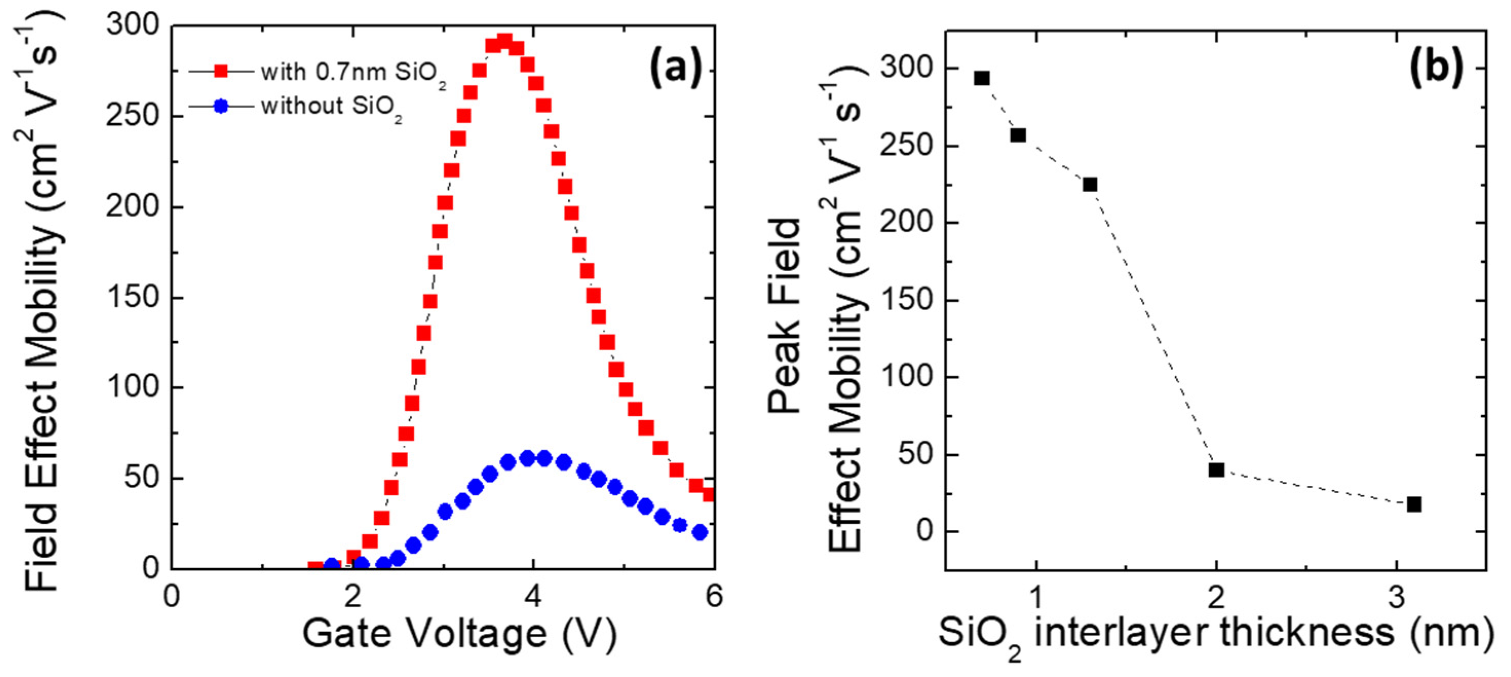
- Schilirò, E.; Fiorenza, P.; Di Franco, S.; Bongiorno, C.; Saggio, M.; Roccaforte, F.; Nigro, R.L. Effect of SiO2 interlayer on the properties of Al2O3 thin films grown by plasma enhanced atomic layer deposition on 4H-SiC substrates. Phys. Status Solidi 2016, 214, 1600365. [Google Scholar] [CrossRef]
- Tanner, C.M.; Perng, Y.-C.; Frewin, C.L.; Saddow, S.E.; Chang, J.P. Electrical performance of Al2O3 gate dielectric films deposited by atomic layer deposition on 4H-SiC. Appl. Phys. Lett. 2007, 91, 203510. [Google Scholar] [CrossRef]
- Avice, M.; Grossner, U.; Pintilie, I.; Svensson, B.G.; Servidori, M.; Nipoti, R.; Nilsen, O.; Fjellvåg, H. Electrical properties of Al2O3/4H-SiC structures grown by atomic layer chemical vapor deposition. J. Appl. Phys. 2007, 102, 54513. [Google Scholar] [CrossRef]
- Lichtenwalner, D.J.; Misra, V.; Dhar, S.; Ryu, S.-H.; Agarwal, A. High-mobility enhancement-mode 4H-SiC lateral field-effect transistors utilizing atomic layer deposited Al2O3 gate dielectric. Appl. Phys. Lett. 2009, 95, 152113. [Google Scholar] [CrossRef]
- Cheong, K.Y.; Moon, J.H.; Kim, H.J.; Bahng, W.; Kim, N.-K. Analysis of current conduction mechanisms in atomic-layer-deposited Al2O3 gate on 4H silicon carbide. Appl. Phys. Lett. 2007, 90, 162113. [Google Scholar] [CrossRef]
- Kern, W.; Puotinen, D.P. Cleaning Solutions Based on Hydrogen Peroxide for use in Silicon Semiconductor Technology. RCA Rev. 1970, 31, 187. [Google Scholar]
- Suvanam, S.S.; Usman, M.; Martin, D.; Yazdi, M.G.; Linnarsson, M.K.; Tempez, A.; Gotelid, M.; Hallen, A. Improved interface and electrical properties of atomic layer deposited Al2O3/4H-SiC. Appl. Surf. Sci. 2018, 433, 108–115. [Google Scholar] [CrossRef]
- Yoshioka, H.; Yamazaki, M.; Harada, S. Reduction of interface states by hydrogen treatment at the aluminum oxide/4H-SiC Si-face interface. AIP Adv. 2016, 6, 105206. [Google Scholar] [CrossRef]
- Plummer, J.D.; Deal, M.; Griffin, P.D. Silicon VLSI Technology: Fundamentals, Practice and Modelling, 1st ed.; Prentice Hall: Hoboken, NJ, USA, 2000. [Google Scholar]
- Heo, S.C.; Lim, D.; Jung, W.S.; Choi, R.; Yu, H.-Y.; Choi, C. Remote plasma atomic layer deposited Al2O3 4H SiC MOS capacitor with remote H2 plasma passivation and post metallization annealing. Microelectron. Eng. 2015, 147, 239–243. [Google Scholar] [CrossRef]
- Wang, Y.-Y.; Shen, H.-J.; Bai, Y.; Tang, Y.-D.; Liu, K.-A.; Li, C.-Z.; Liu, X.-Y. Influences of high-temperature annealing on atomic layer deposited Al2O3/4H-SiC. Chin. Phys. B 2013, 22, 78102. [Google Scholar] [CrossRef]
- Idris, M.I.; Wright, N.G.; Horsfall, A.B. Effect of Post Oxide Annealing on the Electrical and Interface 4H-SiC/Al2O3 MOS Capacitors. Mater. Sci. Forum 2018, 924, 486–489. [Google Scholar] [CrossRef]
- Linnarsson, M.K.; Hallén, A.; Khartsev, S.; Suvanam, S.S.; Usman, M. Interface between Al2O3 and 4H-SiC investigated by time-of-flight medium energy ion scattering. J. Phys. D Appl. Phys. 2017, 50, 495111. [Google Scholar] [CrossRef]
- Liu, X.-Y.; Wang, Y.-Y.; Peng, Z.-Y.; Li, C.-Z.; Wu, J.; Bai, Y.; Tang, Y.-D.; Liu, K.-A.; Shen, H.-J. Charge trapping behavior and its origin in Al2O3/SiC MIS system. Chin. Phys. B 2015, 24, 87304. [Google Scholar] [CrossRef]
- Usman, M.; Suvanam, S.S.; Yazdi, M.G.; Göthelid, M.; Sultan, M.; Hallén, A. Stoichiometry of the ALD-Al2O3/4H–SiC interface by synchrotron-based XPS. J. Phys. D Appl. Phys. 2016, 49, 255308. [Google Scholar] [CrossRef]
- Usman, M.; Suvanam, S.S.; Linnarsson, M.; Hallén, A. Improving the quality of Al2O3/4H-SiC interface for device applications. Mater. Sci. Semicond. Process. 2018, 81, 118–121. [Google Scholar] [CrossRef]
- Cheong, K.Y.; Moon, J.H.; Kim, H.J.; Bahng, W.; Kim, N.-K. Current conduction mechanisms in atomic-layer-deposited HfO2/nitrided SiO2 stacked gate on 4H silicon carbide. J. Appl. Phys. 2008, 103, 84113. [Google Scholar] [CrossRef]
- Cheong, K.Y.; Moon, J.H.; Park, T.J.; Kim, J.H.; Hwang, C.S.; Kim, H.J.; Bahng, W.; Kim, N.-K. Improved Electronic Performance of HfO2/SiO2 Stacking Gate Dielectric on 4H SiC. IEEE Trans. Electron Devices 2007, 54, 3409–3413. [Google Scholar] [CrossRef]
- Afanas’Ev, V.V.; Stesmans, A.; Chen, F.; Campbell, S.A.; Smith, R. HfO2-based insulating stacks on 4H–SiC(0001). Appl. Phys. Lett. 2003, 82, 922. [Google Scholar] [CrossRef]
- Moon, J.H.; Eom, D.I.; No, S.Y.; Song, H.K.; Yim, J.H.; Na, H.J.; Lee, J.B.; Kim, H.J. Electrical Properties of the La2O3/4H-SiC Interface Prepared by Atomic Layer Deposition Using La(iPrCp)3 and H2O. Mater. Sci. Forum 2006, 527–529, 1083. [Google Scholar] [CrossRef]
- Wang, Y.; Jia, R.; Zhao, Y.; Li, C.; Zhang, Y. Investigation of Leakage Current Mechanisms in La2O3/SiO2/4H-SiC MOS Capacitors with Varied SiO2 Thickness. J. Electron. Mater. 2016, 45, 5600–5605. [Google Scholar] [CrossRef]
- Zhao, P.; Rusli; Lok, B.; Lai, F.; Tin, C.; Zhao, J.; Yar, R. Investigation of Ta2O5/SiO2/4H-SiC MIS capacitors. Microelectron. Eng. 2005, 83, 58–60. [Google Scholar] [CrossRef]
- Wolborski, M.; Bakowski, M.; Pore, V.; Ritala, M.; Leskelä, M.; Schöner, A.; Hallén, A. Characterization of Aluminium and Titanium Oxides Deposited on 4H-SiC by Atomic Layer Deposition Technique. Mater. Sci. Forum 2005, 483–485, 701–704. [Google Scholar] [CrossRef]
- Nigro, R.L.; Schilirò, E.; Fiorenza, P.; Roccaforte, F. Nanolaminated Al2O3/HfO2 dielectrics for silicon carbide based devices. J. Vac. Sci. Technol. A 2020, 38, 32410. [Google Scholar] [CrossRef]
- Usman, M.; Henkel, C.; Hallén, A. HfO2/Al2O3 Bilayered High-kDielectric for Passivation and Gate Insulator in 4H-SiC Devices. ECS J. Solid State Sci. Technol. 2013, 2, N3087–N3091. [Google Scholar] [CrossRef]
- Zhao, F.; Amnuayphol, O.; Cheong, K.Y.; Wong, Y.H.; Jiang, J.-Y.; Huang, C.-F. Post deposition annealing effect on properties of Y2O3/Al2O3 stacking gate dielectric on 4H-SiC. Mater. Lett. 2019, 245, 174–177. [Google Scholar] [CrossRef]
- Król, K.; Sochacki, M.; Taube, A.; Kwietniewski, N.; Gierałtowska, S.; Wachnicki, Ł.; Godlewski, M.; Szmidt, J. Influence of Atomic Layer Deposition Temperature on the Electrical Properties of Al/ZrO2 /SiO2 /4H-SiC Metal-Oxide Semiconductor Structures. Phys. Status Solidi 2018, 215, 1700882. [Google Scholar] [CrossRef]
- Kerr, A.J.; Chagarov, E.; Gu, S.; Kaufman-Osborn, T.; Madisetti, S.; Wu, J.; Asbeck, P.M.; Oktyabrsky, S.; Kummel, A.C. Preparation of gallium nitride surfaces for atomic layer deposition of aluminum oxide. J. Chem. Phys. 2014, 141, 104702. [Google Scholar] [CrossRef] [PubMed]
- Eller, B.S.; Yang, J.; Nemanich, R.J. Electronic surface and dielectric interface states on GaN and AlGaN. J. Vac. Sci. Technol. A Vac. Surf. Film. 2013, 31, 50807. [Google Scholar] [CrossRef]
- Nepal, N.; Garces, N.Y.; Meyer, D.J.; Hite, J.; Mastro, M.A.; Eddy, J.C.R. Assessment of GaN Surface Pretreatment for Atomic Layer Deposited High-kDielectrics. Appl. Phys. Express 2011, 4, 55802. [Google Scholar] [CrossRef]
- Duan, T.L.; Pan, J.S.; Ang, D.S. Interfacial chemistry and valence band offset between GaN and Al2O3 studied by X-ray photoelectron spectroscopy. Appl. Phys. Lett. 2013, 102, 201604. [Google Scholar] [CrossRef]
- Brennan, B.; Qin, X.; Dong, H.; Kim, J.; Wallace, R.M. In Situ atomic layer deposition half cycle study of Al2O3 growth on AlGaN. Appl. Phys. Lett. 2012, 101, 211604. [Google Scholar] [CrossRef]
- Schilirò, E.; Fiorenza, P.; Greco, G.; Roccaforte, F.; Nigro, R.L. Plasma enhanced atomic layer deposition of Al2O3 gate dielectric thin films on AlGaN/GaN substrates: The role of surface predeposition treatments. J. Vac. Sci. Technol. A 2017, 35, 1B140. [Google Scholar] [CrossRef]
- Qin, X.; Dong, H.; Brennan, B.; Azacatl, A.; Kim, J.; Wallace, R.M. Impact of N2 and forming gas plasma exposure on the growth and interfacial characteristics of Al2O3 on AlGaN. Appl. Phys. Lett. 2013, 103, 221604. [Google Scholar] [CrossRef]
- Long, R.D.; McIntyre, P.C. Surface Preparation and Deposited Gate Oxides for Gallium Nitride Based Metal Oxide Semiconductor Devices. Materials 2012, 5, 1297–1335. [Google Scholar] [CrossRef]
- Qin, X.; Dong, H.; Kim, J.; Wallace, R. A crystalline oxide passivation for Al2O3/AlGaN/GaN. Appl. Phys. Lett. 2014, 105, 141604. [Google Scholar] [CrossRef]
- Qin, X.; Wallace, R.M. In situ plasma enhanced atomic layer deposition half cycle study of Al2O3 on AlGaN/GaN high electron mobility transistors. Appl. Phys. Lett. 2015, 107, 81608. [Google Scholar] [CrossRef]
- Benrabah, S.; Legallais, M.; Besson, P.; Ruel, S.; Vauche, L.; Pelissier, B.; Thieuleux, C.; Salem, B.; Charles, M. H3PO4-based wet chemical etching for recovery of dry-etched GaN surfaces. Appl. Surf. Sci. 2021, 28, 152309. [Google Scholar] [CrossRef]
- Vauche, L.; Chanuel, A.; Martinez, E.; Roure, M.-C.; Le Royer, C.; Bécu, S.; Gwoziecki, R.; Plissonnier, M. Study of an Al2O3/GaN Interface for Normally Off MOS-Channel High-Electron-Mobility Transistors Using XPS Characterization: The Impact of Wet Surface Treatment on Threshold Voltage VTH. ACS Appl. Electron. Mater. 2021, 3, 1170–1177. [Google Scholar] [CrossRef]
- Schilirò, E.; Fiorenza, P.; Greco, G.; Monforte, F.; Condorelli, G.G.; Roccaforte, F.; Giannazzo, F.; Nigro, R.L. Early Growth Stages of Aluminum Oxide (Al2O3) Insulating Layers by Thermal- and Plasma-Enhanced Atomic Layer Deposition on AlGaN/GaN Heterostructures. ACS Appl. Electron. Mater. 2021; in press. [Google Scholar] [CrossRef]
- Tanner, C.M.; Toney, M.F.; Lu, J.; Blom, H.-O.; Sawkar-Mathur, M.; Tafesse, M.A.; Chang, J.P. Engineering epitaxial γ-Al2O3 gate dielectric films on 4H-SiC. J. Appl. Phys. 2007, 102, 104112. [Google Scholar] [CrossRef]
- Nigro, R.L.; Fiorenza, P.; Catalano, M.R.; Fisichella, G.; Roccaforte, F.; Malandrino, G. Binary and complex oxide thin films for microelectronic applications: An insight into their growth and advanced nanoscopic investigation. Surf. Coat. Technol. 2013, 230, 152–162. [Google Scholar] [CrossRef]
- Sarkar, R.; Bhunia, S.; Nag, D.; Barik, B.C.; Das Gupta, K.; Saha, D.; Ganguly, S.; Laha, A.; Lemettinen, J.; Kauppinen, C.; et al. Epi-Gd2O3/AlGaN/GaN MOS HEMT on 150 mm Si wafer: A fully epitaxial system for high power application. Appl. Phys. Lett. 2019, 115, 63502. [Google Scholar] [CrossRef]
- Jur, J.S.; Wheeler, V.D.; Lichtenwalner, D.J.; Maria, J.-P.; Johnson, M.A.L. Epitaxial growth of lanthanide oxides La2O3 and Sc2O3 on GaN. Appl. Phys. Lett. 2011, 98, 42902. [Google Scholar] [CrossRef]
- Herrero, A.M.; Gila, B.P.; Abernathy, C.R.; Pearton, S.; Craciun, V.; Siebein, K.; Ren, F. Epitaxial growth of Sc2O3 films on GaN. Appl. Phys. Lett. 2006, 89, 92117. [Google Scholar] [CrossRef]
- Nigro, R.L.; Greco, G.; Swanson, L.; Fisichella, G.; Fiorenza, P.; Giannazzo, F.; Di Franco, S.; Bongiorno, C.; Marino, A.; Malandrino, G.; et al. Potentialities of Nickel Oxide as Dielectric for GaN and SiC Devices. Mater. Sci. Forum 2013, 740–742, 777–780. [Google Scholar] [CrossRef]
- Oh, C.S.; Youn, C.J.; Yang, G.M.; Lim, K.Y.; Yang, J.W. AlGaN/GaNAlGaN/GaN metal-oxide-semiconductor heterostructure field-effect transistor with oxidized Ni as a gate insulator. Appl. Phys. Lett. 2004, 85, 4214–4216. [Google Scholar] [CrossRef]
- Courtade, L.; Turquat, C.; Muller, C.; Lisoni, J.; Goux, L.; Wouters, D.; Goguenheim, D.; Roussel, P.; Ortega, L. Oxidation kinetics of Ni metallic films: Formation of NiO-based resistive switching structures. Thin Solid Film. 2008, 516, 4083–4092. [Google Scholar] [CrossRef][Green Version]
- Graham, M.J.; Hussey, R.J.; Cohen, M. Influence of Oxide Structure on the Oxidation Rate of Nickel Single Crystals. J. Electrochem. Soc. 1973, 120, 1523–1529. [Google Scholar] [CrossRef]
- Baliga, B.J. Silicon Carbide Power Devices; World Scientific Co. Pte. Ltd.: Singapore, 2005. [Google Scholar]
- Suri, R.; Kirkpatrick, C.J.; Lichtenwalner, D.J.; Misra, V. Energy-band alignment of Al2O3 and HfAlO gate dielectrics deposited by atomic layer deposition on 4H–SiC. Appl. Phys. Lett. 2010, 96, 42903. [Google Scholar] [CrossRef]
- Wright, N.G.; Poolamai, N.; Vassilevski, K.; Horsfall, A.B.; Johnson, C.M. Benefits of High-k Dielectrics in 4H-SiC Trench MOSFETs. Mater. Sci. Forum 2004, 457–460, 1433–1436. [Google Scholar] [CrossRef]
- Ambacher, O.; Smart, J.A.; Shealy, J.R.; Weimann, N.; Chu, K.; Murphy, M.J.; Schaff, W.J.; Eastman, L.F.; Dimitrov, R.; Wittmer, L.L.; et al. Two-dimensional electron gases induced by spontaneous and piezoelectric polarization charges in N- and Ga-face AlGaN/GaN heterostructures. J. Appl. Phys. 1999, 85, 3222–3233. [Google Scholar] [CrossRef]
- Ibbetson, J.P.; Fini, P.T.; Ness, K.D.; DenBaars, S.P.; Speck, J.S.; Mishra, U.K. Polarization effects, surface states, and the source of electrons in AlGaN/GaN heterostructure field effect transistors. Appl. Phys. Lett. 2000, 77, 250–252. [Google Scholar] [CrossRef]
- Mishra, U.K.; Likun, S.; Kazior, T.E.; Wu, Y.-F. GaN-Based RF Power Devices and Amplifiers. Proc. IEEE 2008, 96, 287–305. [Google Scholar] [CrossRef]
- Ishida, M.; Uemoto, Y.; Ueda, T.; Tanaka, T.; Ueda, D. GaN power switching devices. In Proceedings of the 2010 International Power Electronics Conference-ECCE ASIA, Sapporo, Japan, 21–24 June 2010; pp. 1014–1017. [Google Scholar] [CrossRef]
- Kikkawa, T.; Makiyama, K.; Ohki, T.; Kanamura, M.; Imanishi, K.; Hara, N.; Joshin, K. High performance and high reliability AlGaN/GaN HEMTs. Phys. Status Solidi 2009, 206, 1135–1144. [Google Scholar] [CrossRef]
- Chang, Y.C.; Chang, W.H.; Chiu, H.C.; Tung, L.T.; Lee, C.H.; Shiu, K.H.; Hong, M.; Kwo, J.; Hong, J.M.; Tsai, C.C. Inversion-channel GaN metal-oxide-semiconductor field-effect transistor with atomic-layer-deposited Al2O3 as gate dielectric. Appl. Phys. Lett. 2008, 93, 53504. [Google Scholar] [CrossRef]
- Hashizume, T.; Ootomo, S.; Hasegawa, H. Suppression of current collapse in insulated gate AlGaN/GaN heterostructure field-effect transistors using ultrathin Al2O3 dielectric. Appl. Phys. Lett. 2003, 83, 2952–2954. [Google Scholar] [CrossRef]
- Chen, K.J.; Zhou, C. Enhancement-mode AlGaN/GaN HEMT and MIS-HEMT technology. Phys. Status Solidi A 2011, 208, 434. [Google Scholar] [CrossRef]
- Roccaforte, F.; Fiorenza, P.; Greco, G.; Nigro, R.L.; Giannazzo, F.; Patti, A.; Saggio, M. Challenges for energy efficient wide band gap semiconductor power devices. Phys. Status Solidi 2014, 211, 2063–2071. [Google Scholar] [CrossRef]
- Tanner, C.M.; Choi, J.; Chang, J.P. Electronic structure and band alignment at the HfO2/4H-SiC interface. J. Appl. Phys. 2007, 101, 34108. [Google Scholar] [CrossRef]
- Mahapatra, R.; Chakraborty, A.K.; Horsfall, A.B.; Wright, N.; Beamson, G.; Coleman, K. Energy-band alignment of HfO2/SiO2/SiC gate dielectric stack. Appl. Phys. Lett. 2008, 92, 42904. [Google Scholar] [CrossRef]
- Wang, Y.; Jia, R.; Li, C.; Zhang, Y. Electric properties of La2O3/SiO2/4H-SiC MOS capacitors with different annealing temperatures. AIP Adv. 2015, 5, 87166. [Google Scholar] [CrossRef]
- Chan, L.S.; Chang, Y.H.; Lee, K.Y. Analysis of C-Face 4H-SiC MOS Capacitors with ZrO2 Gate Dielectric. Mater. Sci. Forum 2014, 778–780, 635–638. [Google Scholar] [CrossRef]
- Kwietniewski, N.; Masłyk, M.; Werbowy, A.; Taube, A.; Gierałtowska, S.; Wachnicki, Ł.; Sochacki, M. Electrical characterization of ZnO/4H-SiC n-p heterojunction diode. Phys. Status Solidi 2016, 213, 1120–1124. [Google Scholar] [CrossRef]
- Siddiqui, A.; Khosa, R.Y.; Usman, M. High-k dielectrics for 4H-silicon carbide: Present status and future perspectives. J. Mater. Chem. C 2021, 9, 5055–5081. [Google Scholar] [CrossRef]
- Hino, S.; Hatayama, T.; Kato, J.; Tokumitsu, E.; Miura, N.; Oomori, T. High channel mobility 4H-SiC metal-oxide-semiconductor field-effect transistor with low temperature metal-organic chemical-vapor deposition grown Al2O3 gate insulator. Appl. Phys. Lett. 2008, 92, 183503. [Google Scholar] [CrossRef]
- Hatayama, T.; Hino, S.; Miura, N.; Oomori, T.; Tokumitsu, E. Remarkable Increase in the Channel Mobility of SiC-MOSFETs by Controlling the Interfacial SiO2 Layer Between Al2O3 and SiC. IEEE Trans. Electron Devices 2008, 55, 2041–2045. [Google Scholar] [CrossRef]
- Fiorenza, P.; Greco, G.; Iucolano, F.; Patti, A.; Roccaforte, F. Channel Mobility in GaN Hybrid MOS-HEMT Using SiO2 as Gate Insulator. IEEE Trans. Electron Devices 2017, 64, 2893–2899. [Google Scholar] [CrossRef]
- Frazzetto, A.; Giannazzo, F.; Fiorenza, P.; Raineri, V.; Roccaforte, F. Limiting mechanism of inversion channel mobility in Al-implanted lateral 4H-SiC metal-oxide semiconductor field-effect transistors. Appl. Phys. Lett. 2011, 99, 72117. [Google Scholar] [CrossRef]
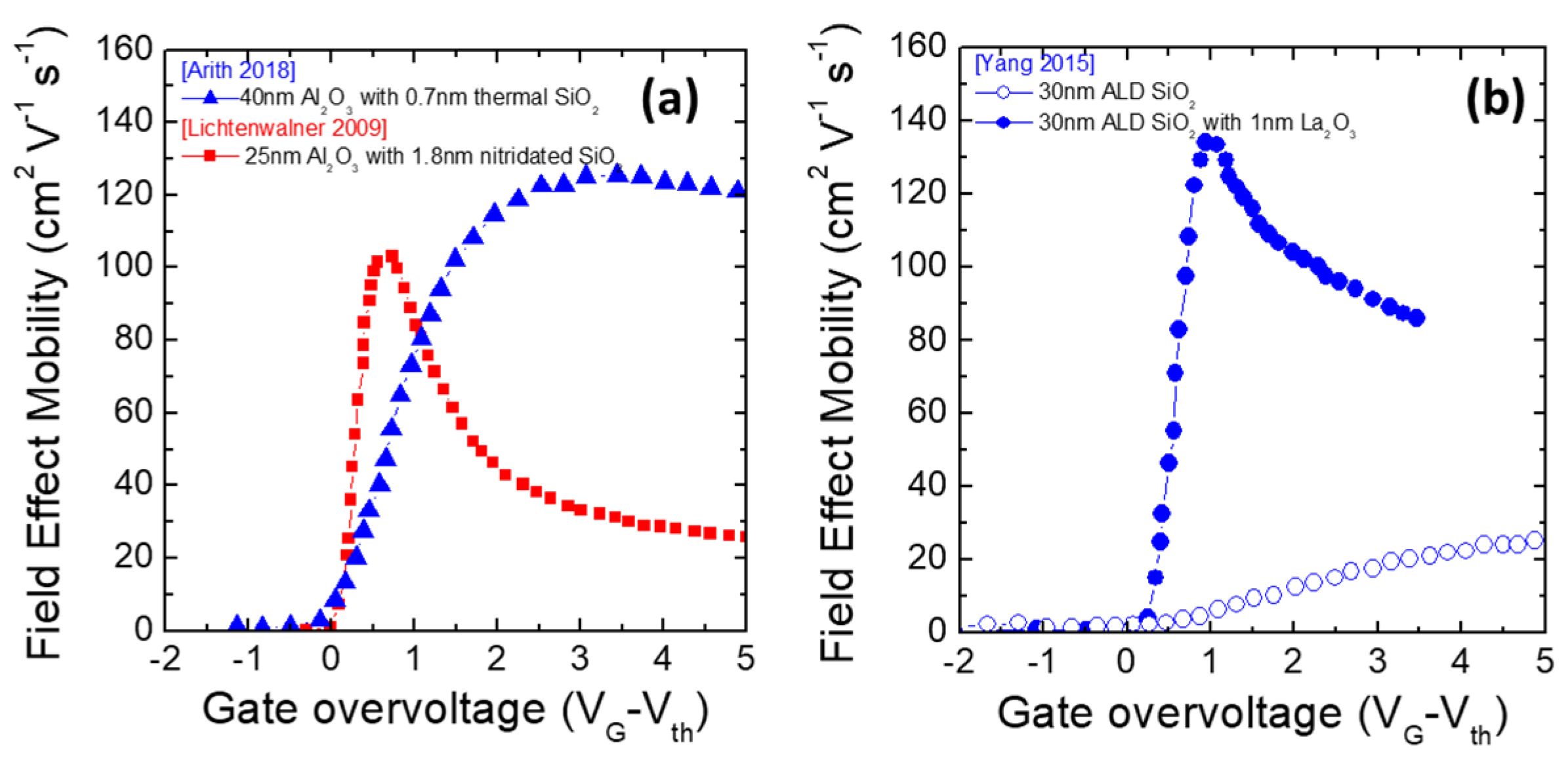
- Arith, F.; Urresti, J.; Vasilevskiy, K.; Olsen, S.; Wright, N.; O’Neill, A. Increased Mobility in Enhancement Mode 4H-SiC MOSFET Using a Thin SiO2/Al2O3 Gate Stack. IEEE Electron Device Lett. 2018, 39, 564–567. [Google Scholar] [CrossRef]
- Yang, X.; Lee, B.; Misra, V. Electrical Characteristics of SiO2 Deposited by Atomic Layer Deposition on 4H–SiC After Nitrous Oxide Anneal. IEEE Trans. Electron Devices 2016, 63, 2826–2830. [Google Scholar] [CrossRef]
- Yang, X.; Lee, B.; Misra, V. High Mobility 4H-SiC Lateral MOSFETs Using Lanthanum Silicate and Atomic Layer Deposited SiO2. IEEE Electron Device Lett. 2015, 36, 312–314. [Google Scholar] [CrossRef]
- Watanabe, H.; Kirino, T.; Uenishi, Y.; Chanthaphan, A.; Yoshigoe, A.; Teraoka, Y.; Mitani, S.; Nakano, Y.; Nakamura, T.; Hosoi, T.; et al. Impact of Stacked AlON/SiO2 Gate Dielectrics for SiC Power Devices. ECS Trans. 2011, 35, 265–274. [Google Scholar] [CrossRef]
- Hosoi, T.; Kagei, Y.; Kirino, T.; Watanabe, Y.; Kozono, K.; Mitani, S.; Nakano, Y.; Nakamura, T.; Watanabe, H. Improved Characteristics of 4H-SiC MISFET with AlON/Nitrided SiO2 Stacked Gate Dielectrics. Mater. Sci. Forum 2010, 645–648, 991–994. [Google Scholar] [CrossRef]
- Chanthaphan, A.; Hosoi, T.; Nakano, Y.; Nakamura, T.; Shimura, T.; Watanabe, H. Improved bias-temperature instability characteristics in SiC metal-oxide-semiconductor devices with aluminum oxynitride dielectrics. Appl. Phys. Lett. 2014, 104, 122105. [Google Scholar] [CrossRef]
- Jayawardhena, I.U.; Ramamurthy, R.P.; Morisette, D.; Ahyi, A.C.; Thorpe, R.; Kuroda, M.A.; Feldman, L.C.; Dhar, S. Effect of surface treatments on ALD Al2O3/4H-SiC metal–oxide–semiconductor field-effect transistors. J. Appl. Phys. 2021, 129, 75702. [Google Scholar] [CrossRef]
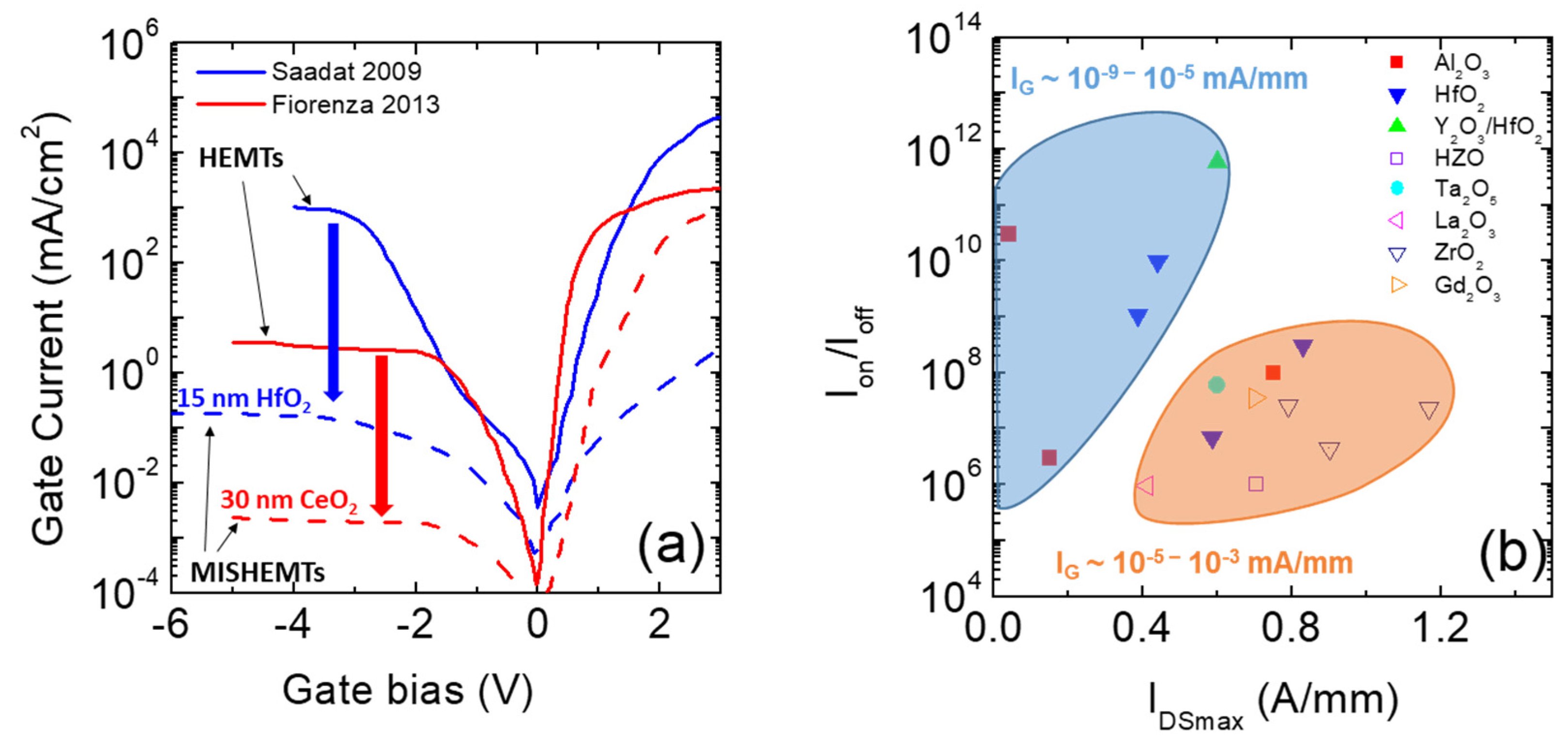
- Saadat, O.I.; Chung, J.W.; Piner, E.L.; Palacios, T. Gate-First AlGaN/GaN HEMT Technology for High-Frequency Applications. IEEE Electron Device Lett. 2009, 30, 1254–1256. [Google Scholar] [CrossRef]
- Zhang, Y.; Sun, M.; Joglekar, S.J.; Fujishima, T.; Palacios, T. Threshold voltage control by gate oxide thickness in fluorinated GaN metal-oxide-semiconductor high-electron-mobility transistors. Appl. Phys. Lett. 2013, 103, 33524. [Google Scholar] [CrossRef]
- Hou, B.; Ma, X.; Zhu, J.; Yang, L.; Chen, W.; Mi, M.; Zhu, Q.; Chen, L.; Zhang, R.; Zhang, M.; et al. 0.9-A/mm, 2.6-V Flash-Like Normally-Off Al2O3/AlGaN/GaN MIS-HEMTs Using Charge Trapping Technique. IEEE Electron Device Lett. 2018, 39, 397–400. [Google Scholar] [CrossRef]
- Schilirò, E.; Fiorenza, P.; Bongiorno, C.; Spinella, C.; Di Franco, S.; Greco, G.; Nigro, R.L.; Roccaforte, F. Correlating electron trapping and structural defects in Al2O3 thin films deposited by plasma enhanced atomic layer deposition. AIP Adv. 2020, 10, 125017. [Google Scholar] [CrossRef]
- Kubo, T.; Egawa, T. Electrical characteristics and interface properties of ALD-HfO2/AlGaN/GaN MIS-HEMTs fabricated with post-deposition annealing. Semicond. Sci. Technol. 2017, 32, 125016. [Google Scholar] [CrossRef]
- Huang, Z.; Liu, J.; Huang, X.; Yao, J.; Zhang, J.; Guo, Y. Analysis of Interface Properties in AlGaN/GaN MIS-HEMTs with HfO2 and SiNx Gate Dielectric. In Proceedings of the 2020 10th International Conference on Power and Energy Systems (ICPES), Chengdu, China, 25–27 December 2020; pp. 549–552. [Google Scholar]
- Liu, C.; Chor, E.F.; Tan, L.S. Investigations of HfO2/AlGaN/GaN metal-oxide-semiconductor high electron mobility transistors. Appl. Phys. Lett. 2006, 88, 173504. [Google Scholar] [CrossRef]
- Lin, Y.C.; Lin, T.W.; Wu, C.H.; Yao, J.N.; Hsu, H.T.; Shih, W.C.; Kakushima, K.; Tsutsui, K.; Iwai, H.; Chang, E.Y. Optimization of gate insulator material for GaN MIS-HEMT. In Proceedings of the 2016 28th International Symposium on Power Semiconductor Devices and ICs (ISPSD), Prague, Czech Republic, 12–16 June 2016; pp. 115–118. [Google Scholar] [CrossRef]
- Shi, Y.-T.; Xu, W.-Z.; Zeng, C.-K.; Ren, F.-F.; Ye, J.-D.; Zhou, D.; Chen, D.-J.; Zhang, R.; Zheng, Y.; Lu, H. High-k HfO2-Based AlGaN/GaN MIS-HEMTs With Y2O3 Interfacial Layer for High Gate Controllability and Interface Quality. IEEE J. Electron Devices Soc. 2020, 8, 15–19. [Google Scholar] [CrossRef]
- Cui, X.; Cheng, W.; Hua, Q.; Liang, R.; Hu, W.; Wang, Z.L. Enhanced performances of AlGaN/GaN HEMTs with dielectric engineering of HfZrOx. Nano Energy 2020, 68, 104361. [Google Scholar] [CrossRef]
- Kumar, S.; Kumar, H.; Vura, S.; Pratiyush, A.S.; Charan, V.S.; Dolmanan, S.B.; Tripathy, S.; Muralidharan, R.; Nath, D.N. Investigation of Ta2O5 as an Alternative High-k Dielectric for InAlN/GaN MOS-HEMT on Si. IEEE Trans. Electron Devices 2019, 66, 1230–1235. [Google Scholar] [CrossRef]
- Balachander, K.; Arulkumaran, S.; Ishikawa, H.; Baskar, K.; Egawa, T. Studies on electron beam evaporated ZrO2/AlGaN/GaN metal-oxide-semiconductor high-electron-mobility transistors. Phys. Status Solidi 2005, 202, R16–R18. [Google Scholar] [CrossRef]
- Kuzmik, J.; Pozzovivo, G.; Abermann, S.; Gonschorek, M.; Feltin, E.; Grandjean, N.; Bertagnolli, E.; Pogany, D.; Carlin, J.-F.; Strasser, G. Technology and Performance of InAlN/AlN/GaN HEMTs With Gate Insulation and Current Collapse Suppression Using ZrO2 or HfO2. IEEE Trans. Electron Devices 2008, 55, 937–941. [Google Scholar] [CrossRef]
- Ye, G.; Wang, H.; Arulkumaran, S.; Ng, G.I.; Hofstetter, R.; Li, Y.; Anand, M.J.; Ang, K.S.; Maung, Y.K.T.; Foo, S.C. Atomic layer deposition of ZrO2 as gate dielectrics for AlGaN/GaN metal-insulator-semiconductor high electron mobility transistors on silicon. Appl. Phys. Lett. 2013, 103, 142109. [Google Scholar] [CrossRef]
- Gao, Z.; Romero, M.F.; Redondo-Cubero, A.; Pampillon, M.A.; Andres, E.S.; Calle, F. Effects of Gd2O3 Gate Dielectric on Proton-Irradiated AlGaN/GaN HEMTs. IEEE Electron Device Lett. 2017, 38, 611–614. [Google Scholar] [CrossRef]
- Fiorenza, P.; Schilirò, E.; Greco, G.; Vivona, M.; Cannas, M.; Giannazzo, F.; Nigro, R.L.; Roccaforte, F. Temperature and time dependent electron trapping in Al2O3 thin films onto AlGaN/GaN heterostructures. Appl. Surf. Sci. 2021, 579, 152136. [Google Scholar] [CrossRef]
- Li, Z.; Chow, T.P. Channel scaling of hybrid GaN MOS-HEMTs. Solid-State Electron. 2011, 56, 111–115. [Google Scholar] [CrossRef]
- Roccaforte, F.; Greco, G.; Fiorenza, P.; Iucolano, F. An Overview of Normally-Off GaN-Based High Electron Mobility Transistors. Materials 2019, 12, 1599. [Google Scholar] [CrossRef] [PubMed]
- Fiorenza, P.; Greco, G.; Iucolano, F.; Patti, A.; Roccaforte, F. Slow and fast traps in metal-oxide-semiconductor capacitors fabricated on recessed AlGaN/GaN heterostructures. Appl. Phys. Lett. 2015, 106, 142903. [Google Scholar] [CrossRef]
- Hosoi, T.; Watanabe, K.; Nozaki, M.; Yamada, T.; Shimura, T.; Watanabe, H. Mobility enhancement in recessed-gate AlGaN/GaN MOS-HFETs using an AlON gate insulator. Jpn. J. Appl. Phys. 2019, 58, SCCD16. [Google Scholar] [CrossRef]
- Oka, T.; Nozawa, T. AlGaN/GaN Recessed MIS-Gate HFET With High-Threshold-Voltage Normally-Off Operation for Power Electronics Applications. IEEE Electron Device Lett. 2008, 29, 668–670. [Google Scholar] [CrossRef]
- Greco, G.; Fiorenza, P.; Iucolano, F.; Severino, A.; Giannazzo, F.; Roccaforte, F. Conduction Mechanisms at Interface of AlN/SiN Dielectric Stacks with AlGaN/GaN Heterostructures for Normally-off High Electron Mobility Transistors: Correlating Device Behavior with Nanoscale Interfaces Properties. ACS Appl. Mater. Interfaces 2017, 9, 35383–35390. [Google Scholar] [CrossRef]
- Asahara, R.; Nozaki, M.; Yamada, T.; Ito, J.; Nakazawa, S.; Ishida, M.; Ueda, T.; Yoshigoe, A.; Hosoi, T.; Shimura, T.; et al. Effect of nitrogen incorporation into Al-based gate insulators in AlON/AlGaN/GaN metal–oxide–semiconductor structures. Appl. Phys. Express 2016, 9, 101002. [Google Scholar] [CrossRef]
- Im, K.-S.; Ha, J.-B.; Kim, K.-W.; Lee, J.-S.; Kim, D.-S.; Hahm, S.-H.; Lee, J.-H. Normally off GaN MOSFET Based on AlGaN/GaN Heterostructure with Extremely High 2DEG Density Grown on Silicon Substrate. IEEE Electron Device Lett. 2010, 31, 192–194. [Google Scholar] [CrossRef]
- Kim, K.-W.; Jung, S.-D.; Kim, D.-S.; Kang, H.-S.; Im, K.-S.; Oh, J.-J.; Ha, J.-B.; Shin, J.-K.; Lee, J.-H. Effects of TMAH Treatment on Device Performance of Normally off Al2O3/GaN MOSFET. IEEE Electron Device Lett. 2011, 32, 1376–1378. [Google Scholar] [CrossRef]
- Wang, Y.; Wang, M.; Xie, B.; Wen, C.P.; Wang, J.; Hao, Y.; Wu, W.; Chen, K.J.; Shen, B. High-Performance Normally-Off Al2O3/GaN MOSFET Using a Wet Etching-Based Gate Recess Technique. IEEE Electron Device Lett. 2013, 34, 1370–1372. [Google Scholar] [CrossRef]
- Wang, M.; Wang, Y.; Zhang, C.; Xie, B.; Wen, C.P.; Wang, J.; Hao, Y.; Wu, W.; Chen, K.J.; Shen, B. 900 V/1.6 mΩ⋅cm2 Normally Off Al2O3/GaN MOSFET on Silicon Substrate. IEEE Trans. Electron Devices 2014, 61, 2035–2040. [Google Scholar] [CrossRef]
- Yao, Y.; He, Z.; Yang, F.; Shen, Z.; Zhang, J.; Ni, Y.; Li, J.; Wang, S.; Zhou, G.; Zhong, J.; et al. Normally-off GaN recessed-gate MOSFET fabricated by selective area growth technique. Appl. Phys. Express 2013, 7, 16502. [Google Scholar] [CrossRef]
- He, L.; Yang, F.; Li, L.; Chen, Z.; Shen, Z.; Zheng, Y.; Yao, Y.; Ni, Y.; Zhou, D.; Zhang, X.; et al. High Threshold Voltage Uniformity and Low Hysteresis Recessed-Gate Al2O3/AlN/GaN MISFET by Selective Area Growth. IEEE Trans. Electron Devices 2017, 64, 1554–1560. [Google Scholar] [CrossRef]
- Tao, M.; Liu, S.; Xie, B.; Wen, C.P.; Wang, J.; Hao, Y.; Wu, W.; Cheng, K.; Shen, B.; Wang, M. Characterization of 880 V Normally Off GaN MOSHEMT on Silicon Substrate Fabricated With a Plasma-Free, Self-Terminated Gate Recess Process. IEEE Trans. Electron Devices 2018, 65, 1453–1457. [Google Scholar] [CrossRef]
- Ťapajna, M.; Válik, L.; Gucmann, F.; Gregusova, D.; Fröhlich, K.; Haščík, Š.; Dobročka, E.; Tóth, L.; Pécz, B.; Kuzmík, J. Low-temperature atomic layer deposition-grown Al2O3 gate dielectric for GaN/AlGaN/GaN MOS HEMTs: Impact of deposition conditions on interface state density. J. Vac. Sci. Technol. B 2017, 35, 1A107. [Google Scholar] [CrossRef]
- Fiorenza, P.; Greco, G.; Schilirò, E.; Iucolano, F.; Nigro, R.L.; Roccaforte, F. Determining oxide trapped charges in Al2O3 insulating films on recessed AlGaN/GaN heterostructures by gate capacitance transients measurements. Jpn. J. Appl. Phys. 2018, 57, 050307. [Google Scholar] [CrossRef]
- Zhao, Y.; Wang, C.; Zheng, X.; Ma, X.; He, Y.; Liu, K.; Li, A.; Peng, Y.; Zhang, C.; Hao, Y. Effects of recess depths on performance of AlGaN/GaN power MIS-HEMTs on the Si substrates and threshold voltage model of different recess depths for the using HfO2 gate insulator. Solid-State Electron. 2020, 163, 107649. [Google Scholar] [CrossRef]
- Anderson, T.J.; Wheeler, V.D.; Shahin, D.I.; Tadjer, M.J.; Koehler, A.D.; Hobart, K.D.; Christou, A.; Kub, F.J.; Eddy, C.R. Enhancement mode AlGaN/GaN MOS high-electron-mobility transistors with ZrO2 gate dielectric deposited by atomic layer deposition. Appl. Phys. Express 2016, 9, 11–14. [Google Scholar] [CrossRef]
- Jiang, H.; Tang, C.W.; Lau, K.M. Enhancement-Mode GaN MOS-HEMTs With Recess-Free Barrier Engineering and High- k ZrO2 Gate Dielectric. IEEE Electron Device Lett. 2018, 39, 405–408. [Google Scholar] [CrossRef]
- Cai, Y.; Zhang, Y.; Liang, Y.; Mitrovic, I.Z.; Wen, H.; Liu, W.; Zhao, C. Low on -State Resistance Normally- off AlGaN/GaN MIS-HEMTs with Partially Recessed Gate and ZrOx. IEEE Trans. Electron Devices 2021, 68, 4310–4316. [Google Scholar] [CrossRef]
- Hu, Q.; Li, S.; Li, T.; Wang, X.; Li, X.; Wu, Y. Channel Engineering of Normally-OFF AlGaN/GaN MOS-HEMTs by Atomic Layer Etching and High-κ Dielectric. IEEE Electron Device Lett. 2018, 39, 1377–1380. [Google Scholar] [CrossRef]
- Lin, Y.C.; Huang, Y.X.; Huang, G.N.; Wu, C.H.; Yao, J.N.; Chu, C.M.; Chang, S.; Hsu, C.C.; Lee, J.H.; Kakushima, K.; et al. Enhancement-Mode GaN MIS-HEMTs With LaHfOx Gate Insulator for Power Application. IEEE Electron Device Lett. 2017, 38, 1101–1104. [Google Scholar] [CrossRef]
- Greco, G.; Iucolano, F.; Roccaforte, F. Review of technology for normally-off HEMTs with p-GaN gate. Mater. Sci. Semicond. Process. 2018, 78, 96–106. [Google Scholar] [CrossRef]
- Li, Y.; Guo, Y.; Zhang, K.; Zou, X.; Wang, J.; Kong, Y.; Chen, T.; Jiang, C.; Fang, G.; Liu, C.; et al. Positive Shift in Threshold Voltage Induced by CuO and NiOx Gate in AlGaN/GaN HEMTs. IEEE Trans. Electron Devices 2017, 64, 3139–3144. [Google Scholar] [CrossRef]
- Kaneko, N.; Machida, O.; Yanagihara, M.; Iwakami, S.; Baba, R.; Goto, H.; Iwabuchi, A. Normally-off AlGaN/GaN HFETs using NiOx gate with recess. In Proceedings of the 2009 21st International Symposium on Power Semiconductor Devices & IC’s, Barcelona, Spain, 14–18 June 2009; pp. 25–28. [Google Scholar] [CrossRef]
- Wang, L.; Li, L.; Xie, T.; Wang, X.; Liu, X.; Ao, J.-P. Threshold voltage tuning in AlGaN/GaN HFETs with p-type Cu2O gate synthesized by magnetron reactive sputtering. Appl. Surf. Sci. 2018, 437, 98–102. [Google Scholar] [CrossRef]
- Kohmoto, O.; Nakagawa, H.; Isagawa, Y.; Chayahara, A. Effect of heat treatment on the oxygen content and resistivity in sputtered NiO films. J. Magn. Magn. Mater. 2001, 226–230, 1629–1630. [Google Scholar] [CrossRef]
- Raebiger, H.; Lany, S.; Zunger, A. Origins of thep-type nature and cation deficiency in Cu2O and related materials. Phys. Rev. B 2007, 76, 45209. [Google Scholar] [CrossRef]


| Oxide | Dielectric Constant | Band Gap (eV) | Crystallization Temperature | Ref |
|---|---|---|---|---|
| Al2O3 | 10 | 9 | 900 °C | [17,18] |
| HfO2 | ~20 | 5.6–5.8 | 500 °C | [17,18,22] |
| NiO | 11.7 | 4 | 300 °C | [23,24] |
| CeO2 | 26 | 6 | 500 °C | [25] |
| Sc2O3 | 12–14 | 6.0 | >400 °C | [26,27,28,29] |
| Y2O3 | 10 | 5.5 | >400 °C | [26,28,29] |
| Gd2O3 | ~20 | 5.0–5.45 | >400 °C | [26,28] |
| La2O3 | ~20 | 5.4–5.6 | >400 °C | [17,18,27,29] |
| ZrO2 | 25 | 5.8 | >400 °C | [17,18] |
| Ga2O3 | ~10 | 5 | >500 °C | [30] |
| ALD | MBE | CVD | PVD | |
|---|---|---|---|---|
| Thickness range | ≤2000 Å | ≤2000 Å | ≥100 Å | ≥100 Å |
| Deposition rate | Low 1–5 nm/min | High 0.01–0.3 µm/min | High 1–10 µm/h | Medium 0.1–1 µm/h |
| Step coverage Aspect ratio | 100% 60:1 | 25–50% 1:1 | 70% 1:1 | 25–50% 1:1 |
| Deposition temperature | 25–400 °C | 500–1000 °C | 300–1100 °C | 200–500 °C |
| Film type availability | High (limited for metals) | High (limited for Metals) | High (limited for metals) | High for metals and conductive materials |
| Oxide | Dielectric Constant | Lattice Constant (Å) | Mismatch to (0001) GaN (%) | Deposition Technique | Ref. |
|---|---|---|---|---|---|
| Gd2O3 | 9 | 10.813 | 20.1 | MBE | [82] |
| Sc2O3 | 13–14 | 9.845 | 9.2 | PVD and MBE | [83,84] |
| La2O3 | 18–27 | 4.211 | 6.5 | MBE | [83] |
| CeO2 | 15–26 | 5.411 | 6 | MOCVD | [25,81] |
| NiO | 11.9 | 4.177 | 5 | Thermal oxidation or MOCVD | [23,24,81] |
| Gate Insulator | Thickness (nm) | Vth (V) | µFE (cm2V−1s−1) | Dit (cm−2eV) at EC − Et = 0.2 eV | Ref. |
|---|---|---|---|---|---|
| Al2O3 | 35 | 2.8 | 64 | 8 × 10¹¹ | [108] |
| Al2O3 | 33 | 0.5 -3 | 52 | 1 × 1011 cm−2 (integral) | [117] |
| Al2O3 on SiO2 | 35 + 2 | 2.8 | 18 | 8 × 10¹¹ | [108] |
| 35 + 0.7 | 2.8 | 300 | 5 × 10¹¹ | [108] | |
| 40 + 0.7 | 2 | 120 | 6 × 10¹¹ | [111] | |
| 25 + 1.8 | 0.8 | 106 | - | [43] | |
| SiO2 on La2O3 | 30 + 1 | 3 | 132 | - | [113] |
| AlON | 60 + 10 | > 0 | 26.9 | 1 × 10¹¹ | [115] |
| Dielectric | Thickness (nm) | Vth (V) | IDmax (mA/mm) | IG-leak (mA/mm) | ION/IOFF | Ref. |
|---|---|---|---|---|---|---|
| Al2O3 | 25 | −7.0 | 150 | 5.0 × 10⁻⁵ | 3.0 × 10⁶ | [119] |
| 15 | −7.0 | 750 | 8.0 × 10⁻⁵ | 1.0 × 10⁸ | [120] | |
| 30 | −8.0 | 40 | 1.0 × 10⁻⁸ | 3.0 × 10¹⁰ | [121] | |
| HfO2 | 20 | −1.1 | 440 | 2.2 × 10⁻⁷ | 1.0 × 10¹⁰ | [122] |
| 12 | −8.0 | 386 | 1.1 × 10⁻⁹ | 1.1 × 10⁹ | [123] | |
| 23 | −6.0 | 830 | 3.0 × 10⁻⁶ | 3.0 × 10⁸ | [124] | |
| 8 | −3.7 | 585 | 6.5 × 10⁻⁵ | 6.9 × 10⁶ | [125] | |
| Y2O3/HfO2 | 1/12 | −5.0 | 600 | 3.0 × 10⁻⁹ | 6.0 × 10¹¹ | [126] |
| Ta2O5 | 24 | −9.7 | 600 | 1.0 × 10⁻⁵ | 6.0 × 10⁷ | [128] |
| La2O3 | 8 | −2.9 | 409 | 1.0 × 10⁻⁴ | 9.7 × 10⁵ | [125] |
| ZrO2 | 30 | −7 | 1168 | 5.4 × 10⁻⁴ | 2.3 × 10⁷ | [129] |
| 10 | −4.2 | 900 | 2.0 × 10⁻⁴ | 4.5 × 10⁶ | [130] | |
| 10 | −3.9 | 790 | 3.0 × 10⁻⁵ | 2.6 × 10⁷ | [131] | |
| HfZrOx | 20 | −12 | 705 | 6.0 × 10⁻⁴ | 1.0 × 10⁷ | [127] |
| Gd2O3 | 4 | −6.5 | 700 | 1.0 × 10⁻⁶ | 3.5 × 10⁷ | [132] |
Publisher’s Note: MDPI stays neutral with regard to jurisdictional claims in published maps and institutional affiliations. |
© 2022 by the authors. Licensee MDPI, Basel, Switzerland. This article is an open access article distributed under the terms and conditions of the Creative Commons Attribution (CC BY) license (https://creativecommons.org/licenses/by/4.0/).
Share and Cite
Lo Nigro, R.; Fiorenza, P.; Greco, G.; Schilirò, E.; Roccaforte, F. Structural and Insulating Behaviour of High-Permittivity Binary Oxide Thin Films for Silicon Carbide and Gallium Nitride Electronic Devices. Materials 2022, 15, 830. https://doi.org/10.3390/ma15030830
Lo Nigro R, Fiorenza P, Greco G, Schilirò E, Roccaforte F. Structural and Insulating Behaviour of High-Permittivity Binary Oxide Thin Films for Silicon Carbide and Gallium Nitride Electronic Devices. Materials. 2022; 15(3):830. https://doi.org/10.3390/ma15030830
Chicago/Turabian StyleLo Nigro, Raffaella, Patrick Fiorenza, Giuseppe Greco, Emanuela Schilirò, and Fabrizio Roccaforte. 2022. "Structural and Insulating Behaviour of High-Permittivity Binary Oxide Thin Films for Silicon Carbide and Gallium Nitride Electronic Devices" Materials 15, no. 3: 830. https://doi.org/10.3390/ma15030830
APA StyleLo Nigro, R., Fiorenza, P., Greco, G., Schilirò, E., & Roccaforte, F. (2022). Structural and Insulating Behaviour of High-Permittivity Binary Oxide Thin Films for Silicon Carbide and Gallium Nitride Electronic Devices. Materials, 15(3), 830. https://doi.org/10.3390/ma15030830