
Influence of a Two-Dimensional Growth Mode on Electrical Properties of the GaN Buffer in an AlGaN/GaN High Electron Mobility Transistor


Abstract
:1. Introduction
2. Experimental Section
3. Results and Discussion
4. Conclusions
Author Contributions
Funding
Institutional Review Board Statement
Informed Consent Statement
Data Availability Statement
Conflicts of Interest
References
- Mandal, S.; Kanathila, M.B.; Pynn, C.D.; Li, W.; Gao, J.; Margalith, T.; Laurent, M.A.; Chowdhury, S. Observation and discussion of avalanche electroluminescence in GaN p-n diodes offering a breakdown electric field of 3 MV cm−1. Semicond. Sci. Technol. 2018, 33, 065013. [Google Scholar] [CrossRef]
- Huang, A. New Unipolar Switching Power Device Figures of Merit. IEEE Electron. Device Lett. 2004, 25, 298–301. [Google Scholar] [CrossRef]
- Hudgins, J.; Simin, G.; Santi, E.; Khan, M. An assessment of wide bandgap semiconductors for power devices. IEEE Trans. Power Electron. 2003, 18, 907–914. [Google Scholar] [CrossRef]
- Dimitriev, V.A.; Irvine, K.G.; Carter, C.H.; Kuznetsov, N.I.; Kalinina, E.V. Electric breakdown in GaN p-n junctions. Appl. Phys. Lett. 1996, 68, 229–231. [Google Scholar]
- Meneghesso, G.; Meneghini, M.; Zanoni, E. Breakdown mechanisms in AlGaN/GaN HEMTs: An overview. Jpn. J. Appl. Phys. 2014, 53, 100211. [Google Scholar] [CrossRef]
- Hashimoto, S.; Akita, K.; Tanabe, T.; Nakahata, H.; Takeda, K.; Amano, H. Epitaxial layers of AlGaN channel HEMTs on AlN substrates. SEI Tech. Rev. 2010, 71, 83–87. [Google Scholar]
- Chow, T.; Tyagi, R. Wide bandgap compound semiconductors for superior high-voltage unipolar power devices. IEEE Trans. Electron. Devices 1994, 41, 1481–1483. [Google Scholar] [CrossRef]
- Kaplar, R.J.; Allerman, A.A.; Armstrong, A.M.; Baca, A.G.; Fischer, A.J.; Wierer, J.J.; Neely, J.C. (Invited) Ultra-Wide-Bandgap Semiconductors for Power Electronics. ECS Meet. Abstr. 2015, MA2015-02, 1119. [Google Scholar] [CrossRef]
- Sun, Y.; Kang, X.; Zheng, Y.; Lu, J.; Tian, X.; Wei, K.; Wu, H.; Wang, W.; Liu, X.; Zhang, G. Review of the recent progress on GaN-Based vertical power Schottky Barrier Diodes (SBDs). Electronics 2019, 8, 575. [Google Scholar]
- Harima, H. Properties of GaN and related compounds studied by means of Raman scattering. J. Phys. Condens. Matter 2002, 14, R967–R993. [Google Scholar] [CrossRef]
- Sumiyoshi, K.; Okada, M.; Ueno, M.; Kiyama, M.; Nakamura, T. Low on-resistance high breakdown Voltage GaN diodes on low dislocation density GaN substrates. SEI Tech. Rev. 2013, 77, 113–117. [Google Scholar]
- Ozbek, A.M.; Baliga, B.J. Planar Nearly Ideal Edge-Termination Technique for GaN Devices. IEEE Electron. Device Lett. 2011, 32, 300–302. [Google Scholar] [CrossRef]
- Kong, Y.; Zheng, Y.; Zhou, C.; Gu, S.; Zhang, R.; Han, P.; Shi, Y.; Jiang, R. Two-dimensional electron gas densities in AlGaN/AlN/GaN heterostructures. Appl. Phys. A 2006, 84, 95–98. [Google Scholar] [CrossRef]
- Mimura, T. The early history of the high electron mobility transistor (HEMT). IEEE Trans. Microw. Theory Tech. 2002, 50, 780–782. [Google Scholar] [CrossRef]
- Smith, P.; Chao, P.; Dub, K.; Lester, L.; Lee, B.; Ballingall, J. Advances in HEMT Technology and Applications. IEEE MTT-S Digest 1987, S-2, 749–752. [Google Scholar] [CrossRef]
- Medjdoub, F.; Herbecq, N.; Linge, A.; Zegaoui, M. High frequency high breakdown voltage GaN transistors. In Proceedings of theIEEE International Electron Devices Meeting (IEDM) 2015, Washington, DC, USA, 7–9 December 2015; pp. 217–220. [Google Scholar]
- Chung, J.W.; Hoke, W.E.; Chumbes, E.M.; Palacios, T. AlGaN/GaN HEMT With 300-GHz fmax. IEEE Electron. Device Lett. 2010, 31, 195–197. [Google Scholar] [CrossRef]
- Rodriguez, M.; Zhang, Y.; Maksimović, D. High-frequency PWM buck converters using GaN-on-SiC HEMTs. IEEE Trans. Power Electron. 2014, 29, 2462–2473. [Google Scholar] [CrossRef]
- Wu, Y.F.; Kapolnek, D.; Ibbetson, J.P.; Parikh, P.; Keller, B.P.; Mishra, U.K. Very-high power density AlGaN/GaN HEMTs. IEEE Trans. Electron. Devices 2001, 48, 586–590. [Google Scholar]
- Lin, Y.C.; Chen, S.H.; Lee, P.H.; Lai, K.H.; Huang, T.J.; Chang, E.Y.; Hsu, H.-T. Gallium Nitride (GaN) High-Electron-Mobility Transistors with Thick Copper Metallization Featuring a Power Density of 8.2 W/mm for Ka-Band Applications. Micromachines 2020, 11, 222. [Google Scholar] [CrossRef]
- Li, X.; Hove, M.V.; Zhao, M.; Geens, K.; Lempinen, V.-P.; Sormunen, J.; Groeseneken, G.; Decoutere, S. 200 V Enhancement-mode p-GaN HEMTs fabricated on 200 mm GaN-on-SOI with trench isolation for monolithic integration. IEEE Electron. Device Lett. 2017, 38, 918–921. [Google Scholar] [CrossRef]
- Wong, M.; Chowdhury, U.; Sicault, D.; Becher, D.; Denyszyn, J.; Zhu, T.; Feng, M.; Dupuis, R. Delta-doped AlGaN/AlN/GaN microwave HFETs grown by metalorganic chemical vapour deposition. Electron. Lett. 2002, 38, 428–429. [Google Scholar] [CrossRef]
- Wang, J.; You, H.; Guo, H.; Xue, J.; Yang, G.; Chen, D.; Liu, B.; Lu, H.; Zhang, R.; Zheng, Y. Do all screw dislocations cause leakage in GaN-based devices? Appl. Phys. Lett. 2020, 116, 062104. [Google Scholar] [CrossRef]
- Zhou, C.; Jiang, Q.; Huang, S.; Chen, K.J. Vertical leakage/breakdown mechanisms in AlGaN/GaN-on-Si devices. IEEE Electron Device Lett. 2012, 33, 1132–1134. [Google Scholar] [CrossRef]
- Usami, S.; Ando, Y.; Tanaka, A.; Nagamatsu, K.; Deki, M.; Kushimoto, M.; Nitta, S.; Honda, Y.; Amano, H.; Sugawara, Y.; et al. Correlation between dislocations and leakage current of p-n diodes on a free-standing GaN substrate. Appl. Phys. Lett. 2018, 112, 182106. [Google Scholar] [CrossRef]
- Hsu, J.W.P.; Manfra, M.J.; Molnar, R.J.; Heying, B.; Speck, J.S. Direct imaging of reverse-bias leakage through pure screw dislocations in GaN films grown by molecular beam epitaxy on GaN templates. Appl. Phys. Lett. 2002, 81, 79–81. [Google Scholar] [CrossRef] [Green Version]
- Rowena, I.B.; Selvaraj, S.L.; Egawa, T. Buffer Thickness Contribution to Suppress Vertical Leakage Current with High Breakdown Field (2.3 MV/cm) for GaN on Si. IEEE Electron. Device Lett. 2011, 32, 1534–1536. [Google Scholar] [CrossRef]
- Tang, H.; Webb, J.B.; Bardwell, J.; Raymond, S.; Salzman, J.; Uzan-Saguy, C. Properties of carbon-doped GaN. Appl. Phys. Lett. 2001, 78, 757–759. [Google Scholar] [CrossRef]
- Chen, J.T.; Forsberg, U.; Janzen, E. Impact of residual carbon on two-dimensional electron Gas properties in AlxGa1-xN/GaN heterostructure. Appl. Phys. Lett. 2013, 102, 193506. [Google Scholar] [CrossRef]
- Wang, T.; Bai, J.; Parbrook, P.J.; Cullis, A.G. Air-bridged lateral growth of an Al0.98Ga0.02N layer by introduction of porosity in an AlN buffer. Appl. Phys. Lett. 2005, 87, 151906. [Google Scholar] [CrossRef]
- Bai, J.; Wang, T.; Parbrook, P.; Lee, K.; Cullis, A. A study of dislocations in AlN and GaN films grown on sapphire substrates. J. Cryst. Growth 2005, 282, 290–296. [Google Scholar] [CrossRef]
- Wang, Q.; Wang, T.; Bai, J.; Cullis, A.G.; Parbrook, P.J.; Ranalli, F. Growth and optical investigation of self-assembled InGaN quantum dots on a GaN surface using a high temperature AlN buffer. J. Appl. Phys. 2008, 103, 123522. [Google Scholar] [CrossRef]
- Wang, Q.; Gong, Y.P.; Zhang, J.; Bai, J.; Ranalli, F.; Wang, T. Stimulated emission at 340 nm from AlGaN multiple quantum well grown using high temperature AlN buffer technologies on sapphire. Appl. Phys. Lett. 2009, 95, 161904. [Google Scholar] [CrossRef]
- Davies, S.C.; Mowbray, D.J.; Wang, Q.; Ranalli, F.; Wang, T. Influence of crystal quality of underlying GaN buffer on the formation and optical properties of InGaN/GaN quantum dots. Appl. Phys. Lett. 2009, 95, 101909. [Google Scholar] [CrossRef]
- Jiang, S.; Cai, Y.; Feng, P.; Shen, S.; Zhao, X.; Fletcher, P.; Esendag, V.; Lee, K.-B.; Wang, T. Exploring an Approach toward the Intrinsic Limits of GaN Electronics. ACS Appl. Mater. Interfaces 2020, 12, 12949–12954. [Google Scholar] [CrossRef]
- Cristea, M. Capacitance-voltage profiling techniques for characterization of semiconductor materials and devices. Emerg. Trends Electr. Electron. Instrum. Eng. Int. J. 2014, 1, 29–38. [Google Scholar] [CrossRef] [Green Version]
- Jian-Zhi, Z.; Zhao-Jun, L.; Corrigan, T.D.; Yu, Z.; Yuan-Jie, L.; Wu, L.; Zhan-Guo, W.; Hong, C. Determination of the relative permittivity of the AlGaN barrier layer in strained AlGaN/GaN heterostructures. Chin. Phys. B 2009, 18, 3980–3984. [Google Scholar] [CrossRef]
- Ikeda, N.; Niiyama, Y.; Kambayashi, H.; Sato, Y.; Nomura, T.; Kato, S.; Yoshida, S. GaN Power Transistors on Si Substrates for Switching Applications. Proc. IEEE 2010, 98, 1151–1161. [Google Scholar] [CrossRef]


| Sample | Layer | Temperature [°C] | Pressure [Torr] | NH3 Flow Rate [sccm] | TMGa Flow Rate [sccm] | TMAl Flow Rate [sccm] |
|---|---|---|---|---|---|---|
| A | AlGaN Barrier | 1100 | 75 | 5480 | 12.5 | 30 |
| AlN Spacer | 1100 | 75 | 5480 | 30 | ||
| GaN Channel | 1100 | 75 | 5480 | 12.5 | ||
| 1.5 μm GaN Buffer | 1100 | 225 | 5480 | 65 | ||
| 25 nm LT GaN Nucleation Layer | 550 | 65 | 1900 | 65 | ||
| B | AlGaN Barrier | 1110 | 75 | 5480 | 12.5 | 30 |
| AlN Spacer | 1110 | 75 | 5480 | 30 | ||
| GaN Channel | 1100 | 75 | 5480 | 12.5 | ||
| 1.5 μm GaN Buffer | 1110 | 225 | 5480 | 65 | ||
| HT-AlN Buffer | 1180 | 65 | 5480 | 180 | ||
| C | AlGaN Barrier | 1108 | 75 | 5480 | 12.5 | 30 |
| AlN Spacer | 1108 | 75 | 5480 | 30 | ||
| GaN Channel | 1108 | 75 | 5480 | 12.5 | ||
| 1.5 μm GaN Buffer | 1108 | 175 | 5480 | 65 | ||
| HT-AlN Buffer | 1180 | 65 | 5480 | 180 | ||
| D | AlGaN Barrier | 1130 | 75 | 5480 | 12.5 | 30 |
| AlN Spacer | 1130 | 75 | 5480 | 30 | ||
| GaN Channel | 1130 | 75 | 5480 | 12.5 | ||
| 1.5 μm GaN Buffer | 1130 | 175 | 5480 | 65 | ||
| HT-AlN Buffer | 1180 | 65 | 5480 | 180 |
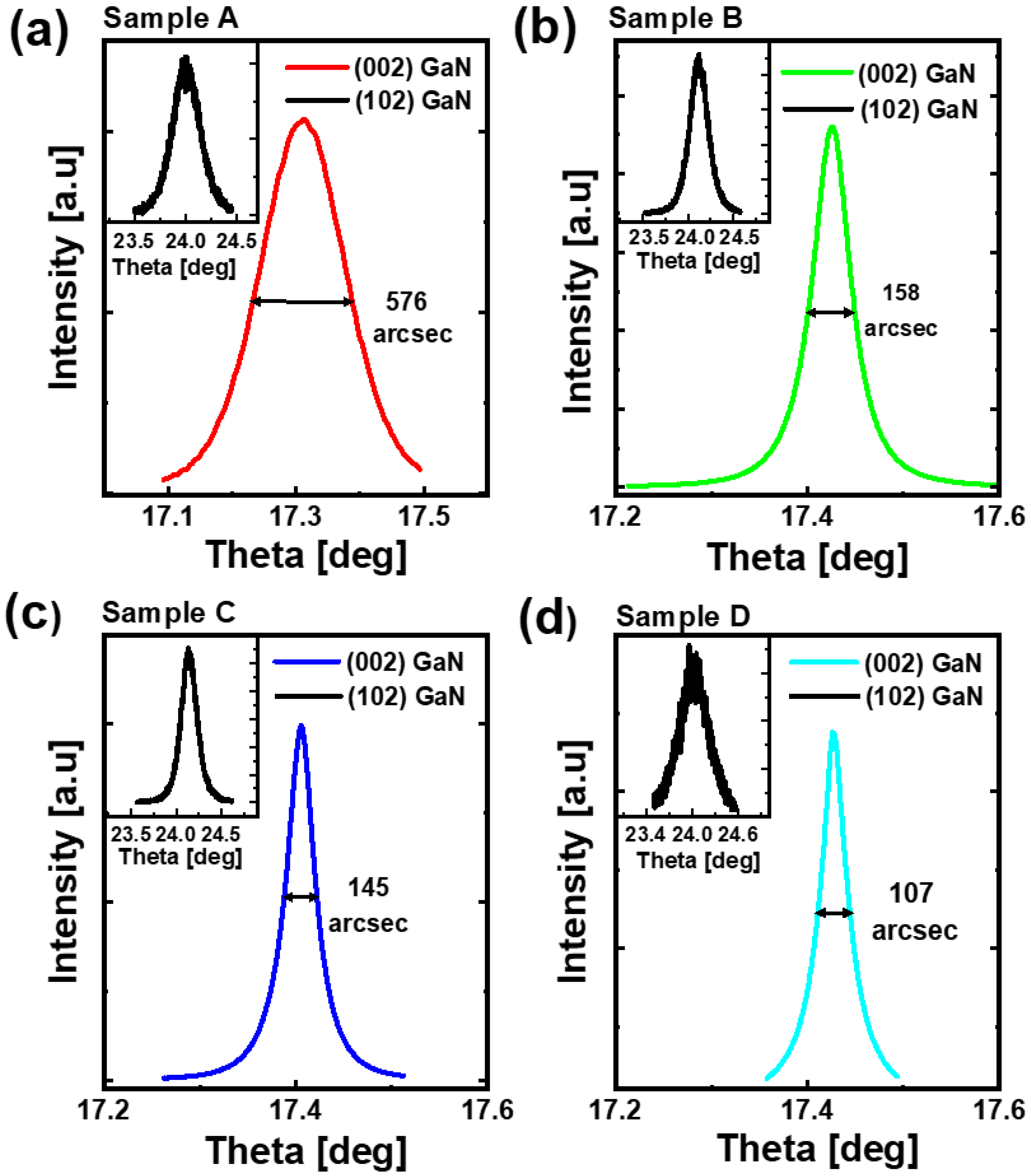
| Sample | (002) GaN FWHM [°] | Screw Dislocation Density [cm−2] | (102) GaN FWHM [°] | Mixed Dislocation Density [cm−2] |
|---|---|---|---|---|
| A | 0.1599 | 6.7 × 10⁸ | 0.3005 | 8.6 × 10⁹ |
| B | 0.0438 | 5.0 × 10⁷ | 0.2363 | 5.3 × 10⁹ |
| C | 0.0402 | 4.2 × 10⁷ | 0.1948 | 3.6 × 10⁹ |
| D | 0.0296 | 2.3 × 10⁷ | 0.4429 | 1.9 × 10¹⁰ |
| Sample | Dscrew [cm−2] | Calculated Nunintentional [cm−3] | Buffer Leakage, 2 µm@20 V [pA] | HEMT Current Density, Lg = 10 µm [mA/mm] | Breakdown Limit of Buffer [MV/cm] |
|---|---|---|---|---|---|
| A | 6.7 × 10⁸ | 1.0 × 10¹⁶ | 1136.4 | 1024 | 0.25 |
| B | 5.0 × 10⁷ | 1.0 × 10¹⁵ | 980.9 | 1086 | 0.6 |
| C | 4.2 × 10⁷ | 5.0 × 10¹⁴ | 615.0 | 920 | 1.9 |
| D | 2.3 × 10⁷ | 2.0 × 10¹⁴ | 41.7 | 582 | 2.5 |
Publisher’s Note: MDPI stays neutral with regard to jurisdictional claims in published maps and institutional affiliations. |
© 2022 by the authors. Licensee MDPI, Basel, Switzerland. This article is an open access article distributed under the terms and conditions of the Creative Commons Attribution (CC BY) license (https://creativecommons.org/licenses/by/4.0/).
Share and Cite
Esendag, V.; Feng, P.; Zhu, C.; Ni, R.; Bai, J.; Wang, T. Influence of a Two-Dimensional Growth Mode on Electrical Properties of the GaN Buffer in an AlGaN/GaN High Electron Mobility Transistor. Materials 2022, 15, 6043. https://doi.org/10.3390/ma15176043
Esendag V, Feng P, Zhu C, Ni R, Bai J, Wang T. Influence of a Two-Dimensional Growth Mode on Electrical Properties of the GaN Buffer in an AlGaN/GaN High Electron Mobility Transistor. Materials. 2022; 15(17):6043. https://doi.org/10.3390/ma15176043
Chicago/Turabian StyleEsendag, Volkan, Peng Feng, Chenqi Zhu, Rongzi Ni, Jie Bai, and Tao Wang. 2022. "Influence of a Two-Dimensional Growth Mode on Electrical Properties of the GaN Buffer in an AlGaN/GaN High Electron Mobility Transistor" Materials 15, no. 17: 6043. https://doi.org/10.3390/ma15176043
APA StyleEsendag, V., Feng, P., Zhu, C., Ni, R., Bai, J., & Wang, T. (2022). Influence of a Two-Dimensional Growth Mode on Electrical Properties of the GaN Buffer in an AlGaN/GaN High Electron Mobility Transistor. Materials, 15(17), 6043. https://doi.org/10.3390/ma15176043