1. Introduction
One of the most important features of semiconductors is the possibility of changing its conductivity via doping. Since the beginning of research devoted to III-nitride structures, scientists have struggled with efficient
p-type doping [
1]. The main challenge was the hydrogen passivating magnesium dopant in layers grown under an ammonia atmosphere, like for metalorganic vapor phase epitaxy (MOVPE). The issue with
p-type doping in GaN was solved by either electron irradiation [
2,
3] or post-growth annealing in a N
2 atmosphere [
4]. As an alternative to using ammonia as a source of nitrogen, nitrogen plasma sources can be used in molecular beam epitaxy (MBE). For this technique, relatively lower substrate temperatures and metal (group III) excess conditions are used [
5,
6], and no
p-type activation is needed.
n-type doping, on the other hand, is straightforward in III-nitrides and realized using silicon (Si). As shown for MOVPE, silicon is an effective dopant up to mediocre concentrations but can lead to surface roughening close to compositions of
[
7,
8]. An attractive alternative for
n-type dopants in nitrides is germanium (Ge) [
9,
10,
11,
12]. This element can be used in a much wider doping spectrum without degrading surface morphology [
7]. It was also reported that Ge doping leads to lower compensation than Si, resulting in higher carrier concentrations at high doping levels [
13,
14]. Ge doping was also used to significantly lower the refractive index of GaN [
15]. Recently, GaN:Ge layers with Ge concentrations reaching
were grown by plasma-assisted MBE [
16] and
by ammonia-MBE [
17]. In Ga(Al)N:Ge tunnel junctions, Ge concentrations reaching
[
18] and MOVPE growth of GaN:Ge layers for TJ-LEDs reaching
[
19] were reported. These results prove the effectiveness of the use of Ge as a high-concentration
n-type dopant in nitrides.
Numerical calculations targeting differences between Ge and Si
n-type dopants have concentrated on the formation energies and the self-compensation mechanisms for these dopants under metal- and nitrogen-rich conditions [
20,
21,
22]. No pronounced difference between Ge and Si was found, indicating low self-compensation and high possible electron concentrations for both donors in GaN. Different consequences of dopant incorporation are considered by Baker et al. [
14], where the advantage of Ge is identified as a larger atom size that introduces lower strain, leading to lower metal vacancy density, which is responsible for lower compensation.
An important and less explored topic is the mechanism that limits Ge concentration in III-nitride structures. For example, at about 700 °C, germanium is expected to have a high solubility of above 45% in pure indium and 55% in pure gallium, which is almost one order of magnitude higher than silicon in either metal at the same temperature [
23]. This means that the solubility in liquid metal on top of the crystal should not be a limiting factor for the final doping concentration. In spite of that, early efforts to obtain GaN:Ge by plasma-assisted MBE reported the formation of both Ge and Ge
3N
4 precipitates for concentrations exceeding 4 × 10
20 atoms/cm
3 as reported by Hageman et al. [
24]. More recently, the doping limit for plasma-assisted MBE of AlGaN:Ge was identified by Bougerol et al. [
25]. The authors claim to have found the pronounced solubility limit for germanium in AlGaN layers with Al contents higher than 0.2, leading to the formation of Ge crystallites and Ge inclusions, mainly formed near defects or metal droplets on the surface. The abovementioned findings suggest that the limiting factor for Ge incorporation is solubility in crystal rather than the impact of surfactant or growth kinetics. Surprisingly, similar precipitates were also reported for metal-modulated epitaxy of GaN:Ge layers grown at a high growth rate, but the authors assumed the precipitates consisted of Ga rather than Ge [
26].
In spite of a few works investigating the possibility of achieving high doping concentrations of Ge in GaN cited above, there are no reports on the use of Ge-doped layers in p-n diodes, where such layers need to be overgrown with p-type layers.
In this work, we studied the incorporation mechanism of Ge into III-nitride layers during the plasma-assisted MBE process. We compared doping profiles obtained for GaN:Ge and low-In-content InGaN:Ge heterostructures and found higher dopant incorporation and sharper doping transient for InGaN. During GaN growth, a considerable number of germanium atoms tended to stay at the surface rather than being incorporated. The use of indium (instead of gallium) as a surfactant during growth resulted in no Ge-related precipitates [
25]. By growing low-indium-content InGaN:Ge, we present one of the highest electron concentrations obtained in nitrides.
2. Materials and Methods
All samples in this study were grown by plasma-assisted MBE. Standard effusion cells were used to provide the molecular beam of Ga and In, as well as Ge and Si, while nitrogen was supplied by a radio-frequency Veeco plasma source. To ensure the same growth temperature, before each growth, the desorption time of the reference In and Ga fluxes was confirmed by laser reflectometry [
27]. In and Ga desorption was used to confirm InGaN and GaN growth temperatures were 650 °C and 730 °C, respectively. For all InGaN layers, growth was conducted using a constant indium flux of 1 µm/h. To monitor and limit the amount of excess metal during each growth process, all effusion cell shutters were closed periodically to observe metal desorption. During each growth interrupt, a gallium or indium adlayer was fully desorbed without changing the growth temperature, with no effusion cells opened. The Ga desorption rate, as a function of the real substrate temperature, was calibrated separately on a 2-inch GaN/Al
2O
3 reference wafer using a Bandit pyrometer (k-Space Associates, Inc. Dexter, MI, USA). Commercially available
n-type bulk GaN substrates with threading dislocation density (TDD) in the order of
cm
−2 and a miscut angle of 0.7 degrees were used for all growths.
Doping profile measurements of stacks of GaN and InGaN layers grown at different conditions were conducted at EAG Laboratories (East Windsor, NJ, USA) using secondary ion mass spectrometry (SIMS). For clarity, all presented Ge and Si concentrations are shown assuming the same SIMS sputtering rate for GaN and InGaN, which seems to be a good approximation in the case of fully strained, low-(<10% In)-composition layers. Post-growth, surface morphology was investigated using atomic force microscopy (AFM) (Veeco, Plainview, NY, USA).
Morphology and chemical composition analysis of GaN:Ge layers were carried out using a field-emission scanning electron microscope (SEM) Hitachi SU-70 (Hitachi, Tokyo, Japan) equipped with a Thermo Fisher Scientific Ultra Dry energy-dispersive X-ray spectroscopy (EDX) system. In EDX studies, an acceleration voltage of 15 kV was applied, and Ga, Ge and N K line series were analyzed for mapping and quantitative analysis.
3. Results
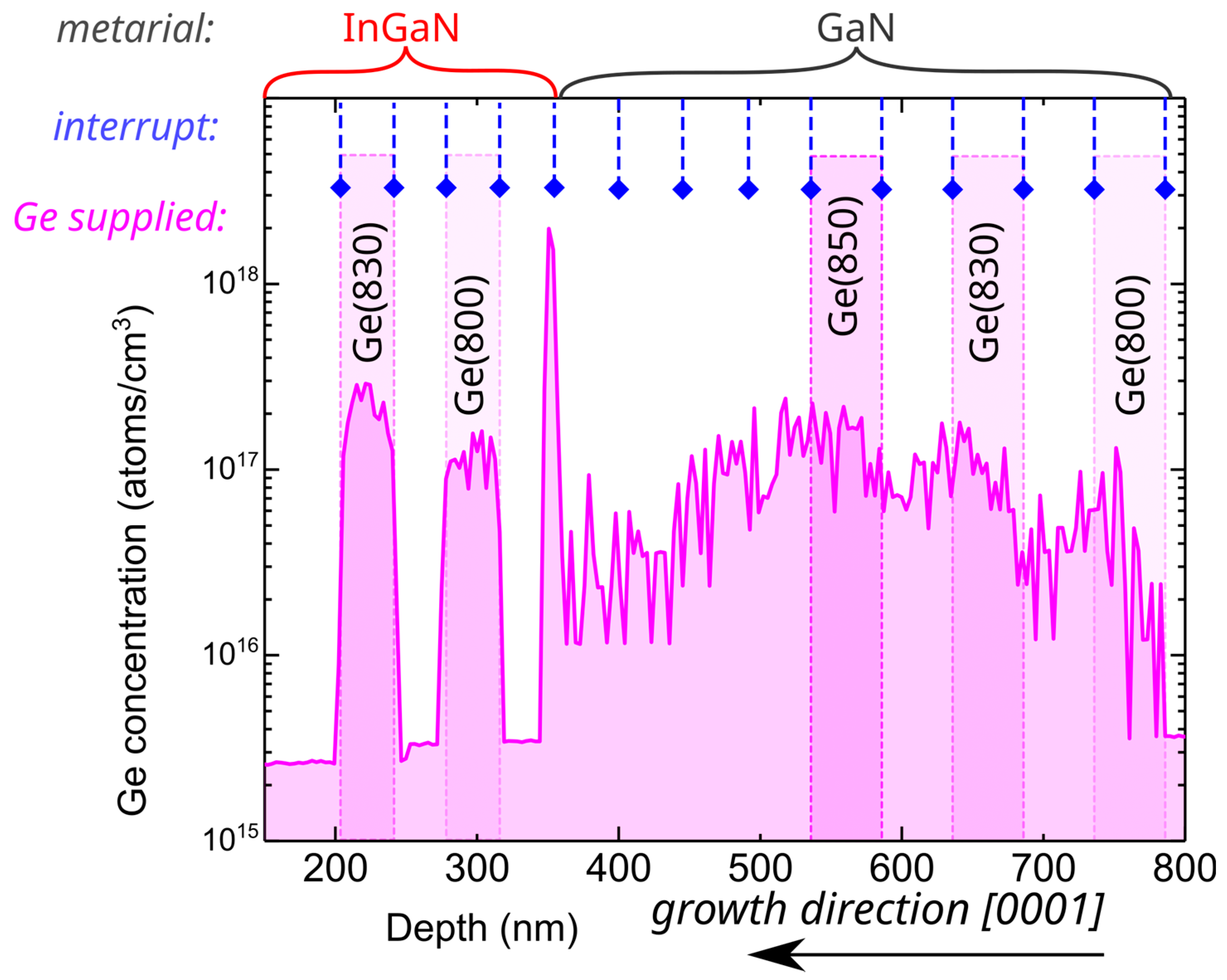
We started the investigation by comparing doping profiles for GaN and InGaN layers grown using relatively low germanium fluxes obtained using a Ge effusion cell set to temperatures between 800 °C and 850 °C. For GaN:Ge grown at substrate temperature of 730 °C under Ga-rich conditions, this resulted in a Ge concentration between
and
. Growth was periodically interrupted for 30–60 s to allow for metal (Ga or In) excess desorption, as depicted in
Figure 1 by dashed lines with blue diamonds. To resolve the abruptness of the doping profile, GaN layers doped with different germanium fluxes were separated with layers that were intentionally grown with the germanium cell closed (Ge was not supplied). In spite of the fact that the Ge shutter was closed, the Ge concentration in GaN, depicted on the right-hand side of
Figure 1, showed no abrupt change in Ge concentration, and the obtained profile was rather dissolved. Interfaces between GaN:Ge and undoped GaN layers, which are fingerprints of the “memory effect” that is manifested as a relatively high unintentional doping level persisting after closing of the dopant source, were very hard to identify. This could indicate that Ge can be either dissolved in a metallic Ga adlayer or can float on top of it. At the depth of 350 nm (
Figure 1), the growth temperature was lowered to 650 °C, to ensure the optimal temperature for the use of indium as a surfactant, and InGaN growth started. First, a 30 nm-thick layer (depth 320–350 nm) was grown with no Ge supplied. Then, two InGaN:Ge layers utilizing different Ge cell temperatures were grown. Between doped layers, we used the undoped layer to resolve the abruptness of the doping profile.
Contrary to GaN growth, for InGaN the Ge doping profile presented in
Figure 1 is sharp and, as desired, all Ge atoms were incorporated into the crystal rather than remaining dissolved in the metallic adlayer. Moreover, as can be deduced from the sharp peak in Ge concentration near the depth of 350 nm in
Figure 1, all Ge atoms accumulated on the surface during GaN:Ge growth (depths 780–530 nm), causing the substantial background doping at depths between 530 and 350 nm, and became incorporated immediately as the growth of InGaN layer started.
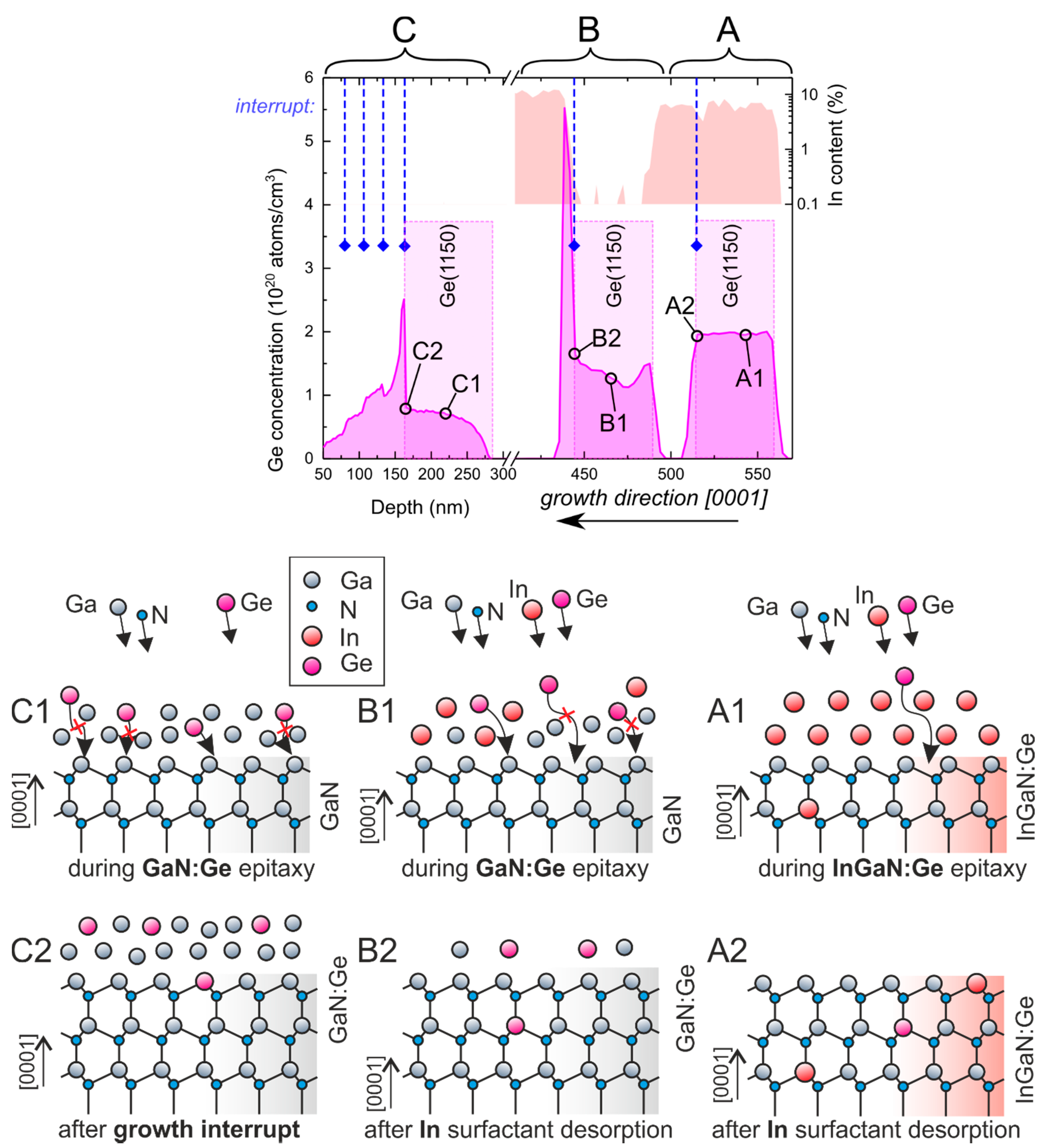
To explicitly present the difference in Ge incorporation into InGaN and GaN layers, a structure comprising three layers, A, B and C, was grown at the same temperature (650 °C), constant growth rate (0.85 µm/h), as defined by RF plasma parameters, and Ge flux, as defined by the constant Ge cell temperature (1150 °C), but with varying surfactants (In or Ga) and Ga/N flux ratios. Layers A, B and C were InGaN with In as the surfactant, GaN with In as the surfactant, and GaN with Ga as the surfactant, respectively. The type of metallic adlayer and Ga/N ratio for each of the doped and capping layers are listed in
Table 1. Resulting Ge and In compositions are presented on the left-hand side of
Figure 2. In each case, the doped layer continuously grew, with an interruption at the end, followed by the growth of an intentionally undoped layer. Schematic images of the surface and metal adlayers are presented on the right-hand side of
Figure 2 labeled corresponding to markers included in the SIMS profile.
For layer “A”, indium was used as a surfactant, and a gallium flux lower than the nitrogen flux was used to enable indium incorporation into the layer [
28]. At such conditions, all Ga and Ge atoms were incorporated during growth (as schematically depicted in (A1)), so after the growth interruption (A2), when undoped growth resumed, Ge concentration dropped sharply and indium composition stayed constant, as depicted in layer “A” in
Figure 2. The noticeably smaller indium content right next to the growth interruption (to about 5% or so) was most probably caused by a gallium cell transient.
For layer “B”, indium was also used as a surfactant, but the gallium flux was slightly higher than the nitrogen flux, resulting in negligible indium incorporation and accumulation of gallium on the surface [
28]. This led to the situation where not all Ga and Ge atoms were incorporated during growth (B1), and after the interruption, only excess indium could be desorbed (B2). This point is indicated by a dashed line and diamond. When growth was resumed, using similar fluxes as for section “A”, first, accumulated Ga became incorporated, and soon afterwards indium composition jumped from ≈ 0 to about 10%. When excess gallium became incorporated, all Ge atoms that were not built into the crystal during the growth of the doped part became immediately incorporated, causing a spike in Ge concentration near (B2). The total (integrated) amount of Ge detected by SIMS in “A” and “B” was the same, within a 2% discrepancy, which points to negligible Ge desorption at the used growth temperature.
For layer “C”, no indium was introduced during growth (C1). Instead, the gallium flux was set to be about 10% higher than the nitrogen flux to ensure gallium accumulation, leading to the formation of the gallium wetting layer. This resulted in significantly lower germanium incorporation throughout the doped layer. After the intentionally doped part, 30 s interruptions were introduced every 25 nm of further growth of intentionally undoped GaN. As shown in
Figure 2, in layer “C”, each interface could be clearly resolved as it was accompanied by a steep change in germanium concentration. Even after four periods of 25 nm-thick GaN layers, with no extra Ge introduced, the germanium dissolved in gallium present on the surface (C2) behaved as a dopant reservoir, provoking Ge doping at the level of
.
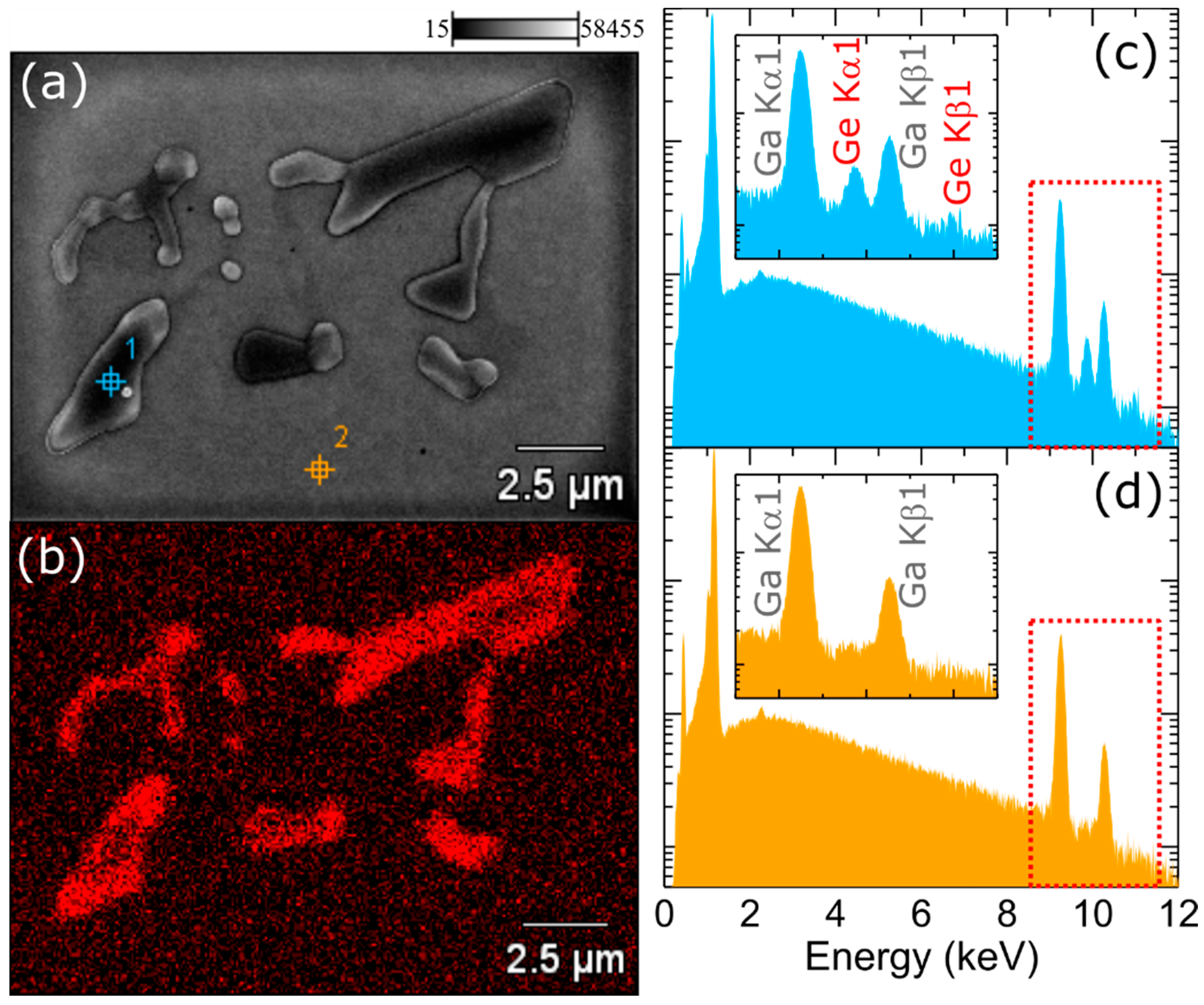
To further analyze what is happening with germanium atoms that do not incorporate into GaN crystal, but stay at the surface, we investigated the surface of the 500 nm-thick, continuously doped GaN:Ge layer using an SEM setup equipped with EDX. The layer was grown using the same Ge flux as for layers presented in
Figure 2. The surface after growth was decorated with crystallites, which were also visible under an optical microscope. A typical SEM image is presented in
Figure 3a. The crystallites exhibited clear crystallographic 3-fold symmetry. The elemental distribution map (
Figure 3b) confirmed that these crystallites are extremely Ge-rich. EDX spectra for crystallite and away from crystallite are compared in
Figure 3c,d, respectively. Since the layer was grown at about 730 °C and under excess gallium, which was desorbed after growth, we concluded that these crystallites were most likely pure germanium crystals that were grown from solution in the liquid gallium.
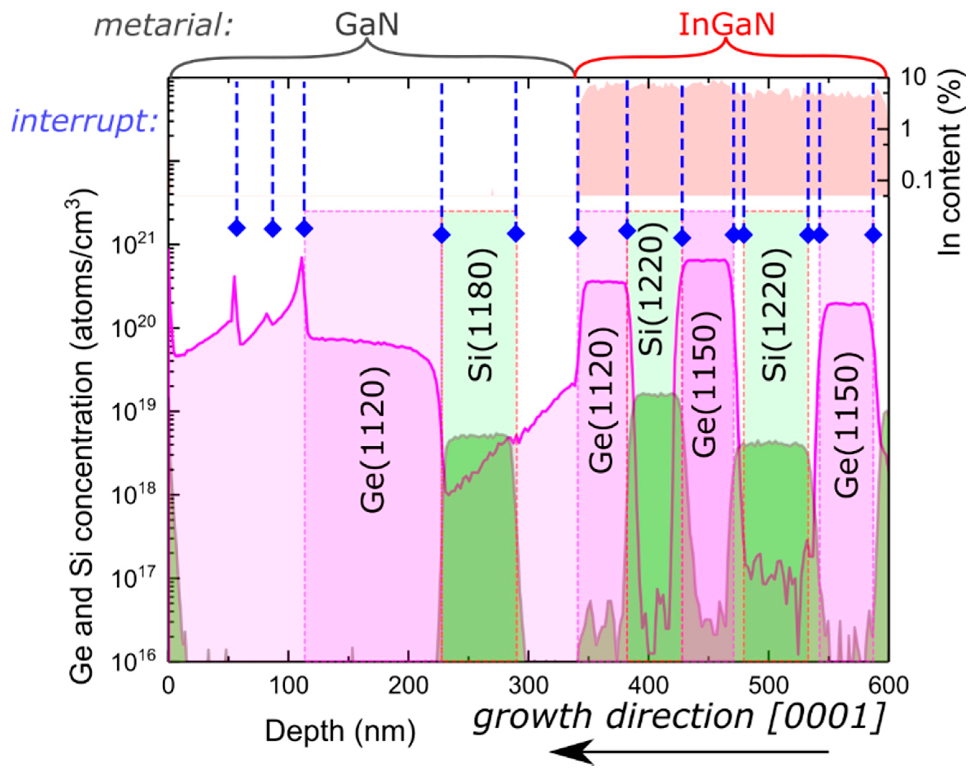
Finally, to compare the results presented above for germanium with silicon, which is most commonly used for
n-type dopants, we grew a SIMS stack where both dopants were used. This allowed for the direct presentation of different behaviors for Si and Ge dopants, in the same sample and under equivalent conditions. Layers utilizing different dopants were alternated as depicted in the SIMS profile presented in
Figure 4. To prove that the observed peculiarity for Ge-doped layers occurred in a wide spectrum of growth conditions, first, two InGaN layers (depth 600–470 nm) were grown at a growth rate of 0.85 µm/h and later (between 470 and 340 nm) at 0.35 µm/h. The growth rate was controlled using the nitrogen flux. The temperature of Si and Ge effusion cells was changed between layers to match the values indicated in
Figure 4. The highest Ge concentration was obtained for Ge effusion cell temperature of 1150 °C and a growth rate of 0.35 µm/h used in InGaN, which resulted in a Ge concentration of
. No difference in sharpness of the profiles between Si and Ge in InGaN was obtained.
Near the depth of 340 nm, the growth temperature was increased to allow for desorption of the gallium excess. Further growth was conducted in Ga-rich conditions without introducing In. Contradictory to the Ge peak observed for the transition from GaN to InGaN growth present near 350 nm in
Figure 1, for the transition from InGaN to GaN, high doping background in intentionally undoped GaN was obtained (depth 340–225 nm in
Figure 4). The doping background decreased from
(near 340 nm) to
(at 225 nm), which might indicate the presence of a finite Ge reservoir at the surface. Between the depths 225 and 340 nm, for reference with Ge doping, intentional Si was introduced during growth. In the case of Si, the doping profiles shown in
Figure 4 were very sharp. No difference between growth under the Ga and In excess for Si doping was found. Between the depths of 110–225 nm, Ge was intentionally introduced during growth in the same conditions as those used in the Si-doped layer proceeding it.
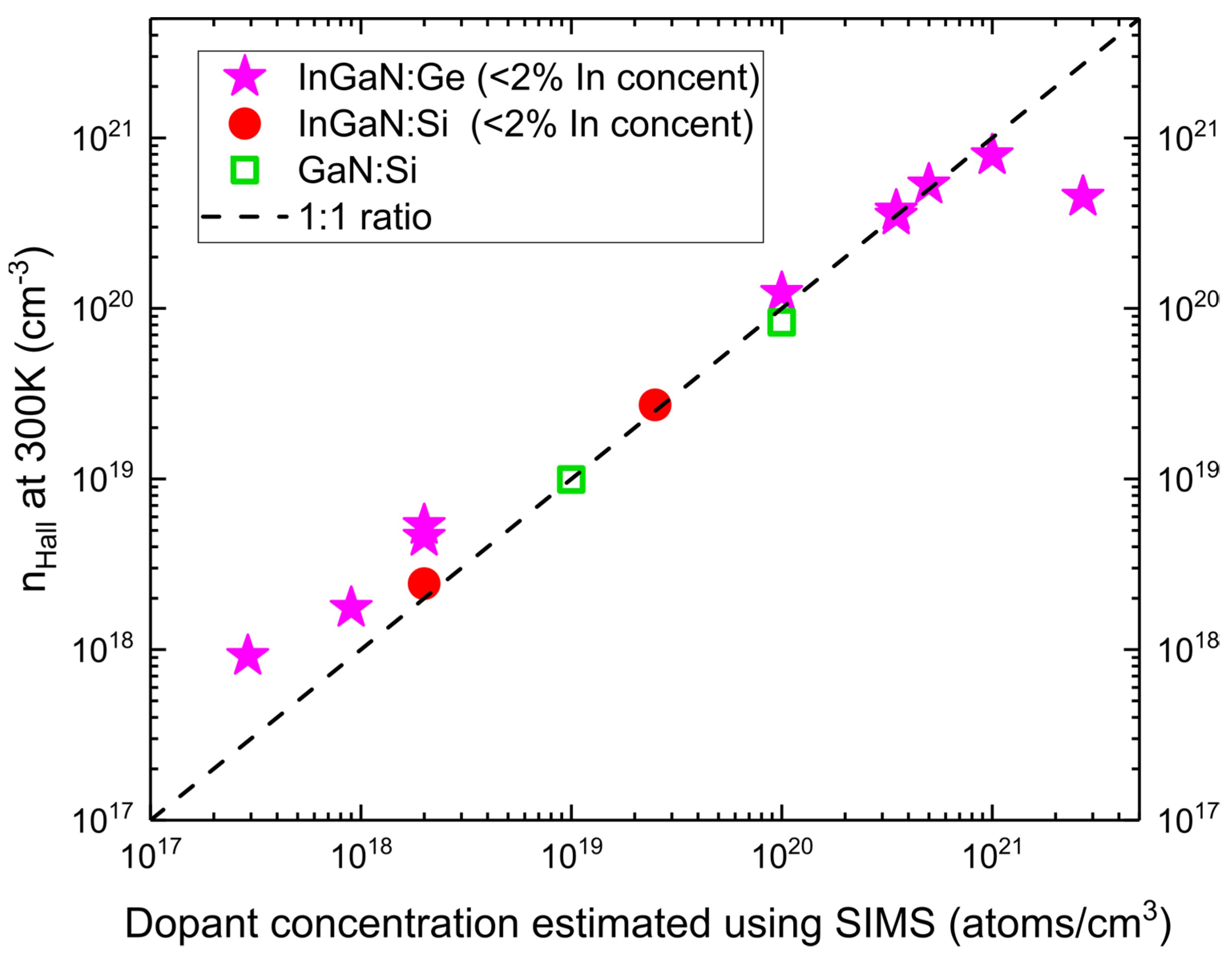
Concerning the electrical activity of introduced dopant, using the indium wetting layer, we obtained low-indium-content InGaN:Ge layer with one of the highest reported electron concentrations (n
Hall) in
n-type doped nitrides reaching
as obtained by Hall measurement [
29]. n
Hall for InGaN:Ge, together with InGaN:Si and GaN:Si samples for reference, as a function of dopant concentrations estimated by SIMS, are presented in
Figure 5. In the wide doping range of interest, from
to
, the concentration of the free carriers corresponded exactly to the number of the introduced dopants as estimated by SIMS. The highest concentration of germanium obtained by SIMS in InGaN:Ge samples was close to
, which was limited by the used Ge flux. In that case, electron concentration was lower:
. The presented dependence of n
Hall versus dopant concentration suggests that Ge incorporation occurs dominantly in donor sites up to concentrations around
Differences between Ge and Si in n
Hall at low doping concentrations are most probably caused by lower accuracy of flux extrapolation in that range.
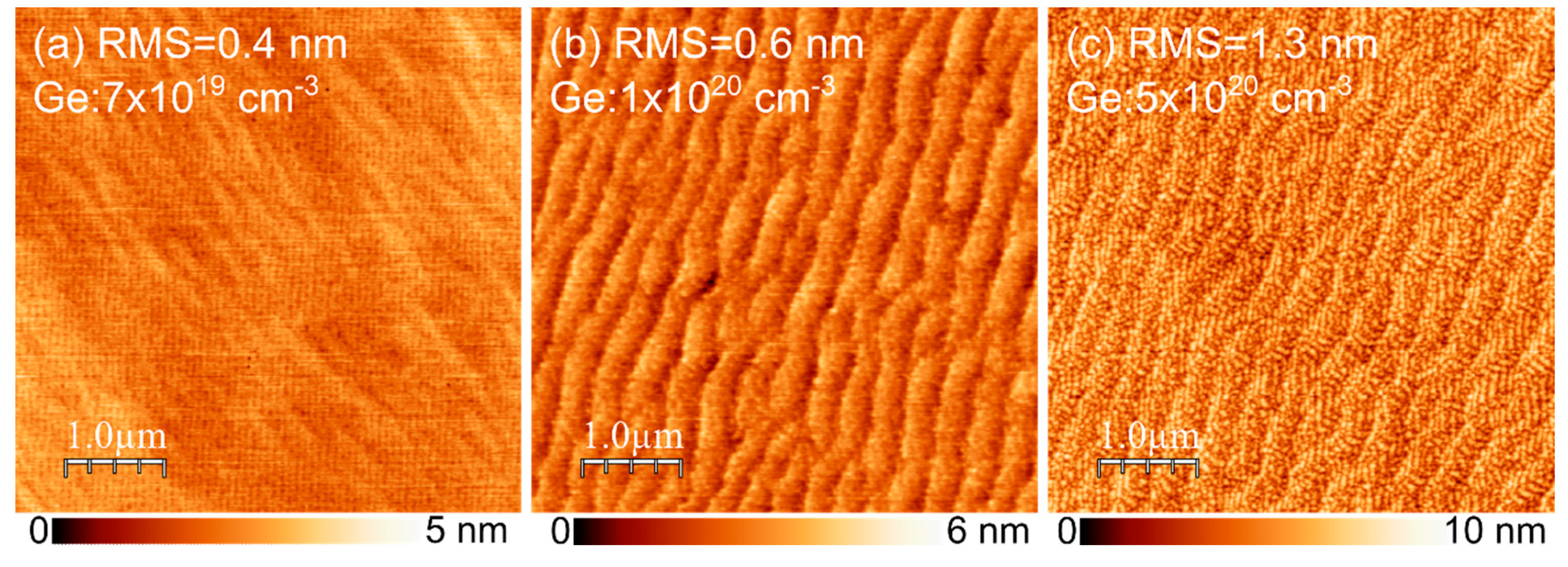
The InGaN:Ge morphology was also investigated as a function of Ge doping to assess its quality. In this case, 30 nm-thick InGaN:Ge layers with no cap were grown on 100 nm GaN buffer using different Ge cell temperatures. The resulting morphologies are presented in
Figure 6. The root mean square (RMS) value increased with increasing germanium concentration, which, at least to some extent, can be engineered by further optimization of the main heater correction needed due to the change in surface temperature caused by a significant change in absorption [
16]. Atomic steps could be clearly resolved up to
. At this level, atomic steps started to be wavy. Adding even more Ge resulted in higher roughness that might have been due to the postulated effect of Ge atoms on the mobility of Ga atoms [
30].
4. Discussion
Previous reports on the limitations of Ge doping level during GaN growth investigated the restrictions imposed by the crystal itself. This study showed that the state of the surface during the growth, especially the type of surfactant metal, can be more discriminative towards dopant incorporation than the crystal itself. Presented experimental results indicate pronounced difficulties in obtaining high Ge concentrations in GaN grown under Ga-rich conditions, typical for plasma-assisted MBE. It is important to note that the observed “memory effect”, caused by Ge atoms accumulating or dissolving in the Ga adlayer, was also present for relatively low doping concentrations, as presented in
Figure 1. The “memory effect”, if not properly managed, will have even more severe repercussions on the growth of heavily doped heterostructures, such as tunnel junctions, where precise control of doping profiles and interfaces determines the device performance. For thick, heavily doped GaN:Ge layers, it also leads to Ge precipitates, as reported before by others [
25] and observed also for our crystals.
In the literature, the presence of a limiting mechanism for Ge incorporation into GaN is supported by reports of the use of Ge as a catalyst for the growth of GaN nanowires (NWs) [
31]. In that study, Ge deposited onto Si surface prior to growth formed droplets that catalyze NW growth and lead to relatively small (~10
19 ) germanium contamination [
32].
The doping profiles and incorporation of Ge atoms into nitride layers completely changed when Ga is replaced by an In adlayer. In the case indium was used as a surfactant, all impinging Ge was incorporated into the crystal rather than staying at the surface. This change was strictly associated with the element used as a metallic surfactant. It can be concluded from the fact that growth at the same temperature for the Ga surfactant led to a pronounced “memory effect” in the composition profile in contrast to the In-surfactant that facilitated abrupt doping interfaces. Importantly, such an effect was not expected judging from solubility diagrams for Ge in Ga and In. Both elements offer high solubility, with a slightly higher value for Ga (55%) than for In (45%).
Furthermore, no difference between doping profiles for the Ga and In adlayer for the Si-doped III-nitride layers was obtained. No “memory effect” or dissolved interfaces present for Ge-doped layers were observed for this Si profile.
The most plausible cause for distinct incorporation mechanisms for Ge and Si atoms for different kinds of adlayers is the alteration in diffusivity of the dopants. This, in turn, might be connected with the relative size of the atoms. Since the Ge atom is slightly larger than the Ga atom, the dopant diffusing through an organized Ga adlayer is blocked. For the much smaller Si atom, the same adlayer might not present a significant diffusion barrier. The In adlayer, on the other hand, consists of atoms larger than Ge, which could explain why Ge, in this case, can more easily diffuse through it, resulting in the sharp doping profiles and the lack of “memory effect” observed in that case.


 ,
, 


