
CVD Nanocrystalline Diamond Film Doped with Eu

 , ,
, , 
Abstract
:1. Introduction
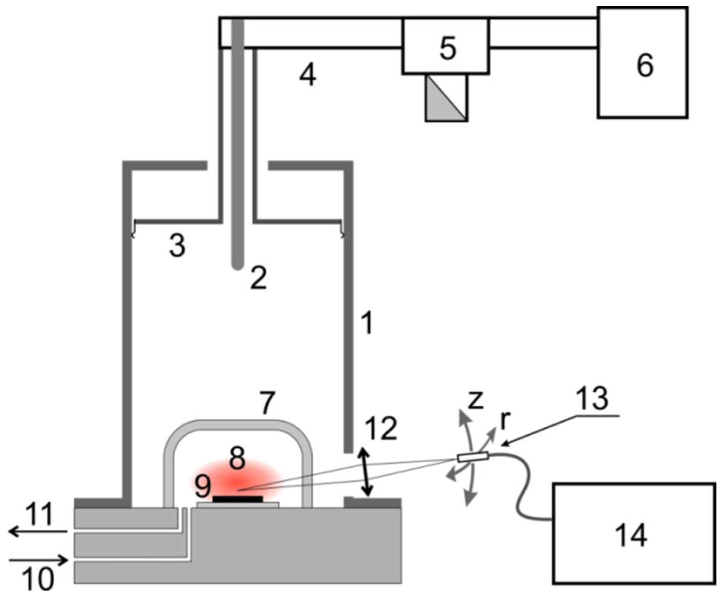
2. Materials and Methods
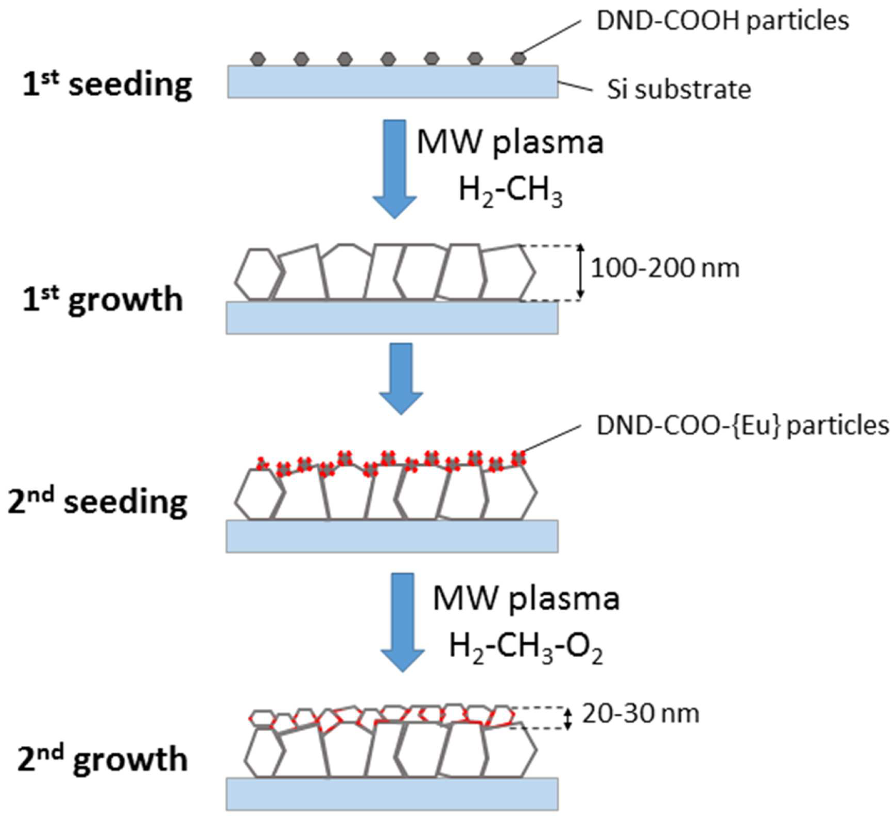
- The first stage was the seeding of a silicon substrate with diamond powder using a DND suspension (conc. 0.69 wt.%). The DND hydrosol was sonicated for two hours. All silicon substrates were preliminarily cleaned in acetone in an ultrasonic bath, then ultrasonicated in hydrosol for two hours.
- The products from the first stage of growing a silicon substrate were placed in a CVD reactor. DND particles acted as nucleation centers during the growth of a nanocrystalline diamond film. The duration of the diamond film growth process was one hour; as a result of the growth, the film thickness was 300 nm. The film thickness was measured by the method described in the previous paper [12].
- In the second stage, the surface of nanocrystalline diamond film was treated with nanodiamond particles with a surface modified with Eu ions. The concentration of the DND-Eu particles in hydrosol was 1.43 wt.%.
- Then, in the second stage, growth of a diamond film on DND-Eu particles was completed. The overgrowth time was 10 min and the thickness of diamond film doped with Eu did not exceed 50 nm.
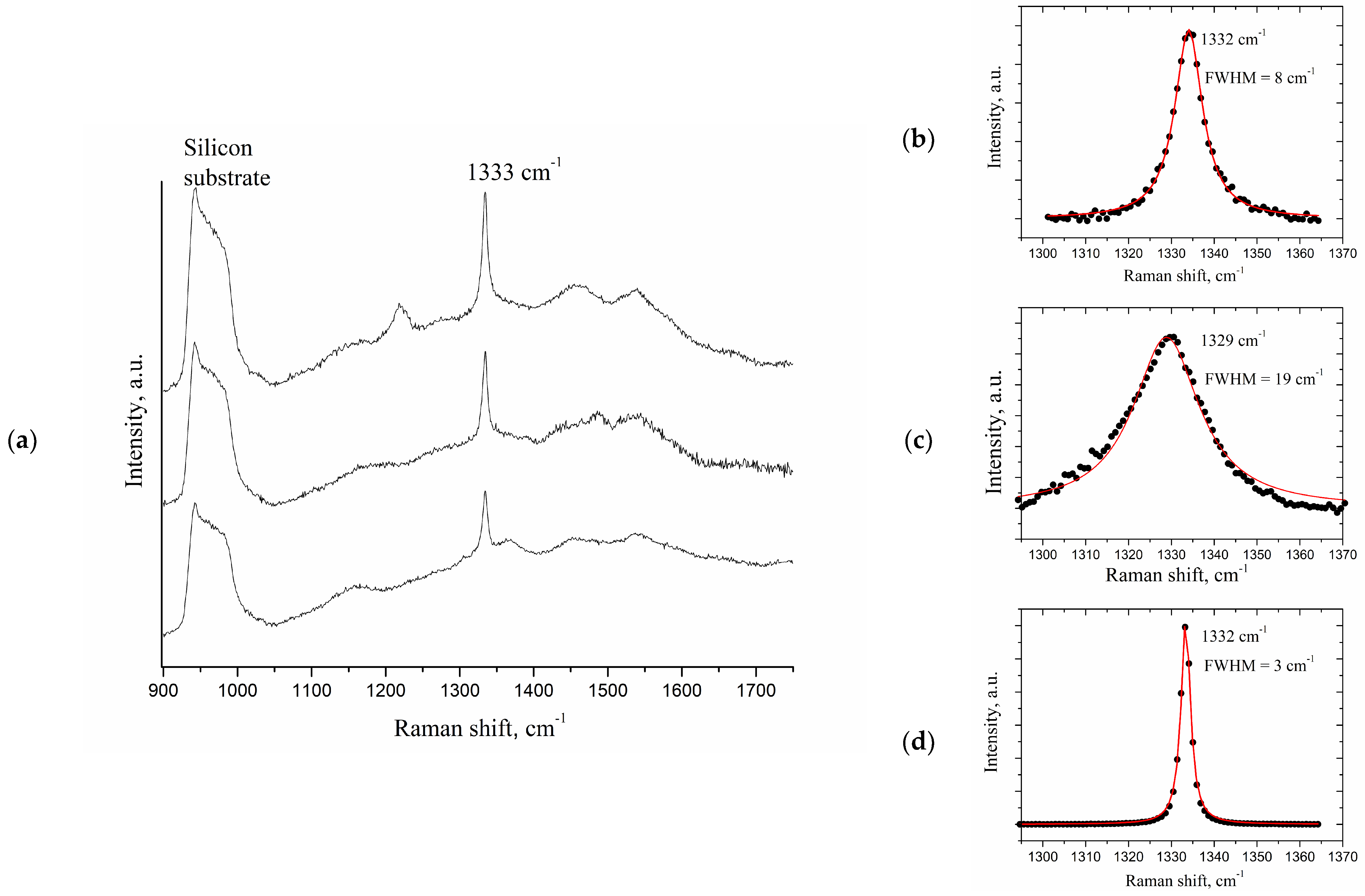
3. Results and Discussion
4. Conclusions
Author Contributions
Funding
Institutional Review Board Statement
Informed Consent Statement
Data Availability Statement
Acknowledgments
Conflicts of Interest
References
- Koizumi, S.; Umezawa, H.; Pernot, J.; Suzuki, M. Power Electronics Device Applications of Diamond Semiconductors, 1st ed.; Koizumi, S., Umezawa, H., Pernot, J., Suzuki, M., Eds.; Woodhead Publishing: Duxford, UK, 2018. [Google Scholar]
- Tsao, J.Y.; Chowdhury, S.; Hollis, M.A.; Jena, D.; Johnson, N.M.; Jones, K.A.; Kaplar, R.J.; Rajan, S.; Van de Walle, C.G.; Bellotti, E.; et al. Ultrawide-Bandgap Semiconductors: Research Opportunities and Challenges. Adv. Electron. Mater. 2018, 4, 1600501. [Google Scholar] [CrossRef] [Green Version]
- Aharonovich, I.; Castelletto, S.; Simpson, D.A.; Su, C.-H.; Greentree, A.D.; Prawer, S. Diamond-based single-photon emitters. Rep. Prog. Phys. 2011, 74, 076501. [Google Scholar] [CrossRef]
- Bradac, C.; Gao, W.; Forneris, J.; Trusheim, M.E.; Aharonovich, I. Quantum Nanophotonics with Group IV Defects in Diamond. Nat. Commun. 2019, 10, 1–13. [Google Scholar] [CrossRef] [PubMed]
- Magyar, A.; Hu, W.; Shanley, T.; Flatté, M.E.; Hu, E.; Aharonovich, I. Synthesis of Luminescent Europium Defects in Diamond. Nat. Commun. 2014, 5, 1–6. [Google Scholar] [CrossRef] [PubMed] [Green Version]
- Sedov, V.S.; Kuznetsov, S.V.; Ralchenko, V.G.; Mayakova, M.N.; Krivobok, V.S.; Savin, S.S.; Zhuravlev, K.P.; Martyanov, A.K.; Romanishkin, I.D.; Khomich, A.A.; et al. Diamond-EuF3 Nanocomposites with Bright Orange Photoluminescence. Diam. Relat. Mater. 2017, 72, 47–52. [Google Scholar] [CrossRef]
- Qin, S.R.; Zhao, Q.; Cheng, Z.G.; Zhang, D.X.; Zhang, K.K.; Su, L.X.; Fan, H.J.; Wang, Y.H.; Shan, C.X. Rare Earth-Functionalized Nanodiamonds for Dual-Modal Imaging and Drug Delivery. Diam. Relat. Mater. 2019, 91, 173–182. [Google Scholar] [CrossRef]
- Sedov, V.; Kouznetsov, S.; Martyanov, A.; Proydakova, V.; Ralchenko, V.; Khomich, A.; Voronov, V.; Batygov, S.; Kamenskikh, I.; Spassky, D.; et al. Diamond–Rare Earth Composites with Embedded NaGdF4:Eu Nanoparticles as Robust Photo- and X-Ray-Luminescent Materials for Radiation Monitoring Screens. ACS Appl. Nano Mater. 2020, 3, 1324–1331. [Google Scholar] [CrossRef]
- Cajzl, J.; Nekvindová, P.; Macková, A.; Malinský, P.; Oswald, J.; Remeš, Z.; Varga, M.; Kromka, A.; Akhetova, B.; Böttger, R.; et al. Erbium Luminescence Centres in Single- and Nano-Crystalline Diamond-Effects of Ion Implantation Fluence and Thermal Annealing. Micromachines 2018, 9, 316. [Google Scholar] [CrossRef] [PubMed] [Green Version]
- Vul, A.Y.; Shenderova, O.A. Detonation Nanodiamonds—Science and Applications; Vul, A.Y., Shenderova, O.A., Eds.; Pan Stanford Publishing: Singapore, 2013. [Google Scholar] [CrossRef]
- Arnault, J.C. Nanodiamonds: Advanced Material Analysis, Properties and Applications; Arnault, J.-C., Ed.; Elsevier Inc.: Amsterdam, The Netherlands, 2017. [Google Scholar] [CrossRef]
- Vikharev, A.L.; Bogdanov, S.A.; Ovechkin, N.M.; Ivanov, O.A.; Radishev, D.B.; Gorbachev, A.M.; Lobaev, M.A.; Vul, A.Y.; Dideikin, A.T.; Kraev, S.A.; et al. Study of Undoped Nanocrystalline Diamond Films Grown by Microwave Plasma-Assisted Chemical Vapor Deposition. Semiconductors 2021, 55, 66–75. [Google Scholar] [CrossRef]
- Yudina, E.B.; Aleksenskii, A.E.; Fomina, I.G.; Shvidchenko, A.V.; Danilovich, D.P.; Eremenko, I.L.; Vul, A.Y. Interaction of Carboxyl Groups with Rare Metal Ions on the Surface of Detonation Nanodiamonds. Eur. J. Inorg. Chem. 2019, 2019, 4345–4349. [Google Scholar] [CrossRef]
- Vanpoucke, D.E.P.; Nicley, S.S.; Raymakers, J.; Maes, W.; Haenen, K. Can Europium Atoms Form Luminescent Centres in Diamond: A Combined Theoretical–Experimental Study. Diam. Relat. Mater. 2019, 94, 233–241. [Google Scholar] [CrossRef] [Green Version]
- Bogdanov, S.A.; Gorbachev, A.M.; Vikharev, A.L.; Radishev, D.B.; Lobaev, M.A. Study of Microwave Discharge at High Power Density Conditions in Diamond Chemical Vapor Deposition Reactor by Optical Emission Spectroscopy. Diam. Relat. Mater. 2019, 97, 107407. [Google Scholar] [CrossRef]
- Williams, O.A.; Nesládek, M.; Mareš, J.J.; Hubík, P. Growth and Properties of Nanocrystalline Diamond Films. In Physics and Applications of CVD Diamond; Koizumi, S., Nebel, C., Nesladek, M., Eds.; WILEY-VCH Verlag GmbH & Co. KGaA: Weinheim, Germany, 2008; pp. 13–26. [Google Scholar]
- Naamoun, M.; Tallaire, A.; Silva, F.; Achard, J.; Doppelt, P.; Gicquel, A. Etch-Pit Formation Mechanism Induced on HPHT and CVD Diamond Single Crystals by H2/O2 Plasma Etching Treatment. Phys. Status Solidi 2012, 209, 1715–1720. [Google Scholar] [CrossRef]
- Dideikin, A.T.; Aleksenskii, A.E.; Baidakova, M.V.; Brunkov, P.N.; Brzhezinskaya, M.; Davydov, V.Y.; Levitskii, V.S.; Kidalov, S.V.; Kukushkina, Y.A.; Kirilenko, D.A.; et al. Rehybridization of Carbon on Facets of Detonation Diamond Nanocrystals and Forming Hydrosols of Individual Particles. Carbon 2017, 122, 737–745. [Google Scholar] [CrossRef]
- Meilakhs, A.P.; Koniakhin, S.V. New Explanation of Raman Peak Redshift in Nanoparticles. Superlattices Microstruct. 2017, 110, 319–323. [Google Scholar] [CrossRef] [Green Version]
- Baidakova, M.V.; Vul’, A.Y.; Golubev, V.G.; Grudinkin, S.A.; Melekhin, V.G.; Feoktistov, N.A.; Krüger, A. Growth of Diamond Films on Crystalline Silicon by Hot-Filament Chemical Vapor Deposition. Semiconductors 2002, 36, 615–620. [Google Scholar] [CrossRef]


Publisher’s Note: MDPI stays neutral with regard to jurisdictional claims in published maps and institutional affiliations. |
© 2022 by the authors. Licensee MDPI, Basel, Switzerland. This article is an open access article distributed under the terms and conditions of the Creative Commons Attribution (CC BY) license (https://creativecommons.org/licenses/by/4.0/).
Share and Cite
Yudina, E.B.; Aleksenskii, A.E.; Bogdanov, S.A.; Bukalov, S.S.; Leites, L.A.; Radishev, D.B.; Vikharev, A.L.; Vul’, A.Y. CVD Nanocrystalline Diamond Film Doped with Eu. Materials 2022, 15, 5788. https://doi.org/10.3390/ma15165788
Yudina EB, Aleksenskii AE, Bogdanov SA, Bukalov SS, Leites LA, Radishev DB, Vikharev AL, Vul’ AY. CVD Nanocrystalline Diamond Film Doped with Eu. Materials. 2022; 15(16):5788. https://doi.org/10.3390/ma15165788
Chicago/Turabian StyleYudina, Elena B., Alexander E. Aleksenskii, Sergey A. Bogdanov, Sergey S. Bukalov, Larisa A. Leites, Dmitry B. Radishev, Anatoly L. Vikharev, and Alexander Y. Vul’. 2022. "CVD Nanocrystalline Diamond Film Doped with Eu" Materials 15, no. 16: 5788. https://doi.org/10.3390/ma15165788
APA StyleYudina, E. B., Aleksenskii, A. E., Bogdanov, S. A., Bukalov, S. S., Leites, L. A., Radishev, D. B., Vikharev, A. L., & Vul’, A. Y. (2022). CVD Nanocrystalline Diamond Film Doped with Eu. Materials, 15(16), 5788. https://doi.org/10.3390/ma15165788