
Surface Morphology Evolution during Chemical Mechanical Polishing Based on Microscale Material Removal Modeling for Monocrystalline Silicon

Abstract
:1. Introduction
2. Micropolishing Model
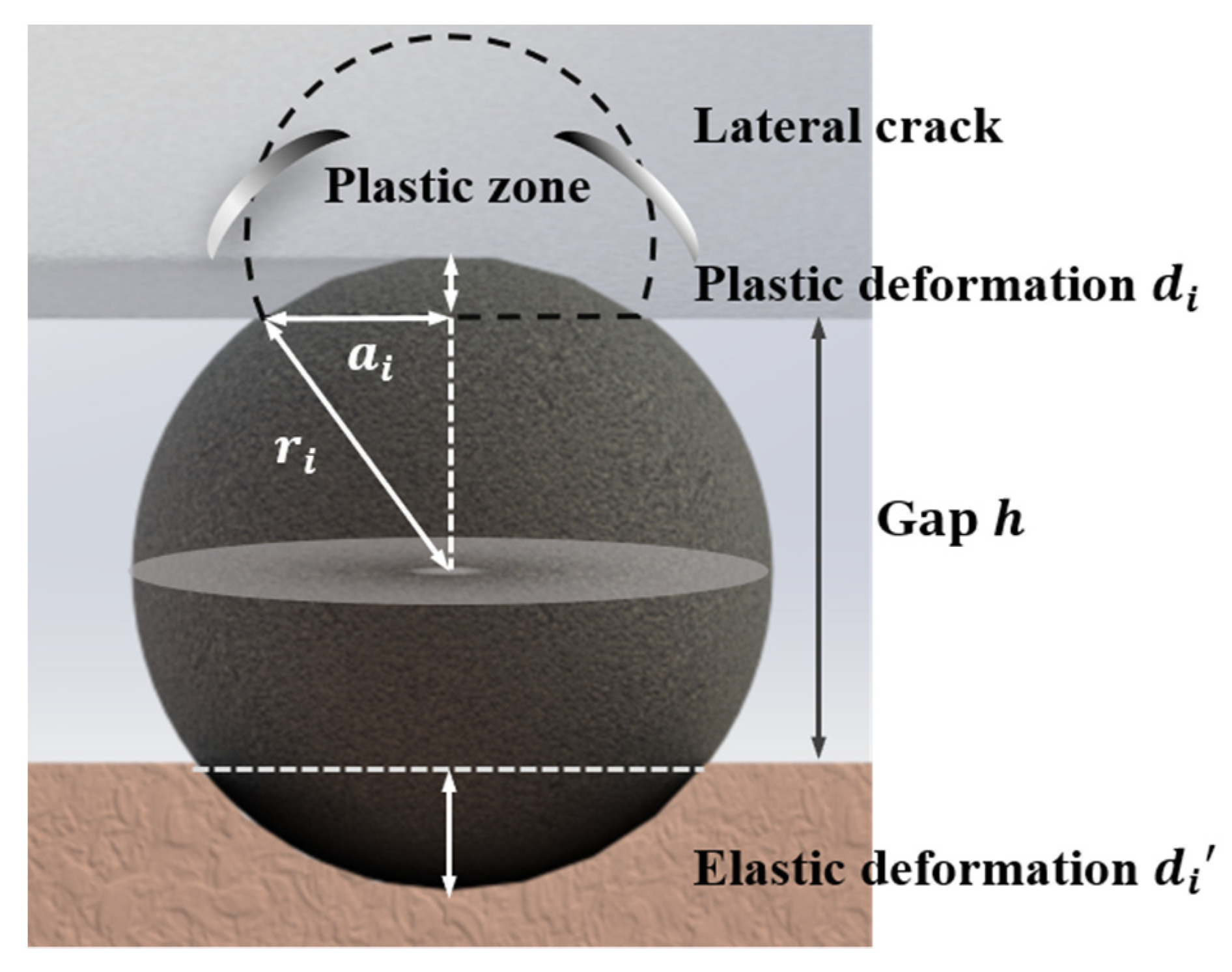
2.1. Mechanical Material Removal by Plastic Deformation
2.2. Chemical Material Removal by Simplified Wet Chemical Etching
2.3. Micropolishing Model during CMP
3. Experimental Setup
4. Results and Discussion
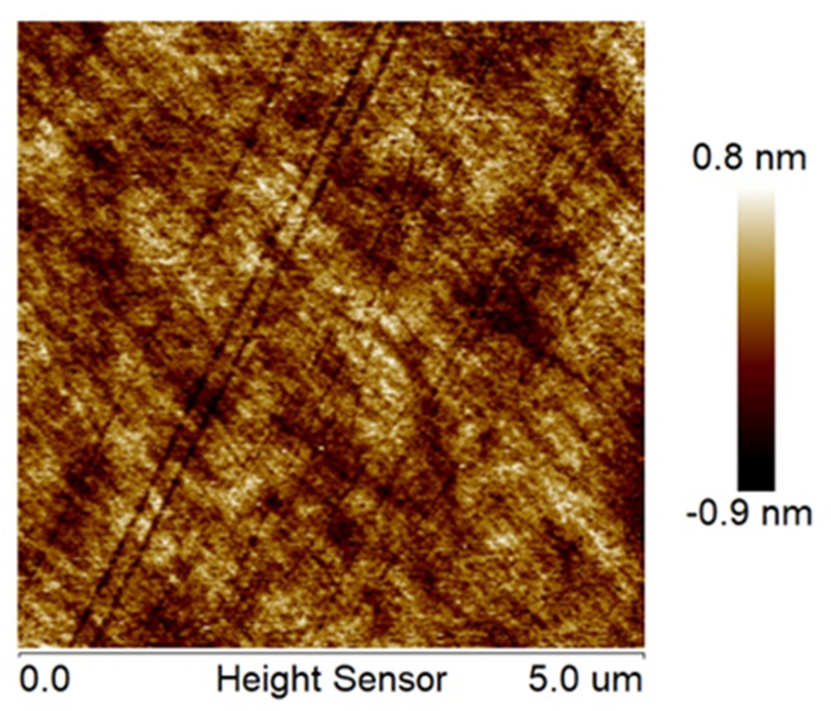
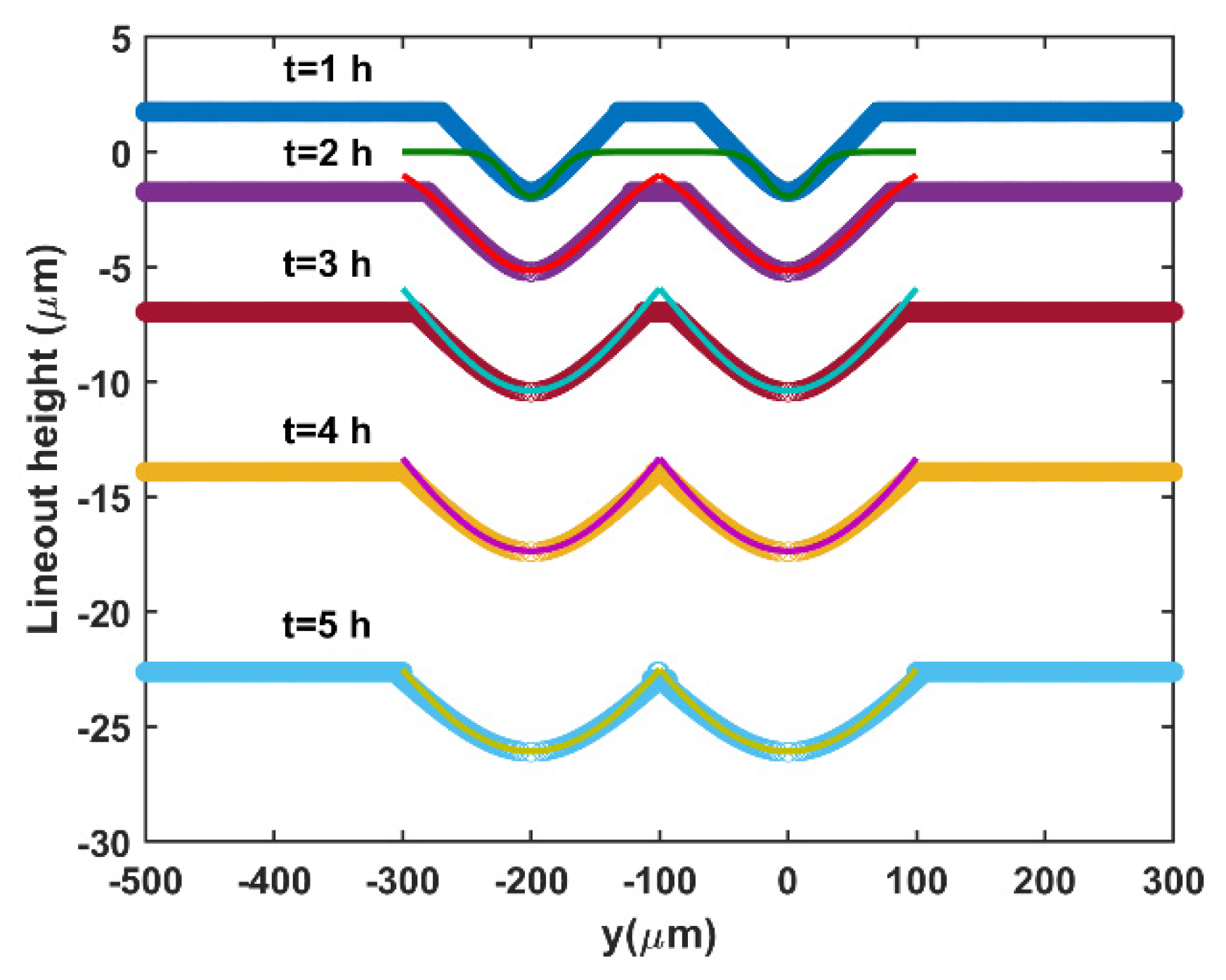
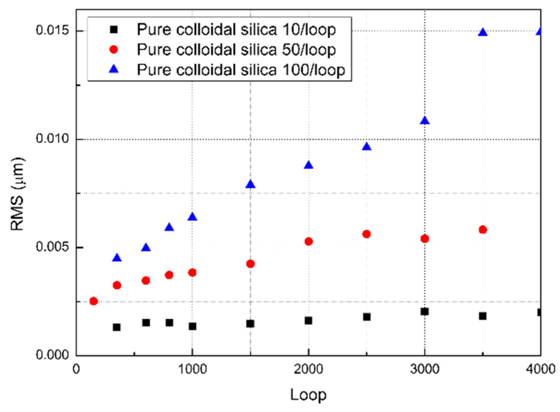
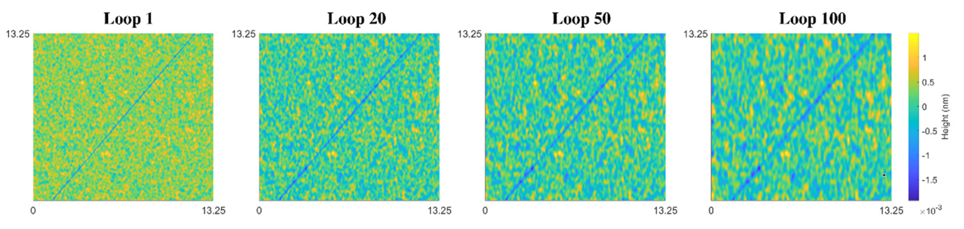
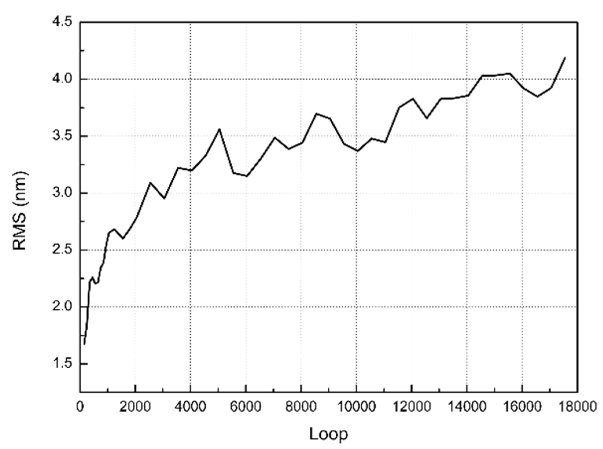
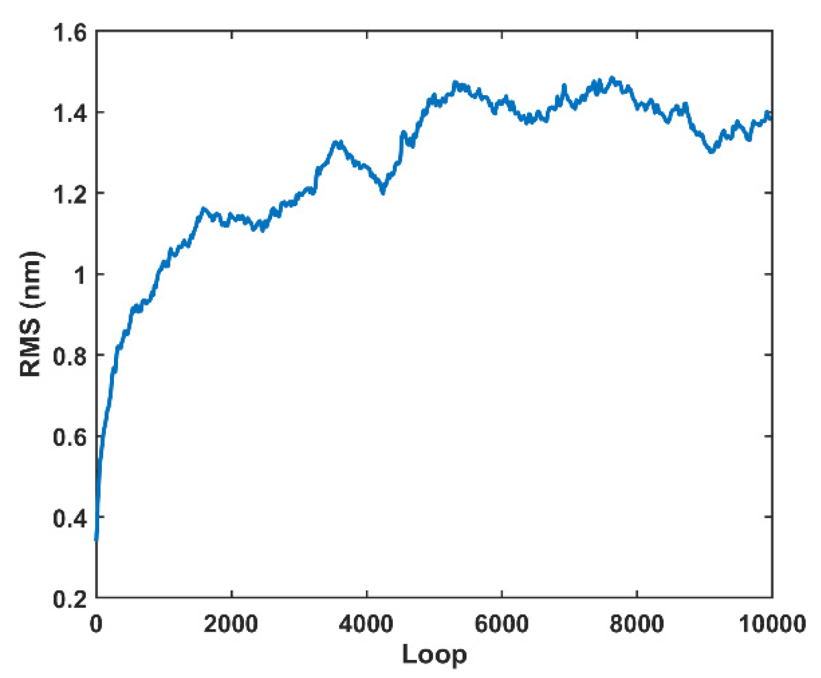
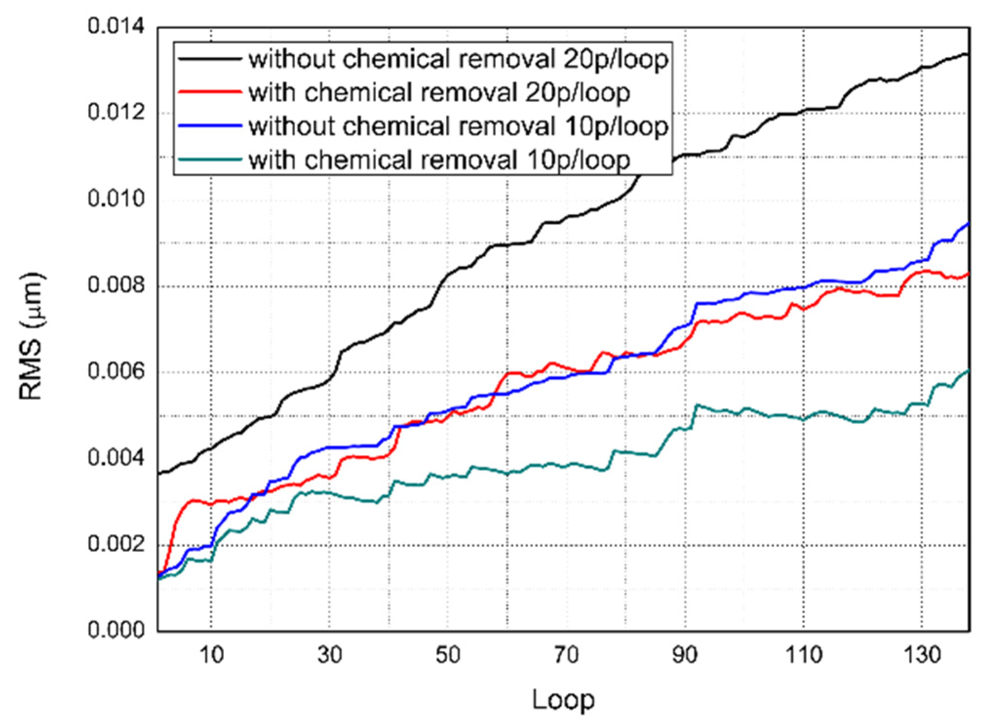
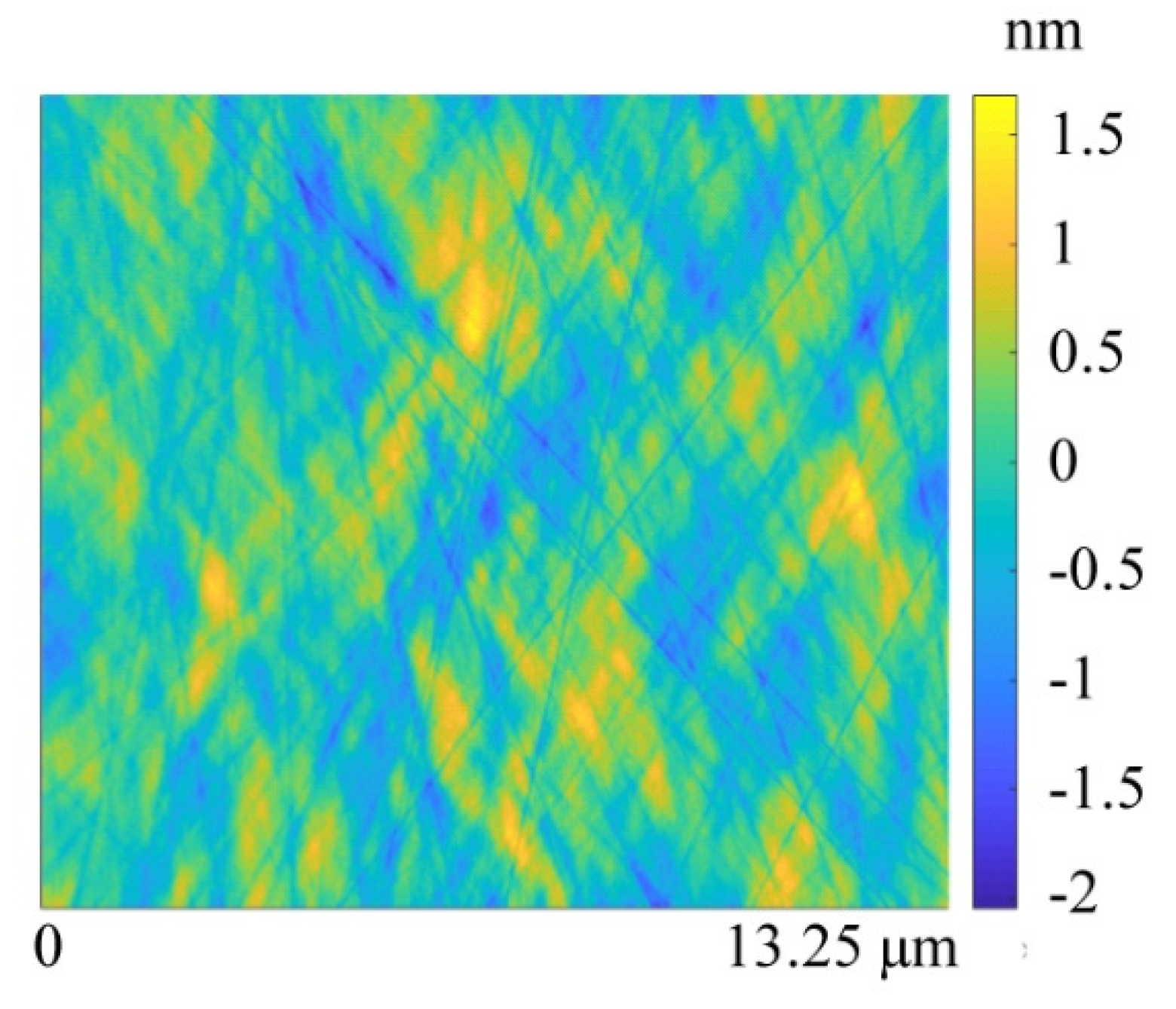
4.1. Verification of the Micropolishing Model and Surface Morphology Evolution
4.2. Engineering Application of the Model
5. Conclusions
Author Contributions
Funding
Institutional Review Board Statement
Informed Consent Statement
Data Availability Statement
Conflicts of Interest
References
- Jiang, B.C.; Zhao, D.W.; Wang, B.Q.; Zhao, H.J.; Liu, Y.H.; Lu, X.C. Flatness Maintenance and Roughness Reduction of Silicon Mirror in Chemical Mechanical Polishing Process. Sci. China Technol. Sci. 2020, 63, 166–172. [Google Scholar] [CrossRef]
- Wang, Z.; Wu, L.; Dun, A.; Fang, Y.; Song, L.; Zhu, X. Research on Ultra-Smooth Machining Technique for Monocrystalline Silicon Substrate. J. Mod. Opt. 2020, 67, 1227–1232. [Google Scholar] [CrossRef]
- Beaucamp, A.; Takizawa, K.; Han, Y.; Zhu, W. Reduction of Mid-Spatial Frequency Errors on Aspheric and Freeform Optics by Circular-Random Path Polishing. Opt. Express 2021, 29, 29802. [Google Scholar] [CrossRef] [PubMed]
- Seo, J. A Review on Chemical and Mechanical Phenomena at the Wafer Interface during Chemical Mechanical Planarization. J. Mater. Res. 2021, 36, 235–257. [Google Scholar] [CrossRef]
- Zhou, G.; Tian, Y.; Xue, S.; Zhou, G.; Song, C.; Zhou, L.; Tie, G.; Shi, F.; Shen, Y.; Zhu, Z. Enhancement of the Load Capacity of High-Energy Laser Monocrystalline Silicon Reflector Based on the Selection of Surface Lattice Defects. Materials 2020, 13, 4172. [Google Scholar] [CrossRef]
- Runnels, S.R. Feature-Scale Fluid-Based Erosion Modeling for Chemical-Mechanical Polishing. J. Electrochem. Soc. 1994, 141, 1900–1904. [Google Scholar] [CrossRef]
- Sundararajan, S.; Thakurta, D.G.; Schwendeman, D.W.; Murarka, S.P.; Gill, W.N. Two-Dimensional Wafer-Scale Chemical Mechanical Planarization Models Based on Lubrication Theory and Mass Transport. J. Electrochem. Soc. 1999, 146, 761–766. [Google Scholar] [CrossRef]
- Han, L.; Zhao, H.; Zhang, Q.; Jin, M.; Zhang, L.; Zhang, P. Research on Influences of Contact Force in Chemical Mechanical Polishing (CMP) Process. AIP Adv. 2015, 5, 041305. [Google Scholar] [CrossRef]
- Lee, H.S.; Jeong, H.D.; Dornfeld, D.A. Semi-Empirical Material Removal Rate Distribution Model for SiO2 Chemical Mechanical Polishing (CMP) Processes. Precis. Eng. 2013, 37, 483–490. [Google Scholar] [CrossRef]
- Qin, K.; Moudgil, B.; Park, C.W. A Chemical Mechanical Polishing Model Incorporating Both the Chemical and Mechanical Effects. Thin Solid Film. 2004, 446, 277–286. [Google Scholar] [CrossRef]
- Bin, L.; Junpeng, Z.; Zhong-chen, C.; Jiannan, Z.; Tian, H. Theoretical and Experimental Investigation on Surface Generation and Subsurface Damage in Fixed Abrasive Lapping of Optical Glass. Int. J. Mech. Sci. 2022, 215, 106941. [Google Scholar] [CrossRef]
- Luo, J.; Dornfeld, D.A. Effects of Abrasive Size Distribution in Chemical Mechanical Planarization: Modeling and Verification. IEEE Trans. Semicond. Manuf. 2003, 16, 469–476. [Google Scholar] [CrossRef]
- Luo, J.; Dornfeld, D.A. Material Removal Mechanism in Chemical Mechanical Polishing: Theory and Modeling. IEEE Trans. Semicond. Manuf. 2001, 14, 112–133. [Google Scholar] [CrossRef]
- Suratwala, T.; Feit, M.; Steele, W.; Wong, L.; Shen, N.; Dylla-Spears, R.; Desjardin, R.; Mason, D.; Geraghty, P.; Miller, P.; et al. Microscopic Removal Function and the Relationship between Slurry Particle Size Distribution and Workpiece Roughness during Pad Polishing. J. Am. Ceram. Soc. 2014, 97, 81–91. [Google Scholar] [CrossRef]
- Suratwala, T.I.; Feit, M.D.; Steele, W.A. Toward Deterministic Material Removal and Surface Figure during Fused Silica Pad Polishing. J. Am. Ceram. Soc. 2010, 93, 1326–1340. [Google Scholar] [CrossRef]
- Suratwala, T.; Steele, W.; Feit, M.; Shen, N.; Wong, L.; Dylla-Spears, R.; Desjardin, R.; Elhadj, S.; Miller, P. Relationship between Surface μ-Roughness and Interface Slurry Particle Spatial Distribution during Glass Polishing. J. Am. Ceram. Soc. 2017, 100, 2790–2802. [Google Scholar] [CrossRef]
- Dylla-Spears, R.; Wong, L.; Miller, P.E.; Feit, M.D.; Steele, W.; Suratwala, T. Charged Micelle Halo Mechanism for Agglomeration Reduction in Metal Oxide Particle Based Polishing Slurries. Colloids Surf. A Physicochem. Eng. Asp. 2014, 447, 32–43. [Google Scholar] [CrossRef]
- Akbar, W.; Ertunç, Ö. A Coupled Material Removal Model for Chemical Mechanical Polishing Processes. ECS J. Solid State Sci. Technol. 2021, 10, 104003. [Google Scholar] [CrossRef]
- Akbar, W.; Ertunç, Ö. Model-Based Optimization of CMP Process Parameters for Uniform Material Removal Selectivity in Cu/Barrier Planarization. ECS J. Solid State Sci. Technol. 2022, 11, 024003. [Google Scholar] [CrossRef]
- Lee, H.; Jeong, H. A Wafer-Scale Material Removal Rate Profile Model for Copper Chemical Mechanical Planarization. Int. J. Mach. Tools Manuf. 2011, 51, 395–403. [Google Scholar] [CrossRef]
- Hu, Y.; Shi, D.; Hu, Y.; Zhao, H.; Sun, X. Investigation on the Material Removal and Surface Generation of a Single Crystal SiC Wafer by Ultrasonic Chemical Mechanical Polishing Combined with Ultrasonic Lapping. Materials 2018, 11, 2022. [Google Scholar] [CrossRef] [PubMed]
- Bifano, T.G.; Dow, T.A.; Scattergood, R.O. Ductile-Regime Grinding of Brittle Materials: Experimental Results and The Development of a Model. In Proceedings of the 32nd Annual International Technical Symposium on Optical and Optoelectronic Applied Science and Engineering, San Diego, CA, USA, 15–18 August 1988. [Google Scholar] [CrossRef]
- Dai, H.; Yue, H.; Hu, Y.; Li, P. The Removal Mechanism of Monocrystalline Si in the Process of Double Diamond Abrasive Polishing by Molecular Dynamics Simulation. Tribol. Lett. 2021, 69, 66. [Google Scholar] [CrossRef]
- Johnson, K.L. Contact Mechanics, 1st ed.; Cambridge University Press: Cambridge, UK, 1985; pp. 312–339. ISBN 0521255767. [Google Scholar]
- Lawn, B. Fracture of Brittle Solids, 2nd ed.; Cambridge University Press: Cambridge, UK, 1993; pp. 249–306. ISBN 9780521409728. [Google Scholar]
- Pietsch, G.J.; Chabal, Y.J.; Higashi, G.S. The Atomic-Scale Removal Mechanism during Chemo-Mechanical Polishing of Si(100) and Si(111). Surf. Sci. 1995, 331–333, 395–401. [Google Scholar] [CrossRef]
- Łysko, J.M. Anisotropic Etching of the Silicon Crystal-Surface Free Energy Model. Mater. Sci. Semicond. Processing 2003, 6, 235–241. [Google Scholar] [CrossRef]
- Shah, I.A.; van der Wolf, B.M.A.; van Enckevort, W.J.P.; Vlieg, E. Wet Chemical Etching of Silicon {111}: Autocatalysis in Pit Formation. J. Electrochem. Soc. 2008, 155, J79–J84. [Google Scholar] [CrossRef]
- Lee, P.S.; Piehler, H.R.; Adams, B.L.; Jarvis, G.; Hampel, H.; Rollett, A.D. Influence of Surface Texture on Orange Peel in Aluminum. J. Mater. Processing Technol. 1998, 80–81, 315–319. [Google Scholar] [CrossRef]
- Tong, W. Strain Characterization of Propagative Deformation Bands. J. Mech. Phys. Solids 1998, 46, 2087–2102. [Google Scholar] [CrossRef]
- Miranda-Medina, M.L.; Somkuti, P.; Bianchi, D.; Cihak-Bayr, U.; Bader, D.; Jech, M.; Vernes, A. Characterisation of Orange Peel on Highly Polished Steel Surfaces. Surf. Eng. 2015, 31, 519–525. [Google Scholar] [CrossRef]
- Pirayesh, H.; Cadien, K. High Rate Chemical Mechanical Polishing of Boron-Doped Polycrystalline Silicon. ECS J. Solid State Sci. Technol. 2014, 3, P213–P218. [Google Scholar] [CrossRef]
- Feit, M.D.; Suratwala, T.I.; Wong, L.L.; Steele, W.A.; Miller, P.E.; Bude, J.D. Modeling Wet Chemical Etching of Surface Flaws on Fused Silica. In Proceedings of the Laser Damage Symposium XLI: Annual Symposium on Optical Materials for High Power Lasers, Boulder, Colorado, USA, 21–23 September 2009. [Google Scholar] [CrossRef]
- Suratwala, T.I.; Miller, P.E.; Bude, J.D.; Steele, W.A.; Shen, N.; Monticelli, M.V.; Feit, M.D.; Laurence, T.A.; Norton, M.A.; Carr, C.W.; et al. HF-Based Etching Processes for Improving Laser Damage Resistance of Fused Silica Optical Surfaces. J. Am. Ceram. Soc. 2011, 94, 416–428. [Google Scholar] [CrossRef]
- Haddad, R.A.; Akansu, A.N. A Class of Fast Gaussian Binomial Filters for Speech and Image Processing. IEEE Trans. Signal Processing 1991, 39, 723–727. [Google Scholar] [CrossRef]
- Rebeggiani, S.; Rosén, B.G.; Sandberg, A. A Quantitative Method to Estimate High Gloss Polished Tool Steel Surfaces. J. Phys. Conf. Ser. 2011, 311, 012004. [Google Scholar] [CrossRef]
- Ross, S. Simulation, 5th ed.; Academic Press: San Diego, CA, USA, 2013; pp. 271–302. ISBN 978-0-12-415825-2. [Google Scholar]
- Sidick, E. Power Spectral Density Specification and Analysis of Large Optical Surfaces. In Proceedings of the SPIE Europe Optical Metrology, Munich, Germany, 14–18 June 2009. [Google Scholar] [CrossRef]
- Xu, X.; Ma, S.; Shen, Z.; Huang, Q.; Wang, Z. High Accuracy Measurement of Power Spectral Density in Middle Spatial Frequency Range of Optical Surfaces Using Optical Profiler. In Proceedings of the 8th International Symposium on Advanced Optical Manufacturing and Testing Technologies, Suzhou, China, 26–29 April 2016. [Google Scholar] [CrossRef]
- Xu, X.; Huang, Q.; Shen, Z.; Wang, Z. Improving the Surface Metrology Accuracy of Optical Profilers by Using Multiple Measurements. Opt. Eng. 2016, 55, 104105. [Google Scholar] [CrossRef]
- Chen, Q.; Wang, Y.; Zhou, J.; Wu, Y.; Song, H. Research on Characterization of Anisotropic and Isotropic Processing Surfaces by Characteristic Roughness. J. Mater. Processing Technol. 2020, 275, 116277. [Google Scholar] [CrossRef]


| Load (Pa) | Polishing Time (h) | Workpiece Rotation Velocity (rpm) | Pad Rotation Velocity (rpm) |
|---|---|---|---|
| 1898 | 3 | 41 | 42 |
| RMS by Profilometry (nm) | RMS by AFM (nm) | ||||||
|---|---|---|---|---|---|---|---|
| 1 | 0.885 | 0.813 | 0.784 | 0.746 | 0.744 | 0.251 | 0.278 |
| 2 | 0.683 | 0.743 | 0.860 | 0.804 | 0.697 | 0.234 | 0.221 |
| 3 | 0.828 | 0.694 | 0.757 | 0.667 | 0.697 | 0.298 | 0.282 |
| 4 | 0.721 | 0.836 | 0.686 | 0.683 | 0.753 | 0.280 | 0.231 |
| 5 | 0.826 | 0.866 | 0.712 | 0.868 | 0.730 | 0.313 | 0.366 |
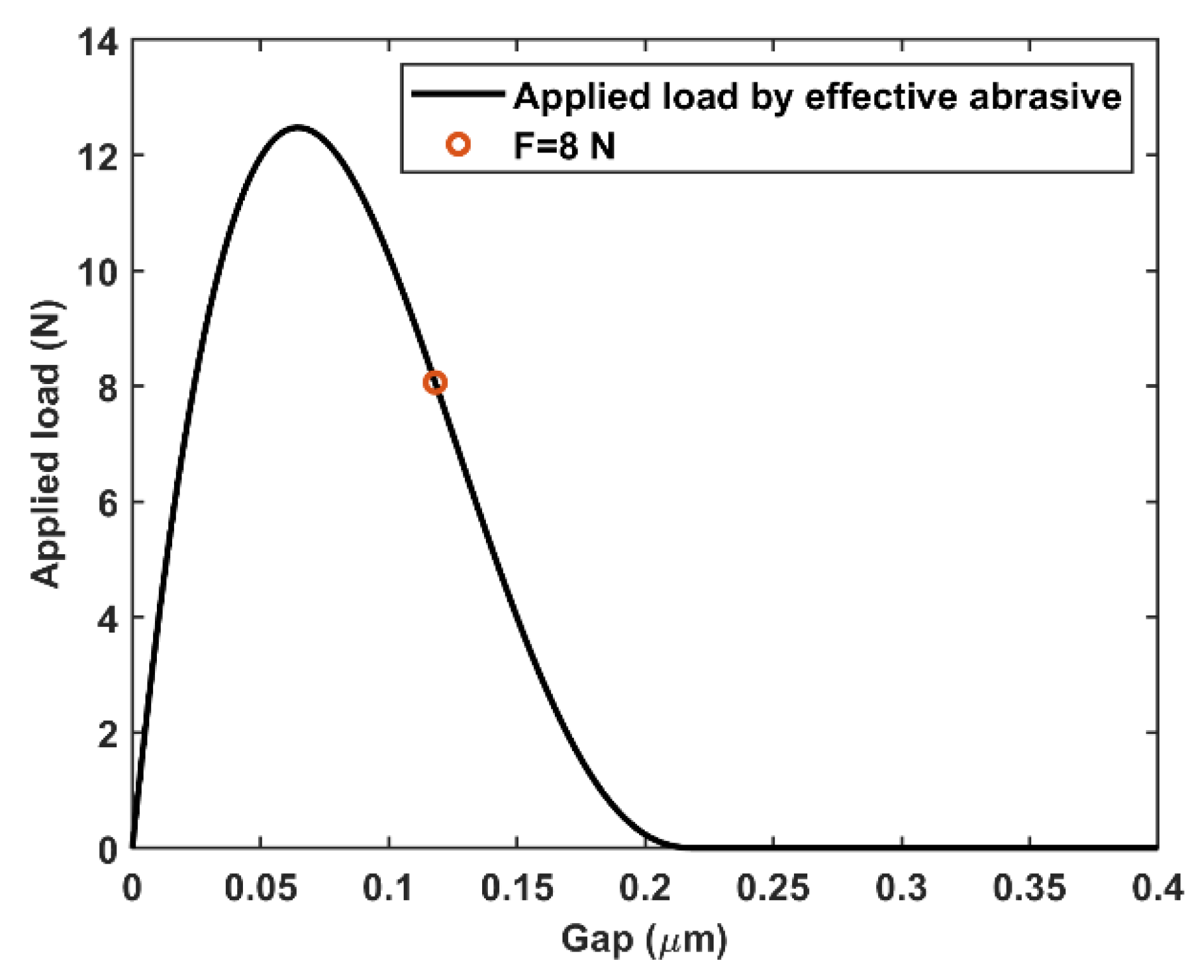
| νm | 0.26 | Em | 18.5 × 10¹⁰ Pa | Gap | 0.1185 μm |
|---|---|---|---|---|---|
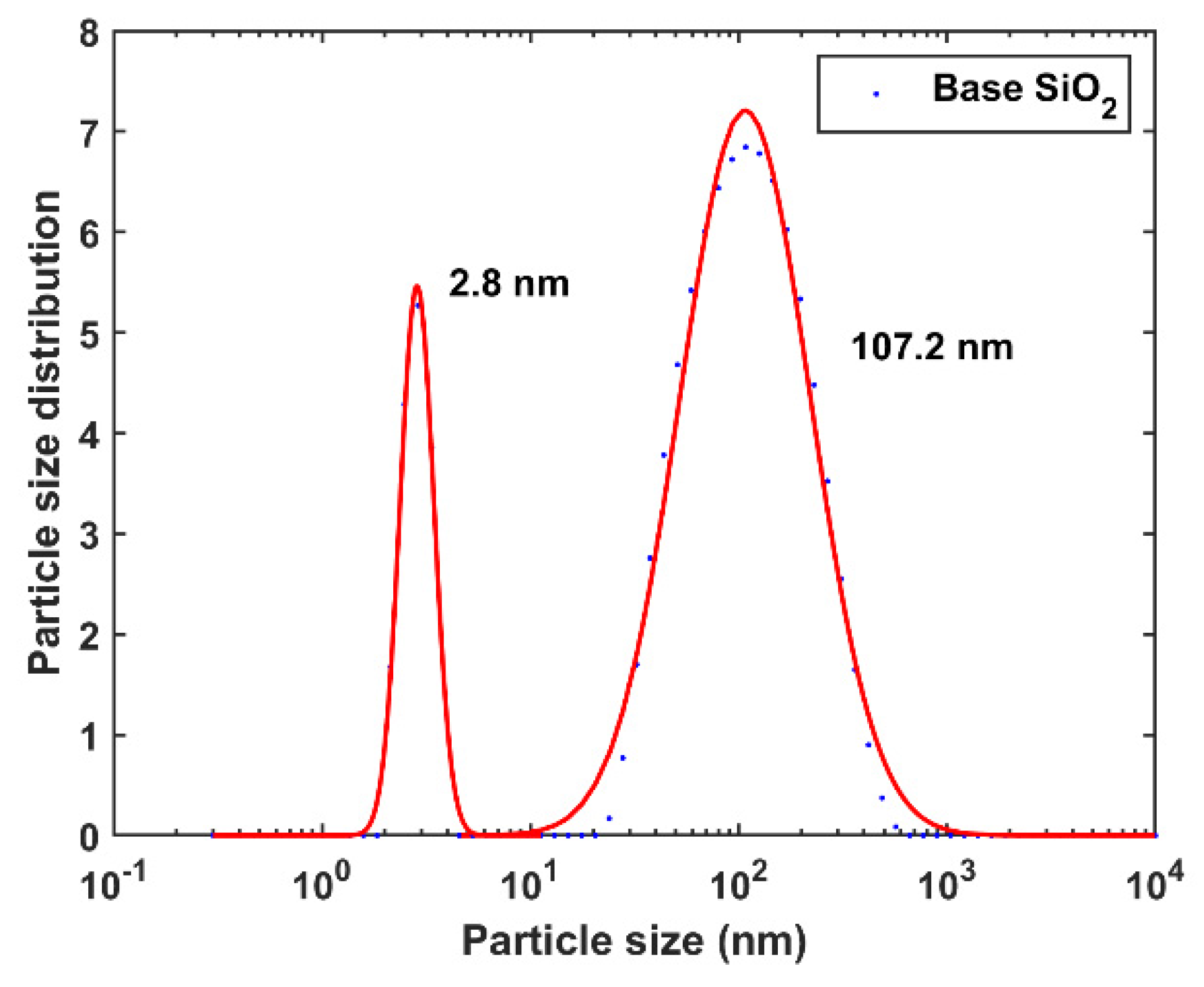
| νp | 0.17 | Ep | 7.20 × 10¹⁰ Pa | ASD peak 1 | 2.8 nm |
| νl | 0.22 | El | 3.14 × 10⁸ Pa | ASD peak 2 | 107.2 nm |
| Slurry concentration | 15 wt.% | Applied load | 8 N | ||
Publisher’s Note: MDPI stays neutral with regard to jurisdictional claims in published maps and institutional affiliations. |
© 2022 by the authors. Licensee MDPI, Basel, Switzerland. This article is an open access article distributed under the terms and conditions of the Creative Commons Attribution (CC BY) license (https://creativecommons.org/licenses/by/4.0/).
Share and Cite
Xia, J.; Yu, J.; Lu, S.; Huang, Q.; Xie, C.; Wang, Z. Surface Morphology Evolution during Chemical Mechanical Polishing Based on Microscale Material Removal Modeling for Monocrystalline Silicon. Materials 2022, 15, 5641. https://doi.org/10.3390/ma15165641
Xia J, Yu J, Lu S, Huang Q, Xie C, Wang Z. Surface Morphology Evolution during Chemical Mechanical Polishing Based on Microscale Material Removal Modeling for Monocrystalline Silicon. Materials. 2022; 15(16):5641. https://doi.org/10.3390/ma15165641
Chicago/Turabian StyleXia, Jingjing, Jun Yu, Siwen Lu, Qiushi Huang, Chun Xie, and Zhanshan Wang. 2022. "Surface Morphology Evolution during Chemical Mechanical Polishing Based on Microscale Material Removal Modeling for Monocrystalline Silicon" Materials 15, no. 16: 5641. https://doi.org/10.3390/ma15165641
APA StyleXia, J., Yu, J., Lu, S., Huang, Q., Xie, C., & Wang, Z. (2022). Surface Morphology Evolution during Chemical Mechanical Polishing Based on Microscale Material Removal Modeling for Monocrystalline Silicon. Materials, 15(16), 5641. https://doi.org/10.3390/ma15165641