
Influence of Mn, Fe, Co, and Cu Doping on the Photoelectric Properties of 1T HfS2 Crystals


Abstract
:1. Introduction
2. Materials and Methods
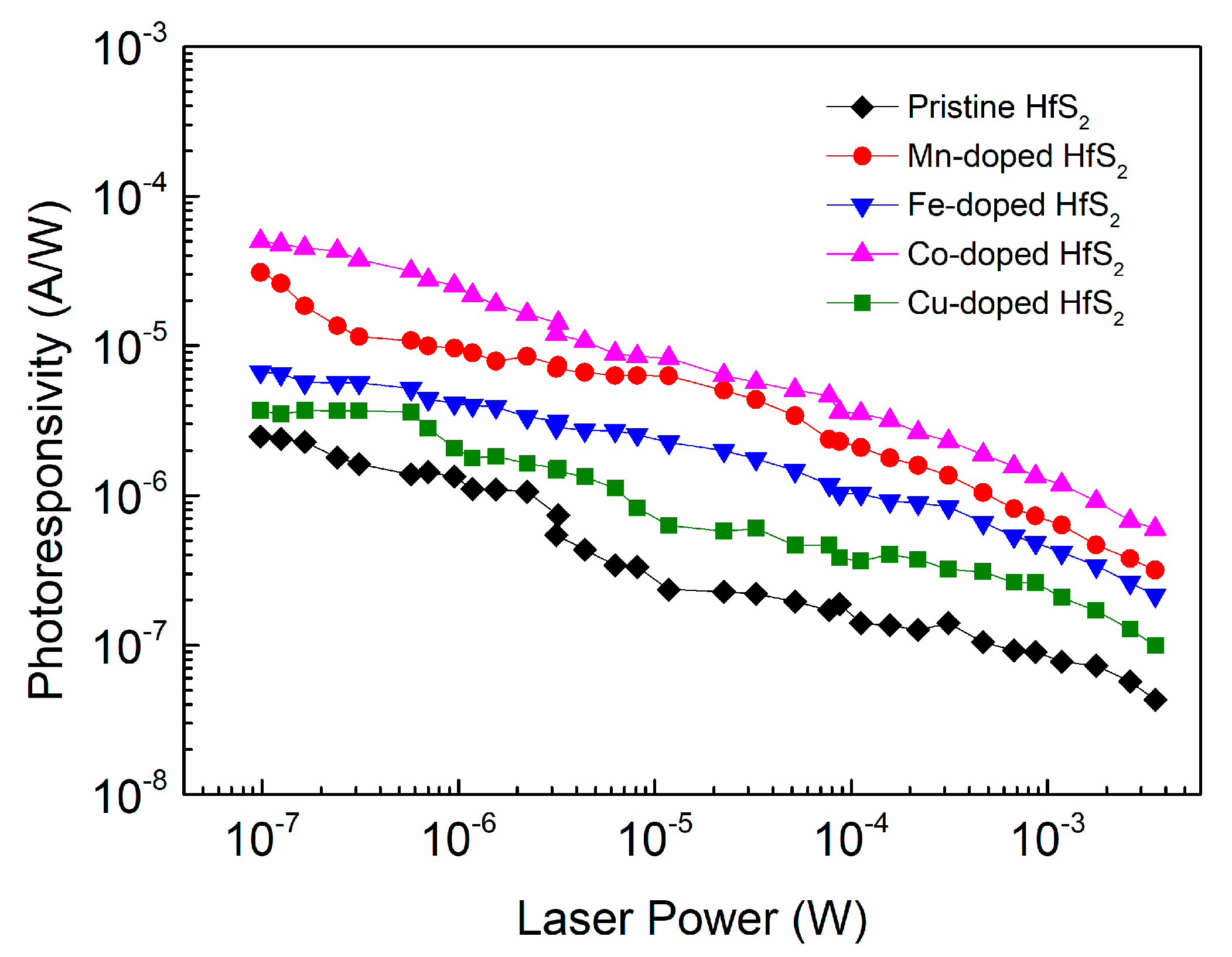
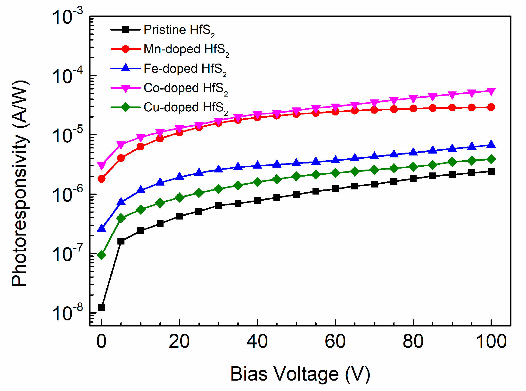
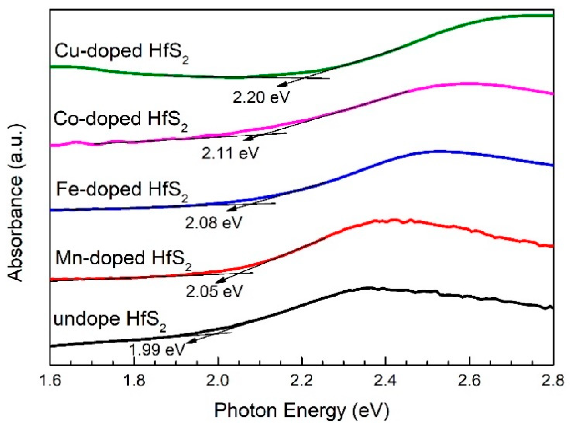
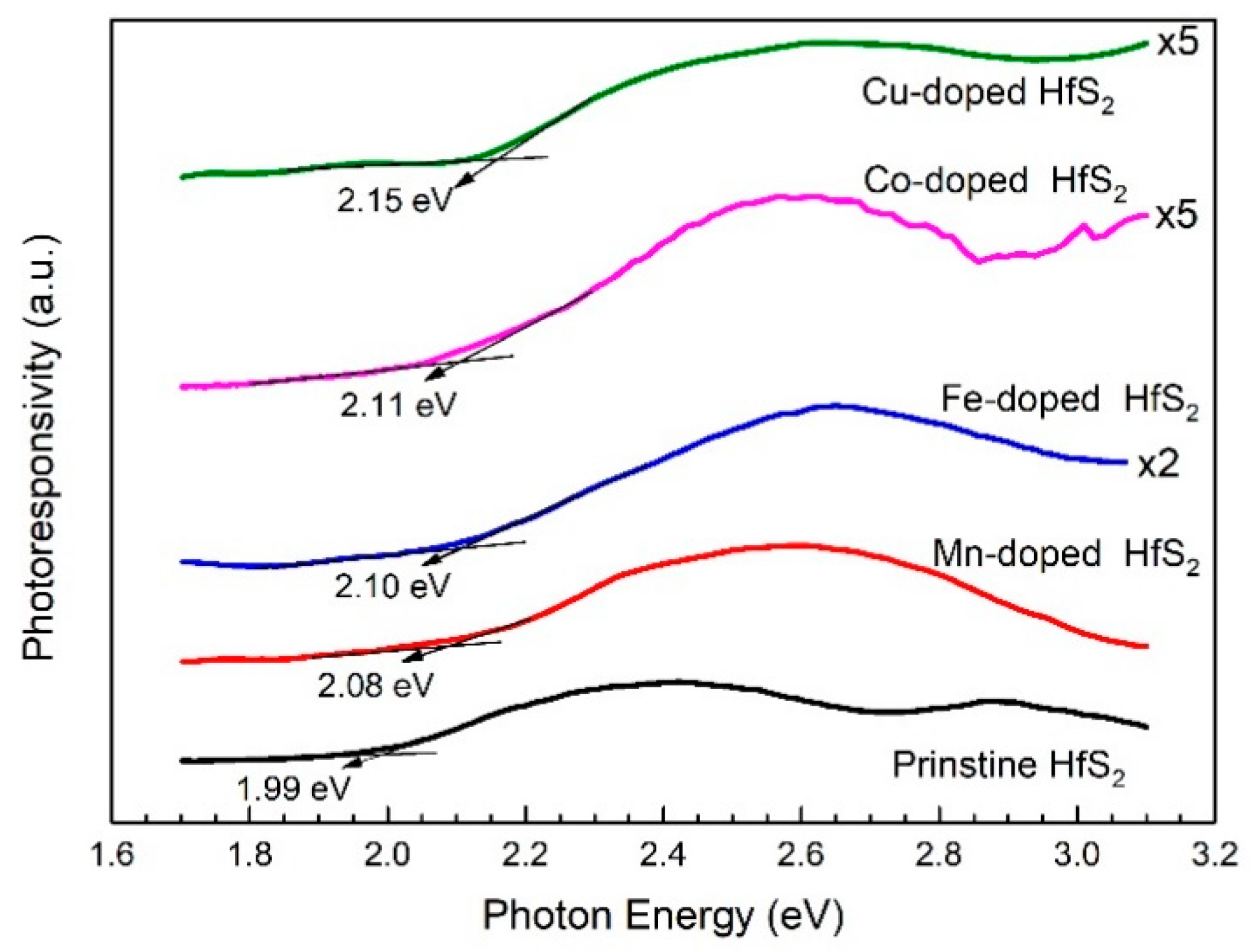
3. Results and Discussion
4. Conclusions
Author Contributions
Funding
Institutional Review Board Statement
Informed Consent Statement
Data Availability Statement
Conflicts of Interest
References
- Wilson, J.A.; Yoffe, A.D. The transition metal dichalcogenides discussion and interpretation of the observed optical, electrical and structural properties. Adv. Phys. 1969, 18, 193–335. [Google Scholar] [CrossRef]
- Friend, R.H.; Yoffe, A.D. Electronic properties of intercalation complexes of the transition metal dichalcogenides. Adv. Phys. 1987, 36, 1–94. [Google Scholar] [CrossRef]
- Zeng, H.; Cui, X. An optical spectroscopic study on two dimensional group-VI transition metal dichalcogenides. Chem. Soc. Rev. 2015, 44, 2629–2642. [Google Scholar] [CrossRef] [PubMed]
- Voiry, D.; Mohite, A.; Chhowalla, M. Phase engineering of transition metal dichalcogenides. Chem. Soc. Rev. 2015, 44, 2702–2712. [Google Scholar] [CrossRef]
- Kolobov, A.V.; Tominaga, J. Two-Dimensional Transition-Metal Dichalcogenides; Springer: Cham, Switzerland, 2016; pp. 29–77. [Google Scholar]
- Choi, W.; Choudhary, N.; Han, G.H.; Park, J.; Akinwande, D.; Lee, Y.H. Recent development of two-dimensional transition metal dichalcogenides and their applications. Mater. Today 2017, 20, 116–130. [Google Scholar] [CrossRef]
- Manzeli, S.; Ovchinnikov, D.; Pasquier, D.; Yazyev, O.V.; Kis, A. 2D transition metal dichalcogenides. Nat. Rev. Mater. 2017, 2, 17033. [Google Scholar] [CrossRef]
- Li, H.; Jia, X.; Zhang, Q.; Wang, X. Metallic Transition-Metal Dichalcogenide Nanocatalysts for Energy Conversion. Chem 2018, 4, 1510–1537. [Google Scholar] [CrossRef] [Green Version]
- Chhowalla, M.; Shin, H.S.; Eda, G.; Li, L.J.; Loh, K.P.; Zhang, H. The chemistry of two-dimensional layered transition metal dichalcogenide nanosheets. Nat. Chem. 2013, 5, 263–275. [Google Scholar] [CrossRef]
- Frindt, R.F. Single Crystals of MoS2 Several Molecular Layers Thick. J. Appl. Phys. 1966, 37, 1928–1929. [Google Scholar] [CrossRef]
- Joensen, P.; Frindt, R.F.; Morrison, S.R. Single-layer MoS2. Mat. Res. Bull. 1986, 21, 457–461. [Google Scholar] [CrossRef]
- Liu, Q.; Li, X.; He, Q.; Khalil, A.; Liu, D.; Xiang, T.; Wu, X.; Song, L. Gram-scale aqueous synthesis of stable few-layered 1T-MoS2: Applications for visible-light-driven photocatalytic hydrogen evolution. Small 2015, 11, 5556–5564. [Google Scholar] [CrossRef]
- Samadi, M.; Sarikhani, N.; Zirak, M.; Zhang, H.; Zhang, H.L.; Moshfegh, A.Z. Group 6 transition metal dichalcogenide nanomaterials: Synthesis, applications and future perspectives. Nanoscale Horiz. 2018, 3, 90–204. [Google Scholar] [CrossRef]
- Radisavljevic, B.; Radenovic, A.; Brivio, J.; Giacometti, V.; Kis, A. Single-layer MoS2 transistors. Nat. Nanotechnol. 2011, 6, 147–150. [Google Scholar] [CrossRef]
- Splendiani, A.; Sun, L.; Zhang, Y.; Li, T.; Kim, J.; Chim, C.Y.; Galli, G.; Wang, F. Emerging photoluminescence in monolayer MoS2. Nano Lett. 2010, 10, 1271–1275. [Google Scholar] [CrossRef]
- Mak, K.F.; Lee, C.; Hone, J.; Shan, J.; Heinz, T.F. Atomically thin MoS2: A new direct-gap semiconductor. Phys. Rev. Lett. 2010, 105, 136805. [Google Scholar] [CrossRef] [Green Version]
- Yan, C.; Gong, C.; Wangyang, P.; Chu, J.; Hu, K.; Li, C.; Wang, X.; Du, X.; Zhai, T.; Li, Y.; et al. 2D group IVB transition metal dichalcogenides. Adv. Funct. Mater. 2018, 28, 1803305. [Google Scholar] [CrossRef]
- Abdulsalam, M.; Joubert, D.P. Optical spectrum and excitons in bulk and monolayer MX2 (M = Zr, Hf; X = S, Se). Phys. Status Solidi B 2016, 253, 705–711. [Google Scholar] [CrossRef]
- Jiang, H. Structural and electronic properties of ZrX2 and HfX2 (X = S and Se) from first principles calculations. J. Chem. Phys. 2011, 134, 204705. [Google Scholar] [CrossRef] [PubMed]
- Greenway, D.L.; Nitsche, R. Preparation and optical properties of group IV-VI2 chalcogenides having the CdI2 structure. J. Phys. Chem. Solids 1965, 26, 1445–1458. [Google Scholar] [CrossRef]
- Roubi, L.; Garlone, G. Resonance Raman spectrum of HfS2 and ZrS2. Phys. Rev. B 1988, 37, 6808–6812. [Google Scholar] [CrossRef] [PubMed]
- Terashima, K.; Imai, I. Indirect absorption edge of ZrS2 and HfS2. Solid State Commun. 1987, 63, 315–318. [Google Scholar] [CrossRef]
- Gaiser, C.; Zandt, T.; Krapf, A.; Serverin, R.; Janowitz, C.; Manzke, R. Band-gap engineering with HfSxSe2−x. Phys. Rev. B 2004, 69, 075205. [Google Scholar] [CrossRef]
- Lee, P.A.; Said, G.; Davis, R.; Lim, T.H. On the optical properties of some layer compound. J. Phys. Chem. Solids 1969, 30, 2719–2729. [Google Scholar] [CrossRef]
- Moustafa, M.; Zandt, T.; Janowitz, C.; Manzke, R. Growth and band gap determination of the ZrSxSe2−x single crystal series. Phys. Rev. B 2009, 80, 035206. [Google Scholar] [CrossRef]
- Wang, D.; Zhang, X.; Wang, Z. Recent advances in properties, synthesis and applications of two-dimensional HfS2. J. Nanosci. Nanotechnol. 2018, 18, 7319–7334. [Google Scholar] [CrossRef]
- Kaur, H.; Yadav, S.; Srivastava, A.K.; Singh, N.; Rath, S.; Schneider, J.J.; Sinha, O.P.; Srivastava, R. High-yield synthesis and liquid-exfoliation of two-dimensional belt-like hafnium disulphide. Nano Res. 2018, 11, 343–353. [Google Scholar] [CrossRef] [Green Version]
- Wang, D.; Meng, J.; Zhang, X.; Guo, G.; Yin, Z.; Liu, H.; Cheng, L.; Gao, M.; You, J.; Wang, R. Selective direct growth of atomic layered HfS2 on hexagonal boron nitride for high performance photodetectors. Chem. Mater. 2018, 30, 3819–3826. [Google Scholar] [CrossRef]
- Li, N.; Wang, Y.; Sun, H.; Hu, J.; Zheng, M.; Ye, S.; Wang, Q.; Li, Y.; He, D.; Wang, J.; et al. Resistive switching behaviors and mechanisms of HfS2 film memory devices studied by experiments and density functional theory calculations. Appl. Phys. Lett. 2020, 116, 063503. [Google Scholar] [CrossRef]
- Yin, J.; Zhu, F.; Lai, J.; Chen, H.; Zhang, M.; Zhang, J.; Wang, J.; He, T.; Zhang, B.; Yuan, J.; et al. Hafnium sulfide nanosheets for ultrafast photonic device. Adv. Opt. Mater. 2018, 7, 1801303. [Google Scholar] [CrossRef]
- Hoat, D.M.; Ponce-Pérez, R.; Vu, T.V.; Rivas-Silva, J.F.; Cocoletzi, G.H. Theoretical analysis of the HfS2 monolayer electronic structure and optical properties under vertical strain effects. Optik 2021, 225, 165718. [Google Scholar] [CrossRef]
- Fu, L.; Wang, F.; Wu, B.; Wu, N.; Huang, W.; Wang, H.; Jin, C.; Zhuang, L.; He, J.; Fu, L.; et al. Van der Waals epitaxial growth of atomic layered HfS2 crystals for ultrasensitive near-infrared phototransistors. Adv. Mater. 2017, 29, 1700439. [Google Scholar] [CrossRef] [PubMed]
- Xu, K.; Huang, Y.; Chen, B.; Xia, Y.; Lei, W.; Wang, Z.; Wang, Q.; Wang, F.; Yin, L.; He, J. Toward high-performance top-gate ultrathin HfS2 field-effect transistors by interface engineering. Small 2016, 12, 3106–3111. [Google Scholar] [CrossRef]
- Xu, K.; Wang, Z.; Wang, F.; Huang, Y.; Wang, F.; Yin, L.; Jiang, C.; He, J. Ultrasensitive phototransistors based on few-layered HfS2. Adv. Mater. 2015, 27, 7881–7887. [Google Scholar] [CrossRef]
- Kanazawa, T.; Amemiya, T.; Ishikawa, A.; Upadhyaya, V.; Tsuruta, K.; Tanaka, T.; Miyamoto, Y. Few-layer HfS2 transistors. Sci. Rep. 2016, 6, 22277. [Google Scholar] [CrossRef] [PubMed]
- Mattinen, M.; Popov, G.; Vehkamäki, M.; King, P.J.; Mizohata, K.; Jalkanen, P.; Räisänen, J.; Leskelä, M.; Ritala, M. Atomic layer deposition of emerging 2D semiconductors, HfS2 and ZrS2, for optoelectronics. Chem. Mater. 2019, 31, 5713–5724. [Google Scholar] [CrossRef] [Green Version]
- Zhang, W.; Huang, Z.; Zhang, W.; Li, Y. Two-dimensional semiconductors with possible high room temperature mobility. Nano Res. 2014, 7, 1731–1737. [Google Scholar] [CrossRef] [Green Version]
- Suh, J.; Park, T.E.; Lin, D.Y.; Fu, D.; Park, J.; Jung, H.J.; Chen, Y.; Ko, C.; Jang, C.; Sun, Y.; et al. Doping against the native propensity of MoS2: Degenerate hole doping by cation substitution. Nano Lett. 2014, 14, 6976–6982. [Google Scholar] [CrossRef] [PubMed]
- Zhang, K.; Feng, S.; Wang, J.; Azcatl, A.; Lu, N.; Addou, R.; Wang, N.; Zhou, C.; Lerach, J.O.; Bojan, V.; et al. Manganese doping of monolayer MoS2: The substrate is critical. Nano Lett. 2015, 15, 6586–6591. [Google Scholar] [CrossRef]
- Gong, Y.; Liu, Z.; Lupini, A.; Shi, G.; Lin, J.; Najmaei, S.; Lin, Z.; Elias, A.L.; Berkdemir, A.; You, G.; et al. Band gap engineering and layer-by-layer mapping of selenium-doped molybdenum disulfide. Nano Lett. 2014, 14, 442–449. [Google Scholar] [CrossRef]
- Mouri, S.; Miyauchi, Y.; Matsuda, K. Tunable photoluminescence of monolayer MoS2 via chemical doping. Nano Lett. 2013, 13, 5944–5948. [Google Scholar] [CrossRef] [Green Version]
- Li, B.; Xing, T.; Zhong, M.; Huang, L.; Lei, N.; Zhang, J.; Li, J.; Wei, Z. A two-dimensional Fe-doped SnS2 magnetic semiconductor. Nat. Commun. 2017, 8, 1958. [Google Scholar] [CrossRef]
- Zhao, X.; Xia, C.; Wang, T.; Dai, X.; Yang, L. Characteristics of n- and p-type dopants in 1T-HfS2 monolayer. J. Alloy. Compd. 2016, 689, 302–306. [Google Scholar] [CrossRef]
- Lu, H.; Guo, Y.; Robertson, J. Band edge states, intrinsic defects, and dopants in monolayer HfS2 and SnS2. Appl. Phys. Lett. 2018, 112, 062105. [Google Scholar] [CrossRef] [Green Version]
- Singh, D.; Ahuja, R. Enhanced optoelectronic and thermoelectric properties by intrinsic structural defects in monolayer HfS2. ACS Appl. Energy Mater. 2019, 2, 6891–6903. [Google Scholar] [CrossRef]
- Zhao, X.; Wang, T.; Wang, G.; Dai, X.; Xia, C.; Yang, L. Electronic and magnetic properties of 1T-HfS2 by doping transition-metal atoms. Appl. Surf. Sci. 2016, 383, 151–158. [Google Scholar] [CrossRef]
- Ma, X.; Zhao, X.; Wu, N.; Xin, Q.; Liu, X.; Wang, T.; Wei, S. Ferromagnetic properties of Mn-doped HfS2 monolayer under strain. Solid State Commun. 2017, 268, 15–19. [Google Scholar] [CrossRef]
- Zhao, X.; Liu, X.; Wang, T.; Wei, S. Effect of structural defects on electronic and magnetic properties in pristine and Cr-doped HfS2 monolayer. J. Alloy. Compd. 2018, 731, 303–309. [Google Scholar] [CrossRef]
- Ali, A.; Zhang, J.M.; Muhammad, I.; Wei, X.M.; Ahmad, I.; Rehman, M.U. Changing the electronic and magnetic properties of monolayer HfS2 by doping and vacancy defects: Insight from first-principles calculations. Phys. Status Solidi B 2020, 257, 1900768. [Google Scholar] [CrossRef]
- Obodo, K.O.; Gebreyesus, G.; Ouma, C.N.M.; Obodo, J.T.; Ezeonu, S.O.; Rai, D.P.; Bouhafs, B. Controlling the electronic and optical properties of HfS2 monolayers via lanthanide substitutional doping: A DFT+U study. RSC Adv. 2020, 10, 15670. [Google Scholar] [CrossRef] [Green Version]
- Lucovsky, G.; White, R.M.; Benda, J.A.; Revelli, J.F. Infrared-reflectance spectra of layered group-IV and group-VI transition-metal dichalcogenides. Phys. Rev. B 1973, 7, 3859–3870. [Google Scholar] [CrossRef]
- Traving, M.; Seydel, T.; Kipp, L.; Skibowski, M.; Starrost, F.; Krasovskii, E.E.; Perlov, A.; Schattke, W. Combined photoemission and inverse photoemission study of HfS2. Phys. Rev. B 2001, 63, 035107. [Google Scholar] [CrossRef] [Green Version]
- Neal, S.N.; Li, S.; Birol, T.; Musfeldt, J.L. Chemical bonding and Born charge in 1T-HfS2. NPJ 2D Mater. Appl. 2021, 5, 45. [Google Scholar] [CrossRef]
- Iwasaki, T.; Kuroda, N.; Nishina. Y. Anisotropy of lattice dynamical properties in ZrS2 and HfS2. J. Phys. Soc. Jpn. 1982, 51, 2233–2240. [Google Scholar] [CrossRef]
- Uchida, S.; Tanaka, S. Optical phonon modes and localized effective charges of transition-metal dichalcogenides. J. Phys. Soc. Jpn. 1978, 45, 153–161. [Google Scholar] [CrossRef]
- Chen, J. Phonons in bulk and monolayer HfS2 and possibility of phonon-mediated superconductivity: A first-principles study. Solid State Commun. 2016, 237–238, 14–18. [Google Scholar] [CrossRef]
- Cingolani, A.; Lugara, M.; Scamarcio, G.; Levy, F. The Raman scattering in hafnium disulfide. Solid State Comm. 1987, 62, 121–123. [Google Scholar] [CrossRef]
- Cingolani, A.; Lugara, M.; Levy, F. Resonance Raman scattering in HfSe, and HfS. Phys. Scripta 1988, 37, 389–391. [Google Scholar] [CrossRef]
- Zheng, B.; Chen, Y.; Wang, Z.; Qi, F.; Huang, Z.; Hao, X.; Li, P.; Zhang, W.; Li, Y. Vertically oriented few-layered HfS2 nanosheets: Growth mechanism and optical properties. 2D Mater. 2016, 3, 035024. [Google Scholar] [CrossRef]
- Ibáñez, J.; Woźniak, T.; Dybala, F.; Oliva, R.; Hernández, S.; Kudrawiec, R. High-pressure Raman scattering in bulk HfS2: Comparison of density functional theory methods in layered MS2 compounds (M = Hf, Mo) under compression. Sci. Rep. 2018, 8, 12757. [Google Scholar] [CrossRef] [PubMed]
- Lin, Y.F.; Jian, W.B.; Wang, C.P.; Suen, Y.W.; Wu, Z.Y.; Chen, F.R.; Kai, J.J.; Lin, J.J. Contact to ZnO and intrinsic resistances of individual ZnO nanowires with a circular cross section. Appl. Phys. Lett. 2007, 90, 223117. [Google Scholar] [CrossRef] [Green Version]
- Lin, T.T.; Young, S.L.; Kung, C.Y.; Chen, H.Z.; Kao, M.C.; Chang, M.C.; Ou, C.R. Variable-range hopping and thermal activation conduction of Y-doped ZnO nanocrystalline films. IEEE Trans. Nanotechnol. 2014, 13, 425–430. [Google Scholar] [CrossRef] [Green Version]
- Pleshchev, V.G.; Selezneva, N.V. Electrical and magnetic properties of hafnium disulfide intercalated with iron atoms. Phys. Solid State 2018, 60, 250–255. [Google Scholar] [CrossRef]


| Sample | Hf (at. %) | S (at. %) | Dopant (at. %) |
|---|---|---|---|
| Pristine HfS2 | 34.26 | 65.75 | |
| Mn-doped HfS2 | 31.44 | 68.00 | 0.54 |
| Fe-doped HfS2 | 37.92 | 61.91 | 0.16 |
| Co-doped HfS2 | 32.30 | 67.09 | 0.60 |
| Cu-doped HfS2 | 30.78 | 68.24 | 0.96 |
| Sample | d100 (Å) | d110 (Å) | a (Å) | c (Å) |
|---|---|---|---|---|
| 1T HfS2 | 3.63 1 | 5.85 1 | ||
| Pristine HfS2 | 3.17 | 1.84 | 3.66 | 5.85 |
| Mn-doped HfS2 | 3.09 | 1.79 | 3.57 | 5.86 |
| Fe-doped HfS2 | 2.98 | 1.71 | 3.44 | 5.86 |
| Co-doped HfS2 | 2.92 | 1.66 | 3.37 | 5.87 |
| Cu-doped HfS2 | 2.82 | 1.59 | 3.26 | 5.87 |
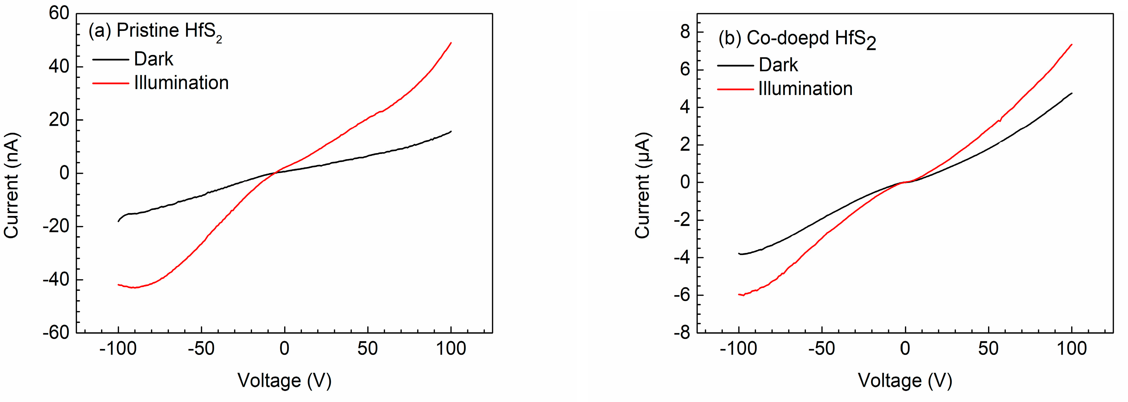
| Sample | ρ (Ω⋅m) | |
|---|---|---|
| Dark | Illumination | |
| Pristine HfS2 | 2.184 × 10⁶ | 7.231 × 10⁵ |
| Mn-doped HfS2 | 2.847 × 10⁵ | 1.791 × 10⁵ |
| Fe-doped HfS2 | 4.211 × 10⁵ | 1.976 × 10⁵ |
| Co-doped HfS2 | 8.898 × 10³ | 5.545 × 10³ |
| Cu-doped HfS2 | 1.917 × 10⁶ | 1.389 × 10⁶ |
| Frequency (Hz) | ||||||||
|---|---|---|---|---|---|---|---|---|
| 1 | 100 | 500 | 1000 | |||||
| Sample | trise (ms) | tfall (ms) | trise (ms) | tfall (ms) | trise (μs) | tfall (μs) | trise (μs) | tfall (μs) |
| Pristine HfS2 | 13.20 | 17.44 | 0.28 | 0.66 | 175 | 264 | 123 | 132 |
| Mn-doped HfS2 | 8.26 | 10.09 | 0.26 | 0.32 | 49 | 145 | 44 | 85 |
| Fe-doped HfS2 | 8.71 | 11.46 | 0.29 | 0.38 | 53 | 157 | 48 | 93 |
| Co-doped HfS2 | 7.84 | 9.41 | 0.24 | 0.29 | 43 | 121 | 40 | 62 |
| Cu-doped HfS2 | 9.37 | 14.3 | 0.27 | 0.53 | 62 | 187 | 72 | 129 |
| Frequency (Hz) | ||||
|---|---|---|---|---|
| 1 | 100 | 500 | 1000 | |
| Sample | Current Amplitude (nA) | |||
| Pristine HfS2 | 4.73 | 3.06 | 2.21 | 1.17 |
| Mn-doped HfS2 | 818 | 712 | 630 | 450 |
| Fe-doped HfS2 | 428 | 308 | 206 | 212 |
| Co-doped HfS2 | 995 | 959 | 735 | 565 |
| Cu-doped HfS2 | 97.2 | 68.1 | 50.0 | 46.6 |
Publisher’s Note: MDPI stays neutral with regard to jurisdictional claims in published maps and institutional affiliations. |
© 2021 by the authors. Licensee MDPI, Basel, Switzerland. This article is an open access article distributed under the terms and conditions of the Creative Commons Attribution (CC BY) license (https://creativecommons.org/licenses/by/4.0/).
Share and Cite
Lin, D.-Y.; Shih, Y.-T.; Tseng, W.-C.; Lin, C.-F.; Chen, H.-Z. Influence of Mn, Fe, Co, and Cu Doping on the Photoelectric Properties of 1T HfS2 Crystals. Materials 2022, 15, 173. https://doi.org/10.3390/ma15010173
Lin D-Y, Shih Y-T, Tseng W-C, Lin C-F, Chen H-Z. Influence of Mn, Fe, Co, and Cu Doping on the Photoelectric Properties of 1T HfS2 Crystals. Materials. 2022; 15(1):173. https://doi.org/10.3390/ma15010173
Chicago/Turabian StyleLin, Der-Yuh, Yu-Tai Shih, Wei-Chan Tseng, Chia-Feng Lin, and Hone-Zern Chen. 2022. "Influence of Mn, Fe, Co, and Cu Doping on the Photoelectric Properties of 1T HfS2 Crystals" Materials 15, no. 1: 173. https://doi.org/10.3390/ma15010173
APA StyleLin, D.-Y., Shih, Y.-T., Tseng, W.-C., Lin, C.-F., & Chen, H.-Z. (2022). Influence of Mn, Fe, Co, and Cu Doping on the Photoelectric Properties of 1T HfS2 Crystals. Materials, 15(1), 173. https://doi.org/10.3390/ma15010173