
Inverted-Type InAlAs/InAs High-Electron-Mobility Transistor with Liquid Phase Oxidized InAlAs as Gate Insulator


Abstract
1. Introduction
2. Experimental
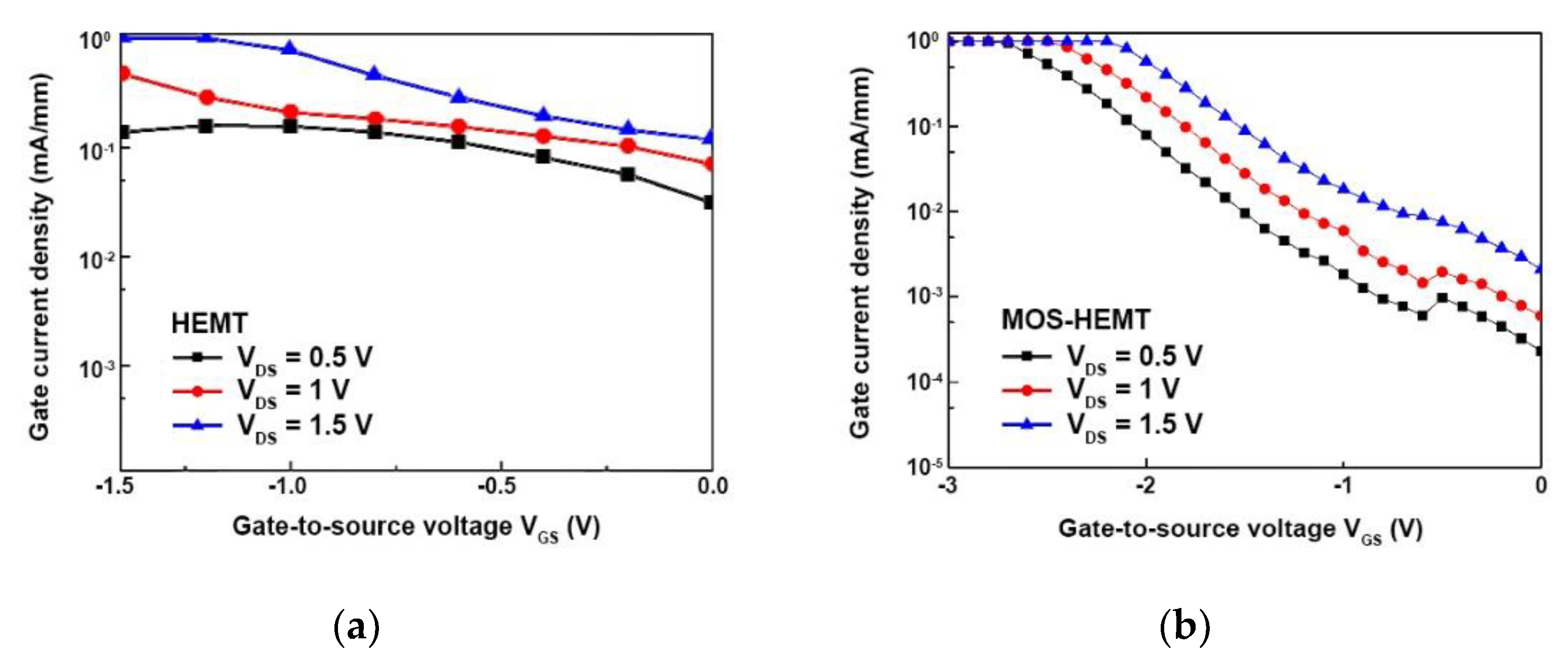
3. Results and Discussion
4. Conclusions
Author Contributions
Funding
Institutional Review Board Statement
Informed Consent Statement
Acknowledgments
Conflicts of Interest
References
- Del Alamo, J.A. Nanometre-scale electronics with III–V compound semiconductors. Nature 2011, 479, 317–323. [Google Scholar] [CrossRef] [PubMed]
- Smith, P.M.; Liu, S.M.J.; Kao, M.Y.; Ho, P.; Wang, S.C.; Duh, K.H.G.; Fu, S.T.; Chao, P.C. W-band high efficiency InP-based power HEMT with 600 GHz fmax. IEEE Microw. Guided Wave Lett. 1995, 5, 230–232. [Google Scholar] [CrossRef]
- Jo, H.B.; Baek, J.M.; Yun, D.Y.; Son, S.W.; Lee, J.H.; Kim, T.W.; Kim, D.H.; Tsutsumi, T.; Sugiyama, H.; Matsuzaki, H. Lg = 87 nm InAlAs/InGaAs high-electron-mobility transistors with a gm_max of 3 S/mm and fT of 559 GHz. IEEE Electron Device Lett. 2018, 39, 1640–1643. [Google Scholar] [CrossRef]
- Ng, G.I.; Pavlidis, D.; Quillec, M.; Chan, Y.J.; Jaffe, M.D.; Singh, J. Study of the consequence of excess indium in the active channel of InGaAs/InAlAs high electron mobility transistors on device properties. Appl. Phys. Lett. 1988, 52, 728–730. [Google Scholar] [CrossRef][Green Version]
- Matsumura, K.; Inoue, D.; NaKano, H.; Sawada, M.; Harada, Y.; Nakakado, T. A new high electron mobility transistor (HEMT) structure with a narrow quantum well formed by inserting a few monolayers in the channel. Jpn. J. Appl. Phys. 2018, 30, L166–L169. [Google Scholar] [CrossRef]
- Eugster, C.C.; Broekaert, T.P.E.; Del Alamo, J.A.; Fonstad, C.G. An InAlAs/InAs MODFET. IEEE Electron Device Lett. 1991, 12, 707–709. [Google Scholar] [CrossRef]
- Ko, H.; Takei, K.; Kapadia, R.; Chuang, S.; Fang, H.; Leu, P.W.; Ganapathi, K.; Plis, E.; Kim, H.S.; Chen, S.-Y.; et al. Ultrathin compound semiconductor on insulator layers for high-performance nanoscale transistors. Nature 2010, 468, 286–289. [Google Scholar] [CrossRef] [PubMed]
- Kim, K.-H.; Um, D.-S.; Lee, H.; Lim, S.; Chang, J.; Koo, H.C.; Oh, M.-W.; Ko, H.; Kim, H.-J. Gate-controlled spin-orbit interaction in InAs high-electron mobility transistor layers epitaxially transferred onto Si substrates. ACS Nano 2013, 7, 9106–9114. [Google Scholar] [CrossRef] [PubMed]
- Yamada, H.T.; Shigemasa, R.; Fujishiro, H.I.; Nishi, S.; Saito, T. Fabrication of 0.2 μm gate pseudomorphic inverted HEMT by phase-shifting technology. Solid-State Electron. 1995, 38, 1631–1634. [Google Scholar] [CrossRef]
- Akazaki, T.; Takayanagi, H.; Enoki, T. Kink effect in an InAs inserted-channel InAlAs/InGaAs inverted HEMT at low temperature. IEEE Electron Device Lett. 1996, 17, 378–380. [Google Scholar] [CrossRef]
- Li, Q.; Zhou, X.; Tang, C.W.; Lau, K.M. High-performance inverted In0.53Ga0.47As MOSHEMTs on a GaAs substrate with regrown source/drain by MOCVD. IEEE Electron Device Lett. 2012, 33, 1246–1248. [Google Scholar] [CrossRef]
- Minden, H.T. Thermal oxidation of GaAs. J. Electrochem. Soc. 1962, 109, 733. [Google Scholar] [CrossRef]
- Coleman, D.J.; Shaw, D.W.; Dobrott, R.D. On the mechanism of GaAs anodization. J. Electrochem. Soc. 1977, 124, 239–241. [Google Scholar] [CrossRef]
- Bertrand, P.A. The photochemical oxidation of GaAs. Photochem. Oxid. Gaas. 1985, 132, 973–976. [Google Scholar] [CrossRef]
- Ren, F.; Kuo, J.M.; Hong, M.; Hobson, W.S.; Lothian, J.R.; Lin, J.; Tsai, H.S.; Mannaerts, J.P.; Kwo, J.; Chu, S.N.G.; et al. Ga2O3(Gd2O3)/InGaAs enhancement-mode n-channel MOSFETs. IEEE Electron Device Lett. 1998, 19, 309–311. [Google Scholar] [CrossRef]
- Ye, P.; Wilk, G.; Kwo, J.; Yang, B.; Gossmann, H.-J.; Frei, M.; Chu, S.; Mannaerts, J.; Sergent, M.; Hong, M.; et al. GaAs MOSFET with oxide gate dielectric grown by atomic layer deposition. IEEE Electron Device Lett. 2003, 24, 209–211. [Google Scholar] [CrossRef]
- Paul, N.C.; Nakamura, K.; Seto, H.; Iiyama, K.; Takamiya, S. Oxidation of InAlAs and its application to gate in-sulator of InAlAs/InGaAs metal oxide semiconductor high electron mobility transistor. Jpn. J. Appl. Phys. 2005, 44, 1174–1180. [Google Scholar] [CrossRef]
- Bae, S.J.; Kim, J.M.; Park, C.Y.; Lee, Y.T. Characteristics of InAlAs/InP and InAlP/GaAs native oxides. Solid-State Electron. 2006, 50, 1625–1628. [Google Scholar] [CrossRef]
- Wang, H.-H.; Huang, C.-J.; Wang, Y.-H.; Houng, M.-P. Liquid phase chemical-enhanced oxidation for GaAs operated near room temperature. Jpn. J. Appl. Phys. 1998, 37, L67–L70. [Google Scholar] [CrossRef]
- Lee, K.-W.; Lee, K.-L.; Lin, X.-Z.; Tu, C.-H.; Wang, Y.-H. Improvement of impact ionization effect and subthreshold current in InAlAs/InGaAs metal–oxide–semiconductor metamorphic HEMT with a liquid-phase oxidized InAlAs as gate insulator. IEEE Trans. Electron Devices 2007, 54, 418–424. [Google Scholar] [CrossRef]
- Lee, K.-W.; Lin, K.-L.; Lin, H.-C.; Tu, C.-H.; Hu, C.-C.; Wang, Y.-H. Near-room-temperature selective oxidation on InAlAs and application to In0.52Al0.48As/In0.53Ga0.47As metamorphic HEMTs. J. Electrochem. Soc. 2007, 154, H957–H961. [Google Scholar] [CrossRef]
- Lee, K.-W.; Lin, H.-C.; Lee, K.-L.; Hsieh, C.-H.; Wang, Y.-H. Comprehensive study of InAlAs/InGaAs metamorphic high electron mobility transistor with oxidized InAlAs gate. J. Electrochem. Soc. 2009, 156, H925–H929. [Google Scholar] [CrossRef]
- Hill, R.J.W.; Droopad, R.; Moran, D.A.J.; Li, X.; Zhou, H.; Macintyre, D.; Thoms, S.; Ignatova, O.; Asenov, A.; Ra-jagopalan, K.; et al. 1 μm gate length, In0.75Ga0.25As channel, thin body n-MOSFET on InP substrate with transconductance of 737 μS/μm. Electron. Lett. 2008, 44, 498–500. [Google Scholar] [CrossRef]
- Duh, K.; Chao, P.-C.; Smith, P.; Lester, L.; Lee, B.; Ballingall, J.; Kao, M.-Y. High-performance Ka-band and V-band HEMT low-noise amplifiers. IEEE Trans. Microw. Theory Tech. 1988, 36, 1598–1603. [Google Scholar] [CrossRef]
- Hamaizia, Z.; Sengouga, N.; Missous, M.; Yagoub, M. A 0.4dB noise figure wideband low-noise amplifier using a novel InGaAs/InAlAs/InP device. Mater. Sci. Semicond. Process. 2011, 14, 89–93. [Google Scholar] [CrossRef]
- Fukui, H. Optimal noise figure of microwave GaAs MESFET’s. IEEE Trans. Electron Devices 1979, 26, 1032–1037. [Google Scholar] [CrossRef]
- Hartnagel, H.L.; Katilius, R.; Matulionis, A. Microwave Noise in Semiconductor Devices; John Wiley & Sons, Inc.: Hoboken, NJ, USA, 2001. [Google Scholar]
- Huang, H.-K.; Wang, C.-S.; Chang, C.-P.; Wang, Y.-H.; Wu, C.-L.; Chang, C.-S. Noise characteristics of InGaP-gated PHEMTs under high current and thermal accelerated stresses. IEEE Trans. Electron Devices 2005, 52, 1706–1712. [Google Scholar] [CrossRef]
- Marsh, P.; Pavlidis, D.; Hong, K. InGaAs-Schottky contacts made by in situ plated and evaporated Pt—an analysis based on DC and noise characteristics. IEEE Trans. Electron Devices 1998, 45, 349–360. [Google Scholar] [CrossRef]


| Gate Oxide | With | Without |
|---|---|---|
| Maximum IDS (mA/mm) at VDS = 1.5 V | 509 | 441 |
| Peak gm (mS/mm) at VDS = 1.5 V | 327 | 243 |
| Turn-on voltage (V) | 3.98 | 1.54 |
| Reverse gate-to-drain breakdown voltage (V) | −4.6 | −2.5 |
| Minimum noise figure NFmin at 1.2 GHz (dB) | 5.88 | 9.44 |
| Associated gain at 1.2 GHz (dB) | 15.67 | 9.74 |
| Type | Inverted-Type (This Work) | Normal-Type Ref. [20] | Normal-Type Ref. [22] |
|---|---|---|---|
| Substrate | InP | GaAs | GaAs |
| Channel | In0.53Ga0.47As/ InAs/In0.53Ga0.47As | In0.53Ga0.47As | In0.53Ga0.47As |
| Hall mobility (cm2/Vs)/sheet carrier concentration (cm−2) @ 300 K | 14,262/2.07 × 1012 | 7000/2 × 1012 | 7000/2 × 1012 |
| Gate length (μm) | 1 | 0.65 | 0.65 |
| 0.65 | |||
| Maximum IDS (mA/mm) | 509 | 252 | 424 |
| Peak gm (mS/mm) | 327 | 226 | 254 |
Publisher’s Note: MDPI stays neutral with regard to jurisdictional claims in published maps and institutional affiliations. |
© 2021 by the authors. Licensee MDPI, Basel, Switzerland. This article is an open access article distributed under the terms and conditions of the Creative Commons Attribution (CC BY) license (http://creativecommons.org/licenses/by/4.0/).
Share and Cite
Chen, Y.-M.; Lin, H.-C.; Lee, K.-W.; Wang, Y.-H. Inverted-Type InAlAs/InAs High-Electron-Mobility Transistor with Liquid Phase Oxidized InAlAs as Gate Insulator. Materials 2021, 14, 970. https://doi.org/10.3390/ma14040970
Chen Y-M, Lin H-C, Lee K-W, Wang Y-H. Inverted-Type InAlAs/InAs High-Electron-Mobility Transistor with Liquid Phase Oxidized InAlAs as Gate Insulator. Materials. 2021; 14(4):970. https://doi.org/10.3390/ma14040970
Chicago/Turabian StyleChen, Yuan-Ming, Hsien-Cheng Lin, Kuan-Wei Lee, and Yeong-Her Wang. 2021. "Inverted-Type InAlAs/InAs High-Electron-Mobility Transistor with Liquid Phase Oxidized InAlAs as Gate Insulator" Materials 14, no. 4: 970. https://doi.org/10.3390/ma14040970
APA StyleChen, Y.-M., Lin, H.-C., Lee, K.-W., & Wang, Y.-H. (2021). Inverted-Type InAlAs/InAs High-Electron-Mobility Transistor with Liquid Phase Oxidized InAlAs as Gate Insulator. Materials, 14(4), 970. https://doi.org/10.3390/ma14040970