Article

Resistance Switching Effect of Memory Device Based on All-Inorganic Cspbbri2 Perovskite

1
Science and Technology on Electro-Optical Information Security Control Laboratory, Tianjin 300308, China
2
School of Physics, Beihang University, Beijing 100191, China
*
Author to whom correspondence should be addressed.
Materials 2021, 14(21), 6629; https://doi.org/10.3390/ma14216629
Submission received: 28 September 2021 / Revised: 23 October 2021 / Accepted: 28 October 2021 / Published: 3 November 2021
(This article belongs to the Special Issue State-of-the-Art Materials Science in China)

Abstract

:
In this study, the CsPbBrI2 perovskite film was prepared by the preparation of the sol-gel and the spin-coating method, and the cubic lattice was stabilized by introducing Br+ into the CsPbI3 film, which solved the problem of instability of the traditional perovskite phase. Based on the CsPbBrI2 perovskite film, the Ag/CsPbBrI2/ITO memory device with a resistance switching effect was prepared. The morphology and phase compositions of the film were analyzed by scanning electron microscope and X-ray diffraction. The non-volatile and repeatable resistance switching effect of the Ag/CsPbBrI2/ITO memory device was measured under open-air conditions. The experimental results show that the surface of the CsPbBrI2 perovskite film is uniform and dense, and the Ag/CsPbBrI2/ITO memory device has an order of magnitude resistance-on-off ratio after 500 cycles of cyclic voltage. This study shows that Ag/CsPbBrI2/ITO memory devices based on CsPbBrI2 perovskite films have potential applications in the field of non-volatile memory devices. At the same time, the transient properties of the CsPbBrI2 film that can quickly dissolve in deionized water make it potentially useful in short-period data storage units and implantable electronic devices with human or environmental sensors.

1. Introduction

Due to the rapid development of semiconductor technology, transient electronic memory devices have reached their limits of scale. The research of new memory devices is very urgent for the high cost and power limitations of the current transient memory devices. There are four existing memory types, such as Ferroelectric Random-Access Memory (FeRAM), Magnetoresistive Random-Access Memory (MRAM), Phase Change Random-Access Memory (PRAM), Resistance Random-Access Memory (ReRAM) and charge trapping memory devices of two-dimensional materials. Resistive random-access memory is a new type of random-access memory device based on the resistance switching effect. It has outstanding superiority compared with traditional random-access memory due to its scalability, low power consumption, fast switching speed, durability and long data retention characteristics [1,2,3,4,5,6]. Resistance Random-Access Memory (ReRAM) is composed of a sandwich structure in which the upper electrode is usually made of metal oxide or alloy, and the lower electrode is usually made of oxide or carbon-based materials. According to the current studies, the middle active layer is mainly binary oxide, perovskite oxide, van der Waals material, biomass material, etc. [7,8,9,10]. As an intermediate active material for a new generation of resistive random-access memory, organic–inorganic halide perovskite materials show a more remarkable resistance switching effect than traditional active materials due to their simple preparation process and the unique current-voltage hysteresis property caused by rapid ion migration and defects [11,12,13,14,15,16]. However, the application of the organic–inorganic halide perovskite materials in the resistance switching memory devices is limited due to the hygroscopicity and relatively poor thermal stability of organic cations [17,18,19,20]. According to the reported literature, the organic cations in the organic–inorganic halide perovskite materials can be replaced by inorganic cations such as Cs to improve the stability of the material, which shows that the all-inorganic halide perovskite material (CsPbX3, X = Cl, Br, and I) as an intermediate active material of resistance random-access memory devices has potential advantages [21,22,23,24,25,26]. Because of the more stable perovskite phase compared with the CsPbI3 halide perovskite, the current research mainly focuses on CsPbCl3 and CsPbBr3. Therefore, it is very necessary and meaningful to solve the stability of the CsPbI3 perovskite phase and prepare a resistance switch random-access memory based on the CsPbI3 halide perovskite [27,28,29,30].
In this work, the CsPbBrI2 is prepared on ITO glass by spin-coating using a smaller Br+ cation to partially substitute Pb2+ into the CsPbI3 perovskite. A stable film is obtained after a low-temperature annealing process. Finally, a resistance random-access memory of Ag/CsPbBrI2/ITO structure is obtained with the silver prepared on the upper layer of the film by ion sputtering as the top electrode. An order of magnitude resistance-on-off ratio is obtained by scanning the memory device with a cyclic voltage, which shows that the device has a non-volatile, reliable and stable resistance switching effect. In particular, in order to meet the needs of transient information storage, there is a great need to develop transient resistance switching devices. As we all know, the CsPbBr3 is the most commonly studied transient resistance switching memory device. In our research, we found that the CsPbBrI2 film is completely dissolved in deionized water within 3s, which exhibits a potential application in transient resistance switching memory devices with transient properties.

2. Experimental Section

2.1. Preparation of CsPbBrI2 Perovskite Precursor Solution

One mmol mixture of CsBr/PbI/CsI/ was fully dissolved in 1.5 mL of mixed solvent, which is prepared by uniformly mixing DMSO (dimethyl sulfoxide) and DMF (N, N dimethylformamide) at a volume ratio of 2:1. Afterward, the mixed solution was uniformly stirred under magnetic stirring for one hour to obtain a CsPbBrI2 perovskite precursor solution at room temperature [31,32].

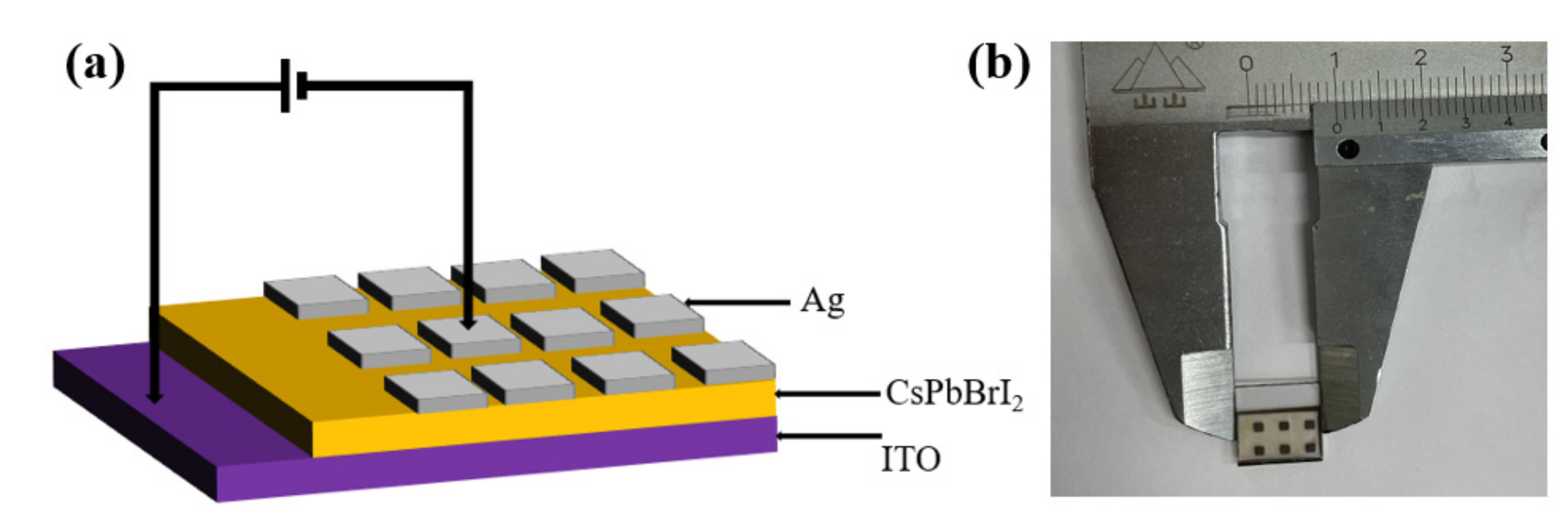
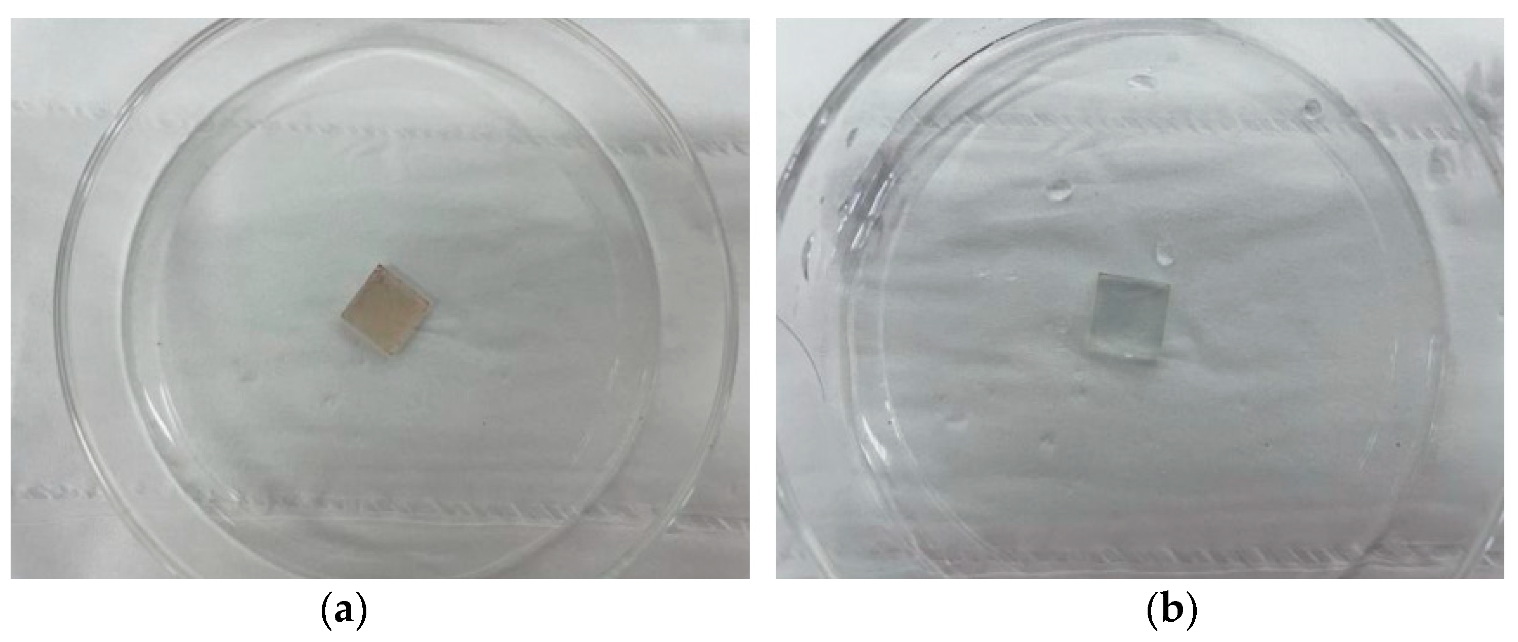
2.2. Ag/CsPbBrI2/ITO Memory Device Fabrication

The ITO glass was ultrasonically cleaned with detergent ionized water and acetone for 5 min and then placed in a drying box for drying in a nitrogen environment. Subsequently, the CsPbBrI2 perovskite precursor solution was spin-coated on the dried ITO glass at the speed of 4500 r/h for 30 s. The annealing treatment process of obtained CsPbBrI2 perovskite film, a uniform film, was carried out at 250 °C for 1 h, and then a CsPbBrI2 perovskite film was prepared. Afterward, the Ag electrode with the scale of 1 mm × 1 mm was deposited on the CsPbBrI2 perovskite film by direct current magnetron sputtering using a shadow mask to complete the Ag/CsPbBrI2/ITO resistance switch memory device [33,34].

2.3. Analysis and Characterization of Device

The field emission scanning electron microscope was used to analyze the surface morphology of the CsPbBrI2 perovskite film and the cross-sectional morphology of the Ag/CsPbBrI2/ITO device. The X-ray diffraction pattern was used to analyze the phase compositions and crystal structure of the CsPbBrI2 perovskite film. The I-V characteristics of the device were measured by using a semiconductor parameter analyzer at room temperature to test and analyze the resistance switching effect of the Ag/CsPbBrI2/ITO resistive random memory device.

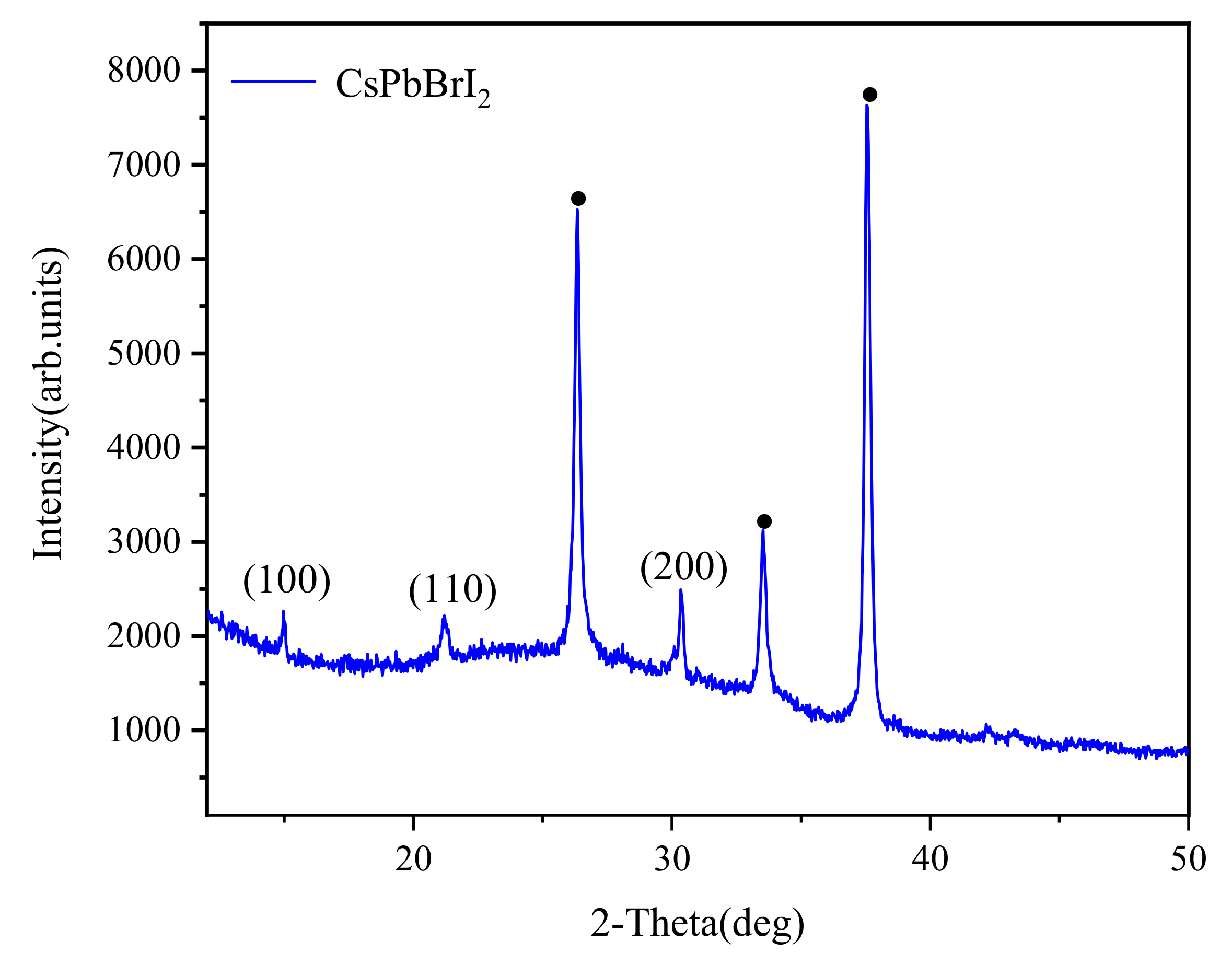
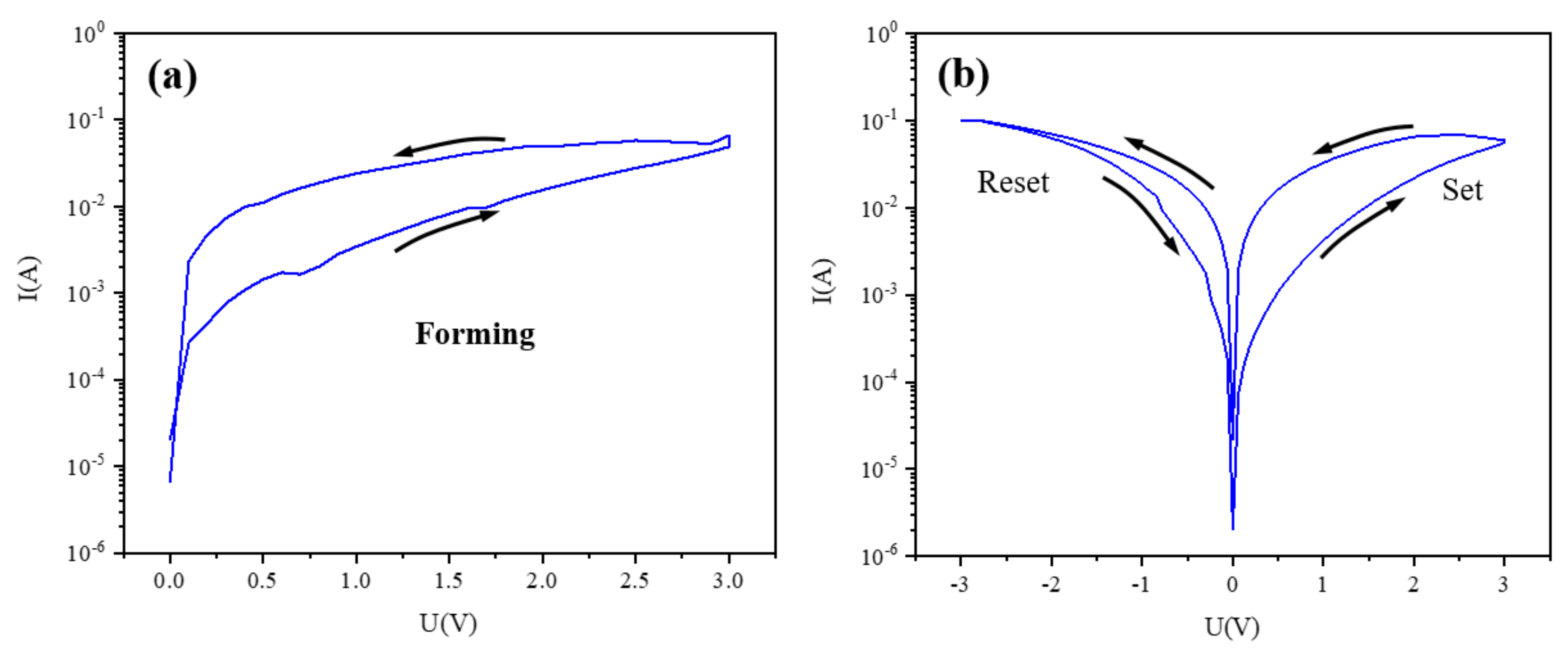
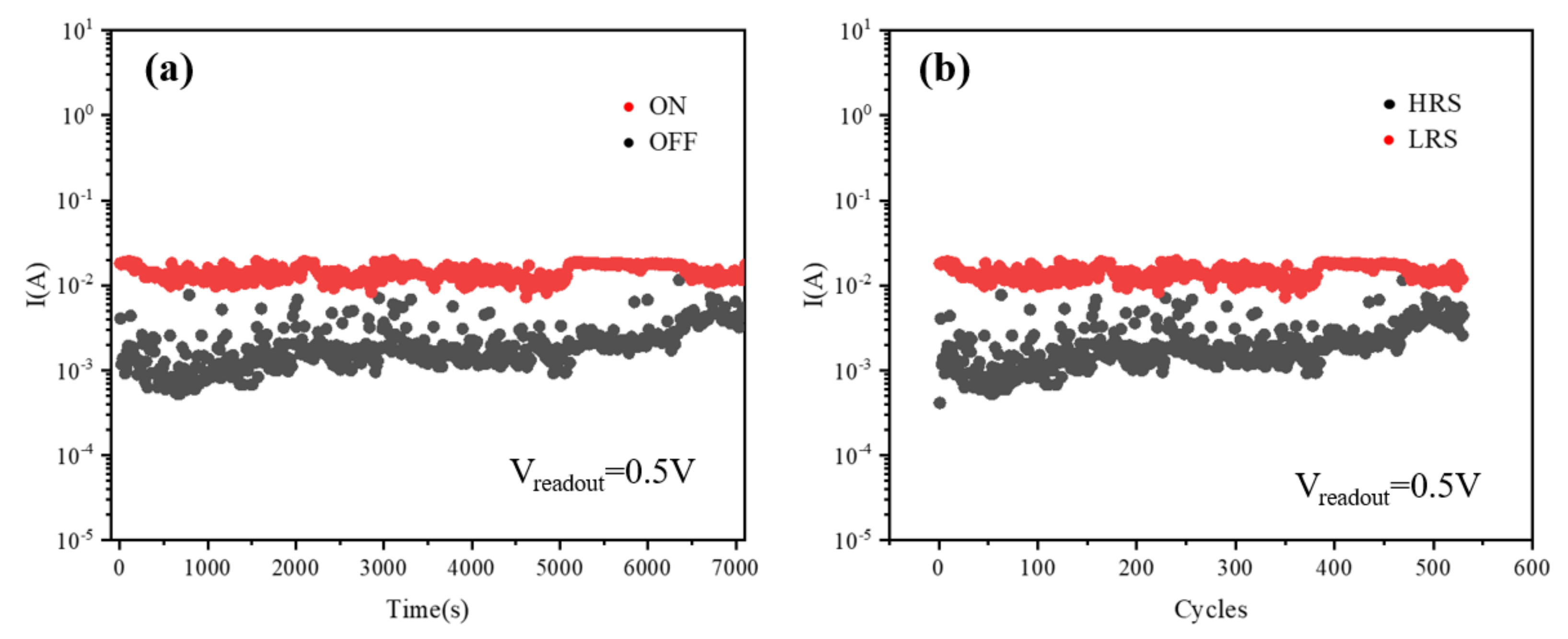
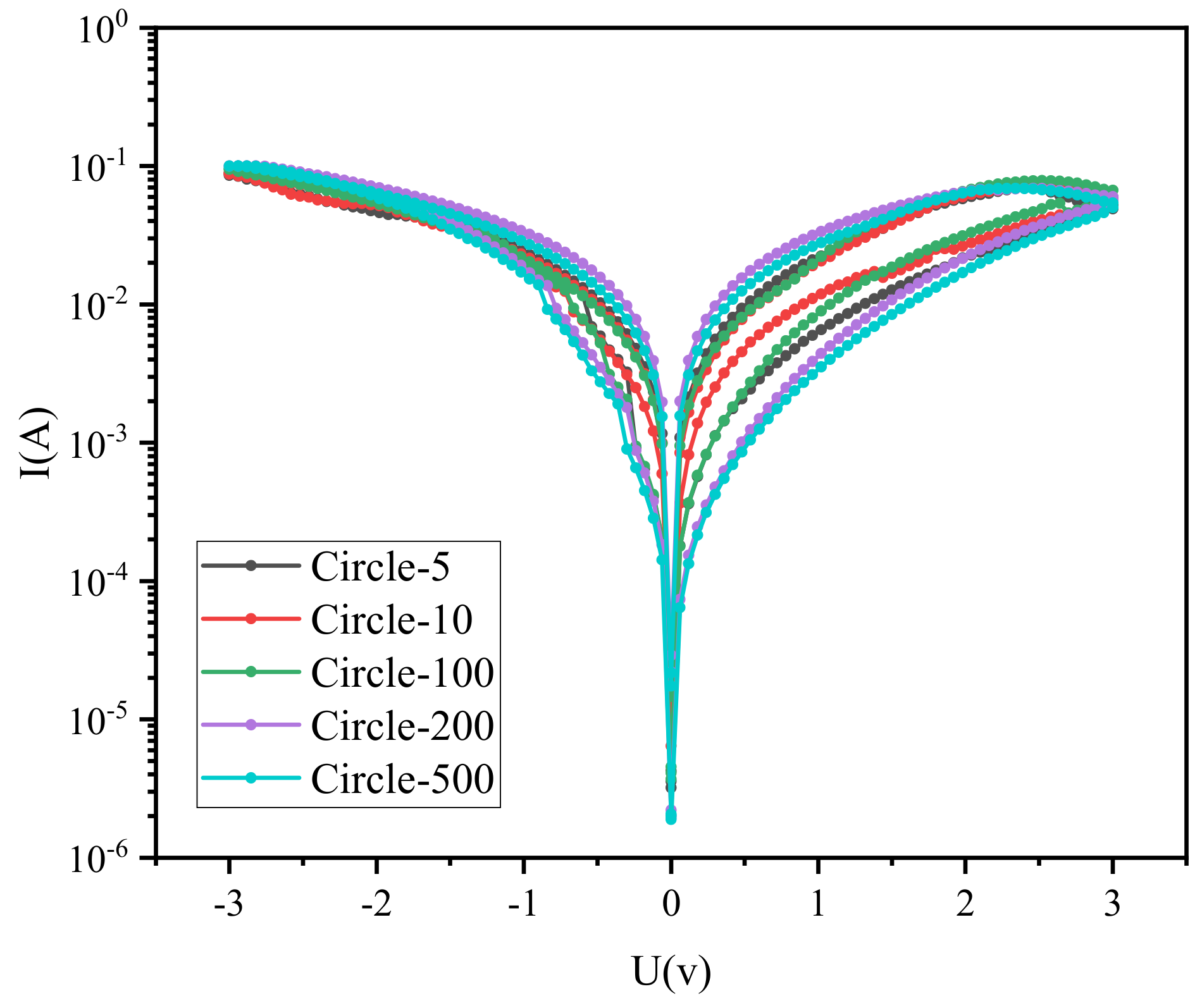
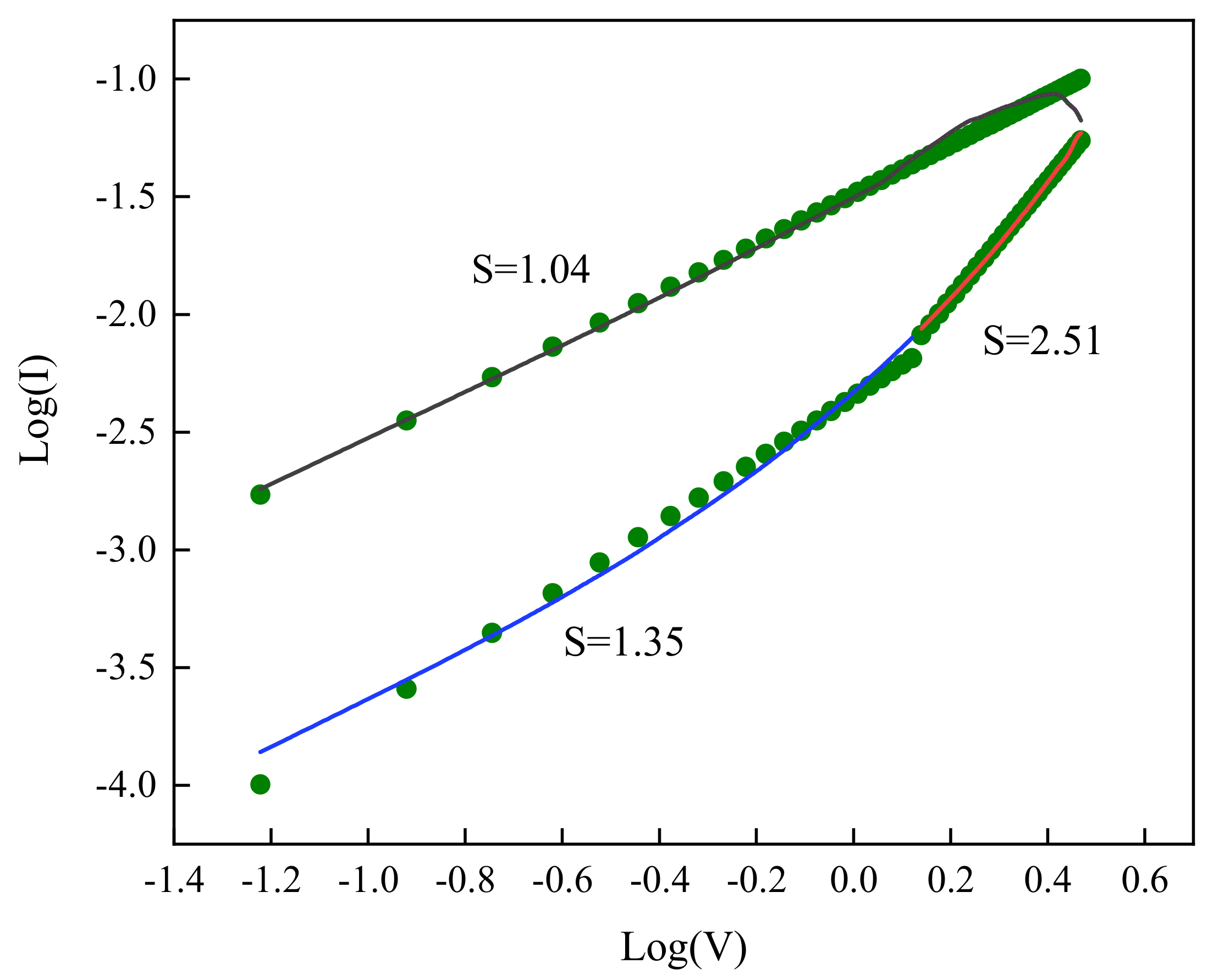
3. Results and Discussion

The schematic diagram of the Ag/CsPbBrI2/ITO resistive random memory device (a) and the optical image of the final device (b) are shown in Figure 1. The typical sandwich structure of the device can be seen from Figure 1a, in which the CsPbBrI2 film is used as the middle active layer, and Ag and ITO glass are respectively used as the upper and lower electrodes. By applying a voltage between the two electrodes, a resistance random-access memory is formed.
Figure 2 shows the scanning electron microscope surface morphology of the CsPbBrI2 perovskite film. It can be seen from Figure 2 that the particles on the film surface are uniformly distributed, it shows that the CsPbBrI2 perovskite film prepared by this experimental preparation method has good stability with the thickness of 1.5 μm, which lays the foundation for the performance of the final device [28,35]. However, the entire film is relatively less compact, which might be caused by non-optimized spin-rate control [36]. Figure 3 shows the X-ray diffraction pattern of the CsPbBrI2 film. It can be found that except for the peaks of the ITO substrate marked with black dots, all samples have strong diffraction peaks at 14.4, 20.7 and 29.4°, respectively, corresponding to the (100), (110) and (200) crystal planes of CsPbBrI2. There are also some very weak diffraction peaks that represent a small number of impurities, such as CsPbBrI2, that are not completely dissolved, and these impurities have little effect on the resistance switching behavior [37,38].
Next, we applied a cycle voltage of -3V-0V-3V on the Ag/CsPbBrI2/ITO random memory device. Figure 4a shows the initialization process of the Ag/CsPbBrI2/ITO resistance random-access memory device. At the initial moment, the device is in a high resistance state. After initialization, the device switches between high and low resistance states under the action of an external electric field [39,40]. The typical semi-logarithmic I-V curve shown in Figure 4a is obtained by cycling the voltage sweep in the following order 0 → −3.0 → 0 → 3.0 → 0V. As shown in Figure 4a, the device changes from a high resistance state (HRS) to a low resistance state (LRS) at the voltage of about 3 V for the first time as the voltage increases from 0V to 3V, the corresponding process is called the setting process and the corresponding voltage is called the setting voltage (Vset = 3 V). After this switching, the low resistance state (LRS) of the device remains until the negative voltage reaches -3V, then the resistive state of the device changes from low resistance state (LRS) to high resistance state (HRS), corresponding to the reset process, and the corresponding voltage is called reset voltage (Vreset = -3 V).
The memory device was found to exhibit stable current-voltage (I-V) characteristics after cycling the voltage sweep, which indicates that the device has a reversible resistance switch between the high resistance state (HRS) and the low resistance state (LRS). The retention characteristics of ON and OFF currents are obtained with a reading voltage (Vreadout) of 0.5 V for a time period of ∼104 s to evaluate the non-volatile properties of the Ag/CsPbBrI2/ITO memory device. Figure 5 shows the retention characteristics of on-current (ON) and off-current (OFF) when the read voltage is 0.5 V. It can be seen from Figure 5a that as time increases, the current value of the device decreases slightly, but the switching ratio between the high resistance state and the low resistance state remains relatively stable, and the on-current (ON) has been able to maintain 104 s, which indicates a reliable and reproducible resistive switching behavior in the Ag/CsPbBrI2/ITO memory device. In addition, the switching durability of the Ag/CsPbBrI2/ITO random memory device was also tested. As shown in Figure 5b, there is still a stable transition between resistance states and low resistance state of the Ag/CsPbBrI2/ITO random memory device after 500 cycles of cyclic voltage scanning, which indicates that the Ag/CsPbBrI2/ITO resistive random memory device based on the CsPbBrI2 perovskite film maintains a stable and repeatable resistance switching behavior.
In addition, I-V curves of different batches of Ag/CsPbBrI2/ITO devices tests are very important for evaluating the repeatability of Ag/CsPbBrI2/ITO resistive random memory devices. It can be seen from Figure 6 that the resistance switching behavior of three different Ag/CsPbBrI2/ITO memory devices are similar after the cyclic voltage sweep. The I-V curve of Ag/CsPbBrI2/ITO memory device after 5, 10, 100, 200, 500 cycles is shown in Figure 7. It can be seen that the resistance switching performance of the device can still maintain a stable trend after multiple cycles of voltage scanning.
In order to further understand the resistance conversion behavior of Ag/CsPbBrI2/ITO resistive random memory devices, it is necessary to deeply understand the internal physical mechanism of the resistance switching effect. The previous research mainly focuses on the conductive wire model, which is generally dominated by the ohmic conduction mechanism for the conduction mechanism of the halogen perovskite resistance switching effect. Figure 8 shows the logI–logV characteristics with the positive voltage sweep. It can be seen that the slope S of the low resistance state (LRS) is 1.04, which corresponds to the ohmic conduction mechanism. According to known research reports, iodide ions and their vacancies in perovskite iodide are the dominant factors in the formation of conductive filaments, which are mainly attributed to the relatively low migration rate and relatively low migration barrier of iodide ions [41], but there is no direct experimental evidence. Although the Ag electrodes may also play a role in the formation of conductive filaments, the thicker intermediate active layer can hinder the formation of conductive metal filaments. However, the contact barrier between the upper electrode and the intermediate active layer plays an important role in the formation of conductive filaments. The sharp increase of the current during the initialization process shows the typical feature of the conductive filament model. When the device changes from a low resistance state (LRS) to a high resistance state (HRS), the slope of the curve becomes 2.51, which conforms to the spatial conduction mechanism compared with the ohmic conduction mechanism of low resistance state (LRS). With the gradual decrease of the voltage, the slope of the curve changes from 2.51 to 1.35, and the corresponding conduction mechanism of the resistance switching effect becomes an ohmic conduction mechanism. In a complete cycle, the conduction mechanism of the device has undergone the transformation of ohmic conduction–spatial conduction–ohmic conduction [42].
In order to fully understand the resistance switching effect and its conduction mechanism of the device, the resistance switching effect of the Ag/CsPbBrI2/ITO resistive random memory device is analyzed based on the conduction mechanism [28,43]. As shown in Figure 1, When a negative voltage sweep is applied to the memory device in the HRS, iodine ions can easily migrate toward the ITO electrode with the accumulation of vacancies from top to bottom electrode along the one-dimensional channel. As the negative voltage increases, the current increases sharply, corresponding to the initialization process for the vacancies to gradually migrate to form conductive filaments. The device changes from a high resistance state (HRS) to a low resistance state (LRS) and maintains a low resistance state (LRS) until the positive voltage reaches a certain value, the device begins to transition from a low resistance state (LRS) to a high resistance state (HRS). The iodide ions begin to redistribute along with the vacancies by applying a larger positive voltage leads to rupture of the conductive filaments of the vacancies, which prompts the device to switch from the high resistance state (HRS) to the low resistance state (LRS).
In previous studies, it has been shown that some perovskite materials have transient behavior, the most representative of which is the CsPbBr3 perovskite film.In this study, it can be found that the film on the ITO surface quickly dissolved in the deionized water after 3s in Figure 9, which indicates that the Ag/CsPbBrI2/ITO resistive random memory device based on the all-inorganic halide perovskite CsPbBrI2 shows transient properties. In the future, this will be applied in short-period data storage unit devices, and implantable electronic devices with human or environmental sensors for the entire electronic devices can be degraded in deionized water to obtain completely self-damaging transient electronic devices [44,45].

4. Conclusions

In summary, the spin-coating method was used to successfully prepare CsPbBrI2 film, and a resistance random memory device with a sandwich structure of Ag/CsPbBrI2/ITO was fabricated. The surface micromorphology of CsPbBrI2 film and phase compositions were analyzed. The experimental results show that the Ag/CsPbI3/ITO memory device with high uniformity presents a non-volatile, reliable, reproducible and long-term stable resistive switching behavior of up to 500 cycles under fully open-air conditions by applying a cyclic scanning voltage to the device. The resistance switching behavior of the device is deeply analyzed by using the formation and partial fracture model of conductive filaments caused by the migration of iodide ions and the corresponding vacancies. At the same time, the transient properties of the CsPbBrI2 film that can quickly dissolve in deionized water make it potentially useful in short-period data storage units and implantable electronic devices with human or environmental sensors.

Author Contributions

W.K.: Conceptualization, Resources, Writing—original draft, Writing—review and editing, Supervision. X.Y.: Methodology, Data curation, Validation, Formal analysis. T.L.: Data curation, Project administration. All authors have read and agreed to the published version of the manuscript.

Funding

This research received no external funding.

Institutional Review Board Statement

Not applicable.

Informed Consent Statement

Not applicable.

Data Availability Statement

The raw/processed data required to reproduce these findings cannot be shared at this time as the data also forms part of an ongoing study.

Conflicts of Interest

We declare that we do not have any commercial or associative interest that represents a conflict of interest in connection with the work submitted.

References

  1. Kojima, A.; Teshima, K.; Shirai, Y.; Miyasaka, T. Organometal Halide Perovskites as Visible-Light Sensitizers for Photovoltaic Cells. J. Am. Chem. Soc. 2009, 131, 6050–6051. [Google Scholar] [CrossRef] [PubMed]
  2. Correa-Baena, J.P.; Abate, A.; Saliba, M.; Tress, W.; Jacobsson, T.J.; Grätzel, M.; Hagfeldt, A. The rapid evolution of highly efficient perovskite solar cells. Energy Environ. Sci. 2017, 10, 710–727. [Google Scholar] [CrossRef]
  3. Luo, J.M.; Lin, S.P.; Zheng, Y.; Wang, B. Nonpolar resistive switching in Mn-doped BiFeO3 thin films by chemical solution deposition. Appl. Phys. Lett. 2012, 101, 2632. [Google Scholar] [CrossRef]
  4. Yang, J.J.; Pickett, M.D.; Li, X.; Ohlberg, D.A.; Stewart, D.R.; Williams, R.S. Memristive Switching Mechanism for Meta. Nat. Nanotechnol. 2008, 3, 429–433. [Google Scholar] [CrossRef] [PubMed]
  5. Zhang, E.; Wang, W.; Zhang, C.; Jin, Y.; Zhu, G.; Sun, Q.; Zhang, D.W.; Zhou, P.; Xiu, F. Tunable charge-trap memory based on few-layer MoS2. ACS Nano 2015, 9, 612. [Google Scholar] [CrossRef] [Green Version]
  6. Rehman, S.; Khan, M.F.; Rahmani, M.K.; Kim, H.; Patil, H.; Khan, S.A.; Kang, M.H.; Kim, D.K. Neuro-Transistor Based on UV-Treated Charge Trapping in MoTe 2 for Artificial Synaptic Features. Nanomaterials 2020, 10, 2326. [Google Scholar] [CrossRef]
  7. Ji, Y.; Yang, Y.; Lee, S.-K.; Ruan, G.; Kim, T.-W.; Fei, H.; Lee, S.-H.; Kim, D.-Y.; Yoon, J.; Tour, J.M. Flexible Nanoporous WO3−x Nonvolatile Memory Device. ACS Nano 2016, 10, 7598–7603. [Google Scholar] [CrossRef]
  8. Porro, S.; Risplendi, F.; Cicero, G.; Bejtka, K.; Milano, G.; Rivolo, P.; Jasmin, A.; Chiolerio, A.; Pirri, C.F.; Ricciardi, C. Multiple Resistive Switching in Core-Shell ZnO Nanowires Exhibiting Tunable Surface States. J. Mater. Chem. C 2017, 5, 10517–10523. [Google Scholar] [CrossRef]
  9. Herpers, A.; Lenser, C.; Park, C.; Offi, F.; Borgatti, F.; Panaccione, G.; Menzel, S.; Waser, R.; Dittmann, R. Spectroscopic Proof of the Correlation between Redox-State and Charge-Carrier Transport at the Interface of Resistively Switching Ti/PCMO Devices. Adv. Mater. 2014, 26, 2730–2735. [Google Scholar] [CrossRef]
  10. Arndt, B.; Herpers, A.; Lenser, C.; Offi, F.; Borgatti, F.; Panaccione, G.; Dittmann, R.; Waser, R. Resistive switching characteristics of Pr0.48Ca0.52ManO3 heterostructures. In Proceedings of the DPG Frühjahrstagung DPG2014, Dresden, Germany, 30 March–4 April 2014. [Google Scholar]
  11. Hota, M.K.; Hedhili, M.N.; Wehbe, N.; McLachlan, M.A.; Alshareef, H.N. Multistate Resistive Switching Memory for Synaptic Memory Applications. Adv. Mater. Interfaces 2016, 3, 1600192. [Google Scholar] [CrossRef]
  12. Wang, Y.; Wu, L.; Liu, G.; Liu, L. Non-Destructive Photovoltaic Reading of Interface Type Memristors Using Graphene as Transparent Electrode. J. Alloys Compd. 2018, 740, 273–277. [Google Scholar]
  13. Guan, X.; Hu, W.; Haque, M.A.; Wei, N.; Liu, Z.; Chen, A.; Wu, T. Light-Responsive Ion-Redistribution-Induced Resistive Switching in Hybrid Perovskite Schottky Junctions. Adv. Funct. Mater. 2018, 28, 1704665. [Google Scholar] [CrossRef]
  14. Xiao, J.W.; Liu, L.; Zhang, D.; Marco, N.D.; Lee, J.W.; Lin, O.; Chen, Q.; Yang, Y. The Emergence of the Mixed Perovskites and Their Applications as Solar Cells. Adv. Energy Mater. 2017, 7, 1700491. [Google Scholar] [CrossRef]
  15. Park, Y.H.; Jeong, I.; Bae, S.; Son, H.J.; Lee, P.; Lee, J.; Lee, C.H.; Ko, M.J. Inorganic Rubidium Cation as an Enhancer for Photovoltaic Performance and Moisture Stability of HC(NH2)2PbI3 Perovskite Solar Cells. Adv. Funct. Mater. 2017, 27, 1605988. [Google Scholar] [CrossRef]
  16. Chen, H.; Xiang, S.; Li, W.; Liu, H.; Zhu, L.; Yang, S. Inorganic Perovskite Solar Cells: A Rapidly Growing Field. Sol. RRL 2018, 2, 1700188. [Google Scholar] [CrossRef]
  17. Kim, D.J.; Tak, Y.J.; Kim, W.G.; Kim, J.K.; Kim, J.H.; Kim, H.J. Resistive Switching Properties through Iodine Migrations of a Hybrid Perovskite Insulating Layer. Adv. Mater. Interfaces 2017, 4, 1601035. [Google Scholar] [CrossRef]
  18. Beal, R.E.; Slotcavage, D.J.; Leijtens, T.; Bowring, A.R.; Belisle, R.A.; Nguyen, W.H.; Burkhard, G.F.; Hoke, E.T.; McGehee, M.D. Cesium Lead Halide Perovskites with Improved Stability for Tandem Solar Cells. J. Phys. Chem. Lett. 2016, 7, 746–751. [Google Scholar] [CrossRef]
  19. Han, Y.; Meyer, S.; Dkhissi, Y.; Weber, K.; Pringle, J.M.; Bach, U.; Spiccia, L.; Cheng, Y.-B. Degradation Observations of Encapsulated Planar CH3NH3PbI3 Perovskite Solar Cells at High Temperatures and Humidity. J. Mater. Chem. A 2015, 3, 8139–8147. [Google Scholar] [CrossRef]
  20. Salado, M.; Calio, L.; Berger, R.; Kazim, S.; Ahmad, S. Influence of the Mixed Organic Cation Ratio in Lead Iodide Based Perovskite on the Performance of Solar Cells. Phys. Chem. Chem. Phys. 2016, 18, 27148–27157. [Google Scholar] [CrossRef] [Green Version]
  21. Liang, J.; Liu, J.; Jin, Z. All-Inorganic Halide Perovskites for Optoelectronics: Progress and Prospects. Sol. RRL 2017, 1, 1700086. [Google Scholar] [CrossRef]
  22. Duan, J.; Zhao, Y.; He, B.; Tang, Q. High-Purity Inorganic Perovskite Films for Solar Cells with 9.72% Efficiency. Angew. Chem. Int. Ed. 2018, 57, 3787–3791. [Google Scholar] [CrossRef]
  23. Li, Z.; Yang, M.; Park, J.-S.; Wei, S.-H.; Berry, J.J.; Zhu, K. Stabilizing Perovskite Structures by Tuning Tolerance Factor: Formation of Formamidinium and Cesium Lead Iodide Solid-State Alloys. Chem. Mater. 2016, 28, 284–292. [Google Scholar] [CrossRef]
  24. Eperon, G.E.; Paterno, G.M.; Sutton, R.J.; Zampetti, A.; Haghighirad, A.A.; Cacialli, F.; Snaith, H.J. Inorganic Caesium Lead Iodide Perovskite Solar Cells. J. Mater. Chem. A 2015, 3, 19688–19695. [Google Scholar] [CrossRef]
  25. Swarnkar, A.; Marshall, A.R.; Sanehira, E.M.; Chernomordik, B.D.; Moore, D.T.; Christians, J.A.; Chakrabarti, T.; Luther, J.M. Quantum Dot-Induced Phase Stabilization of α-CsPbI3 Perovskite for High-Efficiency Photovoltaics. Science 2016, 354, 92–95. [Google Scholar] [CrossRef] [Green Version]
  26. Liu, C.; Li, W.; Zhang, C.; Ma, Y.; Fan, J.; Mai, Y. All-Inorganic CsPbI2Br Perovskite Solar Cells with High Efficiency Exceeding 13%. J. Am. Chem. Soc. 2018, 140, 3825–3828. [Google Scholar] [CrossRef]
  27. Sutton, R.J.; Eperon, G.E.; Miranda, L.; Parrott, E.S.; Kamino, B.A.; Patel, J.B.; Hörantner, M.T.; Johnston, M.B.; Haghighirad, A.A.; Moore, D.T. Bandgap-Tunable Cesium Lead Halide Perovskites with High Thermal Stability for Efficient Solar Cell. Adv. Energy Mater. 2016, 6, 1502458. [Google Scholar] [CrossRef]
  28. Lau, C.F.J.; Deng, X.; Ma, Q.; Zheng, J.; Yun, J.S.; Green, M.A.; Huang, S.; Ho-Baillie, A.W. CsPbIBr2 Perovskite Solar Cell by Spray-Assisted Deposition. ACS Energy Lett. 2016, 1, 573–577. [Google Scholar] [CrossRef]
  29. Liu, C.; Li, W.; Chen, J.; Fan, J.; Mai, Y.; Schropp, R.E. Ultra- Thin MoOx as Cathode Buffer Layer for the Improvement of All- Inorganic CsPbIBr2 Perovskite Solar Cells. Nano Energy 2017, 41, 75–83. [Google Scholar] [CrossRef]
  30. Han, J.S.; Le, Q.V.; Choi, J.; Hong, K.; Moon, C.W.; Kim, T.L.; Kim, H.; Kim, S.Y.; Jang, H.W. Air-Stable Cesium Lead Iodide Perovskite for Ultra-Low Operating Voltage Resistive Switching. Adv. Funct. Mater. 2018, 28, 1705783. [Google Scholar] [CrossRef]
  31. Hu, Y.; Bai, F.; Liu, X.; Ji, Q.; Miao, X.; Qiu, T.; Zhang, S. Bismuth Incorporation Stabilized α-CsPbI3 for Fully Inorganic Perovskite Solar Cells. ACS Energy Lett. 2017, 2, 2219–2227. [Google Scholar] [CrossRef]
  32. Zhu, W.; Chen, D.; Zhou, L.; Zhang, C.; Chang, J.; Lin, Z.; Zhang, J.; Hao, Y. Intermediate Phase Intermolecular Exchange Triggered Defect Elimination in CH3NH3PbI3 toward Room- Temperature Fabrication of Efficient Perovskite Solar Cells. ACS Appl. Mater. Interfaces 2017, 9, 40378–40385. [Google Scholar] [CrossRef] [PubMed]
  33. Wang, J.-J.; Wang, D.-S.; Wang, J.; Zhao, W.-L.; Wang, C.-W. High Transmittance and Superhydrophilicity of Porous TiO2/SiO2 bilayer Films without UV Rrradiation. Surf. Coatings Technol. 2011, 205, 3596–3599. [Google Scholar] [CrossRef]
  34. Zhang, Z.; Ren, L.; Yan, H.; Guo, S.; Wang, S.; Wang, M.; Jin, K. Bandgap Narrowing in Bi-Doped CH3NH3PbCl3 Perovskite Single Crystals and Thin Films. J. Phys. Chem. C 2017, 121, 17436–17441. [Google Scholar] [CrossRef]
  35. Nam, J.K.; Jung, M.S.; Chai, S.U.; Choi, Y.J.; Kim, D.; Park, J.H. Unveiling the Crystal Formation of Cesium Lead Mixed-Halide Perovskites for Efficient and Stable Solar Cells. J. Phys. Chem. Lett. 2017, 8, 2936–2940. [Google Scholar] [CrossRef]
  36. Bae, D.; Palmstrom, A.; Roelofs, K.; Mei, B.; Chorkendorff, I.; Bent, S.F.; Vesborg, P.C. Tailoring Mixed-Halide, Wide-Gap Perovskites via Multistep Conversion Process. ACS Appl. Mater. Interfaces 2016, 8, 14301. [Google Scholar] [CrossRef] [Green Version]
  37. Zhu, W.; Zhang, Q.; Zhang, C.; Zhang, Z.; Chen, D.; Lin, Z.; Chang, J.; Zhang, J.; Hao, Y. Aged Precursor Solution toward Low-Temperature Fabrication of Efficient Carbon-Based All-Inorganic Planar CsPbIBr2 Perovskite Solar Cells. ACS Appl. Energy Mater. 2018, 1, 4991–4997. [Google Scholar] [CrossRef]
  38. Li, W.; Rothmann, M.U.; Liu, A.; Wang, Z.; Zhang, Y.; Pascoe, A.R.; Lu, J.; Jiang, L.; Chen, Y.; Huang, F.; et al. Phase Segregation Enhanced Ion Movement in Efficient Inorganic CsPbIBr 2 Solar Cells. Adv. Energy Mater. 2017, 7, 1700946. [Google Scholar] [CrossRef]
  39. Li, C.; Song, Z.; Zhao, D.; Xiao, C.; Subedi, B.; Shrestha, N.; Junda, M.M.; Wang, C.; Jiang, C.-S.; Al-Jassim, M.; et al. Reducing Saturation-Current Density to Realize High-Efficiency Low-Bandgap Mixed Tin-Lead Halide Perovskite Solar Cells. Adv. Energy Mater. 2019, 9, 1803135. [Google Scholar] [CrossRef]
  40. Du, Y.; Pan, H.; Wang, S.; Wu, T.; Feng, Y.P.; Pan, J.; Wee, A.T.S. Symmetrical negative differential resistance behavior of a resistive switching device. ACS Nano 2012, 6, 2517. [Google Scholar] [CrossRef]
  41. Fu, Y.J.; Xia, F.J.; Jia, Y.L.; Jia, C.J.; Li, J.Y.; Dai, X.H.; Fu, G.S.; Zhu, B.Y.; Liu, B.T. Bipolar Resistive Switching Behavior of La0.5Sr0.5CoO3−σ Films for Nonvolatile Memory Applications. Appl. Phys. Lett. 2014, 104, 223505. [Google Scholar] [CrossRef]
  42. Jing, M.; Song, W.; Chen, L.; Ma, S.; Deng, J.; Zheng, H.; Li, Y.; Liu, J.; Zhao, Z. Density Functional Theory Study of the Formaldehyde Catalytic Oxidation Mechanism on a Au-Doped CeO2(111) Surface. J. Phys. Chem. C. Nanomater. Interf. 2018, 122, 438–448. [Google Scholar]
  43. Kuan-Liang, L.; Tuo-Hung, H.; Yao-Jen, L.; Jhe-Wei, C.; Jun-Hung, L.; Jiann, S.; Cheng-Tung, C.; Tan-Fu, L.; Wen-Hsiung, C.; Wen-Yueh, J.; et al. Switching Mode and Mechanism in Binary Oxide Resistive Random Access Memory Using Ni Electrode. J. Appl. Phys. 2013, 52, 031801. [Google Scholar]
  44. Lin, Q.; Hu, W.; Zang, Z.; Zhou, M.; Du, J.; Wang, M.; Han, S.; Tang, X. Transient Resistive Switching Memory of CsPbBr3 Thin Films. Adv. Electron. Mater. 2018, 4, 1700596. [Google Scholar] [CrossRef]
  45. Chen, R.; Xu, J.; Lao, M.; Liang, Z.; Chen, Y.; Zhong, C.; Huang, L.; Hao, A.; Ismail, M. Transient Resistive Switching for Nonvolatile Memory Based on Water–Soluble Cs4PbBr6 Perovskite Films. Phys. Status Solidi RRL Rapid Res. Lett. 2019, 13, 1900397. [Google Scholar] [CrossRef]
Figure 1. The schematic diagram of the Ag/CsPbBrI2/ITO resistive random memory device (a) and the original optical image of the final device (b).
Materials 14 06629 g001
Figure 2. The scanning electron microscope surface morphology of the CsPbBrI2 perovskite film.
Materials 14 06629 g002
Figure 3. The X-ray diffraction pattern of CsPbBrI2 perovskite film.
Materials 14 06629 g003
Figure 4. The initialization process (a) and typical I-V curve (b) of the Ag/CsPbBrI2/ITO device.
Materials 14 06629 g004
Figure 5. Retention test of ON/OFF current (a) and Switching endurance between HRS and LRS (b).
Materials 14 06629 g005
Figure 6. The I-V curves of different Ag/CsPbBrI2/ITO devices.
Materials 14 06629 g006
Figure 7. The I-V curve of Ag/CsPbBrI2/ITO device after different cycles of voltage sweep.
Materials 14 06629 g007
Figure 8. The logI-logV characteristics with fitted conduction mechanism under-voltage sweeps.
Materials 14 06629 g008
Figure 9. The CsPbBrI2/ITO film before (a) and after 3s (b) in deionized water.
Materials 14 06629 g009
Publisher’s Note: MDPI stays neutral with regard to jurisdictional claims in published maps and institutional affiliations.

