
Indium-Based Micro-Bump Array Fabrication Technology with Added Pre-Reflow Wet Etching and Annealing

 , ,
, ,
Abstract
:1. Introduction
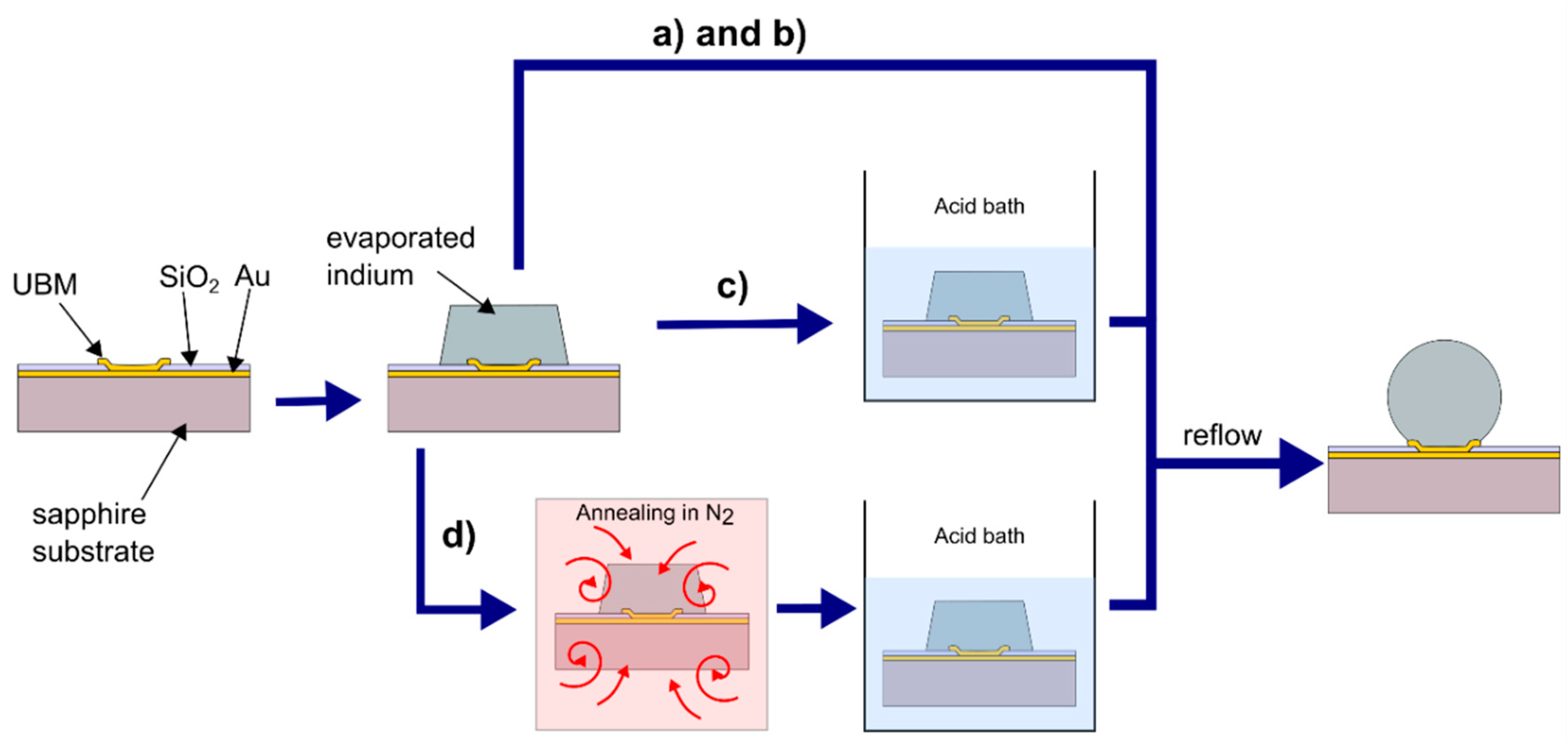
2. Experimental Procedure
2.1. Technology Stage Not Subject to Optimization
2.2. Optimized Technology Stage
- (a)
- Without pre-etching of In columns; reflow in the hydrochloric acid vapors;
- (b)
- Without pre-etching of In columns; reflow in the formic acid vapors;
- (c)
- With wet pre-etching of In columns in formic or hydrochloric acid solution; reflow in the formic acid vapors;
- (d)
- With annealing preceding the wet pre-etching of In columns in hydrochloric acid solution; reflow in the formic acid vapors.
3. Results and Discussion
4. Conclusions
Author Contributions
Funding
Institutional Review Board Statement
Informed Consent Statement
Data Availability Statement
Conflicts of Interest
References
- Rogalski, A.; Martyniuk, P.; Kopytko, M. Challenges of small-pixel infrared detectors: A review. Rep. Prog. Phys. 2016, 79, 046501. [Google Scholar] [CrossRef] [PubMed]
- Caccia, M. The challenge of hybridization. Nucl. Instrum. Methods Phys. Res. Sect. A Accel. Spectrometers Detect. Assoc. Equip. 2001, 465, 195–199. [Google Scholar] [CrossRef] [Green Version]
- Mailliart, O.; Renet, S.; Berger, F.; Gueugnot, A.; Bisotto, S.; Gout, S.; Mathieu, L.; Goiran, Y.; Chaira, T. Assembly of very fine pitches Infrared focal plane array with indium micro balls. In Proceedings of the 2019 22nd European Microelectronics and Packaging Conference & Exhibition (EMPC), Pisa, Italy, 16–19 September 2019; pp. 1–6. [Google Scholar] [CrossRef]
- Huang, Y.; Lin, C.; Ye, Z.-H.; Ding, R.-J. Reflow flip-chip bonding technology for infrared detectors. J. Micromech. Microeng. 2015, 25, 85009. [Google Scholar] [CrossRef]
- Walther, M.; Schmitz, J.; Rehm, R.; Kopta, S.; Fuchs, F.; Fleißner, J.; Cabanski, W.; Ziegler, J. Growth of InAs/GaSb short-period superlattices for high-resolution mid-wavelength infrared focal plane array detectors. J. Cryst. Growth 2005, 278, 156–161. [Google Scholar] [CrossRef]
- Breibach, J.; Lübelsmeyer, K.; Mäsing, T.; Rente, C. Development of a bump bonding interconnect technology for GaAs pixel detectors. Nucl. Instrum. Methods Phys. Res. Sect. A Accel. Spectrometers Detect. Assoc. Equip. 2001, 470, 576–582. [Google Scholar] [CrossRef]
- Huang, Q.; Xu, G.; Yuan, Y.; Cheng, X.; Luo, L. Development of indium bumping technology through AZ9260 resist electroplating. J. Micromech. Microeng. 2010, 20, 55035. [Google Scholar] [CrossRef]
- Chu, K.-M.; Lee, J.-S.; Cho, H.S.; Park, H.-H.; Jeon, D.Y. A fluxless flip chip bonding for VCSEL arrays using silver coated indium solder bumps. In Proceedings of the 2004 International IEEE Conference on the Asian Green Electronics (AGEC), Hong Kong & Shenzhen, China, 7–9 January 2004; pp. 246–253. [Google Scholar] [CrossRef]
- Kanazawa, S.; Yamazaki, H.; Nakanishi, Y.; Ueda, Y.; Kobayashi, W.; Muramoto, Y.; Ishii, H.; Sanjoh, H. 214-Gb/s 4-PAM Operation of Flip-Chip Interconnection EADFB Laser Module. J. Light. Technol. 2017, 35, 418–422. [Google Scholar] [CrossRef]
- Bah, M.A.; Manasson, A.; Outten, C.; Robinson, M.; Zhang, C.; Schumacher, J.; Desmarais, B.; Douglass, D. Indium bump deposition for flip-chip micro-array image sensing and display applications. Proc. SPIE 2018, 10639, 106392I. [Google Scholar] [CrossRef]
- Jong, J.P.; Varadaraajan, S.; Matthews, J.; Schetzina, J.F. ; Schetzina, J.F. UV detectors and focal plane array imagers based on AlGaN p-i-n photodiodes. Opto-Electron. Rev. 2002, 10, 251–260. [Google Scholar]
- Jiang, J.; Tsao, S.; O’Sullivan, T.; Razeghi, M.; Brown, G.J. Fabrication of indium bumps for hybrid infrared focal plane array applications. Infrared Phys. Technol. 2004, 45, 143–151. [Google Scholar] [CrossRef]
- Broennimann, C.; Glaus, F.; Gobrecht, J.; Heising, S.; Horisberger, M.; Horisberger, R.; Kästli, H.; Lehmann, J.; Rohe, T.; Streuli, S. Development of an Indium bump bond process for silicon pixel detectors at PSI. Nucl. Instrum. Methods Phys. Res. Sect. A Accel. Spectrometers Detect. Assoc. Equip. 2006, 565, 303–308. [Google Scholar] [CrossRef] [Green Version]
- Tian, Y.; Liu, C.; Hutt, D.; Stevens, B. Electrodeposition of indium for bump bonding. In Proceedings of the 2008 58th Electronic Components and Technology Conference, Lake Buena Vista, FL, USA, 27–30 May 2008; pp. 2096–2100. [Google Scholar] [CrossRef]
- Bergh, A.A. Atomic Hydrogen as a Reducing Agent. Bell Syst. Tech. J. 1965, 44, 261–271. [Google Scholar] [CrossRef]
- Sabat, K.C.; Rajput, P.; Paramguru, R.K.; Bhoi, B.; Mishra, B.K. Reduction of Oxide Minerals by Hydrogen Plasma: An Overview. Plasma Chem. Plasma Process. 2014, 34, 1–23. [Google Scholar] [CrossRef]
- Furuyama, K.; Yamanaka, K.; Higurashi, E.; Suga, T. Evaluation of hydrogen radical treatment for indium surface oxide removal and analysis of re-oxidation behavior. Jpn. J. Appl. Phys. 2018, 57, 02BC01. [Google Scholar] [CrossRef] [Green Version]
- Schoeller, H.; Cho, J. Oxidation and reduction behavior of pure indium. J. Mater. Res. 2009, 24, 386–393. [Google Scholar] [CrossRef]
- Huang, Y.; Lin, C.; Ye, Z.-H.; Liao, Q.-J.; Ding, R.-J. CH4/Ar/H2/SF6 Plasma Etching for Surface Oxide Removal of Indium Bumps. J. Electron. Mater. 2015, 44, 2467–2472. [Google Scholar] [CrossRef]
- Greer, F.; Dickie, M.; Vasquez, R.P.; Jones, T.J.; Hoenk, M.E.; Nikzad, S. Plasma treatment methods to improve indium bump bonding via indium oxide removal. J. Vac. Sci. Technol. B Microelectron. Nanometer Struct. 2009, 27, 2132. [Google Scholar] [CrossRef]
- Conti, F.; Hanss, A.; Fischer, C.; Elger, G. Thermogravimetric investigation on the interaction of formic acid with solder joint materials. New J. Chem. 2016, 40, 10482–10487. [Google Scholar] [CrossRef]
- Merken, P.; John, J.; Zimmermann, L.; Van Hoof, C. Technology for very dense hybrid detector arrays using electroplated indium solderbumps. IEEE Trans. Adv. Packag. 2003, 26, 60–64. [Google Scholar] [CrossRef]
- Kim, J.; Schoeller, H.; Cho, J.; Park, S. Effect of Oxidation on Indium Solderability. J. Electron. Mater. 2008, 37, 483–489. [Google Scholar] [CrossRef]
- Etching Indium to Remove Oxides. Available online: https://www.indium.com/blog/etching-indium-to-remove-oxides.php (accessed on 18 October 2021).
- Furuyama, K.; Higurashi, E.; Suga, T. Hydrogen radical treatment of printed indium solder paste for bump formation. In Proceedings of the 2017 IEEE CPMT Symposium Japan (ICSJ), Kyoto, Japan, 20–22 November 2017; pp. 157–158. [Google Scholar] [CrossRef]
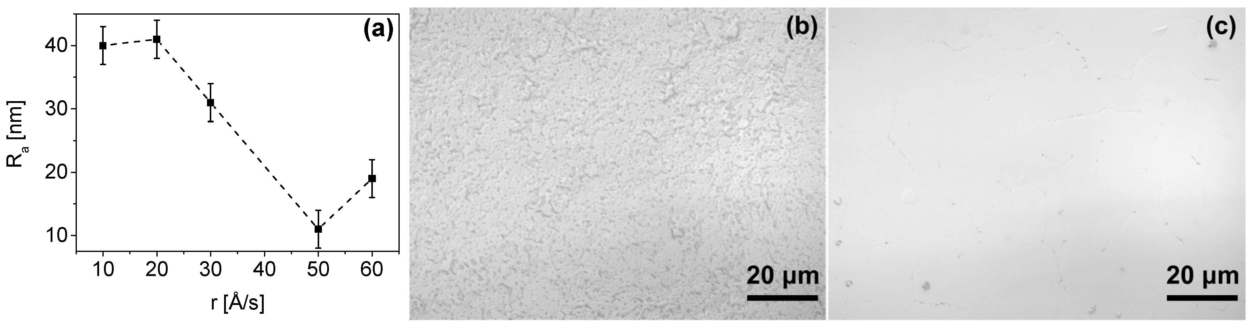
- Ruffino, F.; Grimaldi, M.G. Morphological Characteristics of Au Films Deposited on Ti: A Combined SEM-AFM Study. Coatings 2018, 8, 121. [Google Scholar] [CrossRef] [Green Version]
- Czuba, K.; Sankowska, I.; Jureńczyk, J.; Jasik, A.; Papis-Polakowska, E.; Kaniewski, J. Influence of Be doping placement in InAs/GaSb superlattice-based absorber on the performance of MWIR photodiodes. Semicond. Sci. Technol. 2017, 32, 055010. [Google Scholar] [CrossRef]
- Smoczyński, D.; Czuba, K.; Papis-Polakowska, E.; Kozłowski, P.; Ratajczak, J.; Sankowska, I.; Jasik, A. The impact of mesa etching method on IR photodetector current-voltage characteristics. Mater. Sci. Semicond. Process. 2020, 118, 105219. [Google Scholar] [CrossRef]
- Deillon, L.; Hessler, T.; Hessler-Wyser, A.; Rappaz, M. Growth of intermetallic compounds in the Au–In system: Experimental study and 1-D modelling. Acta Mater. 2014, 79, 258–267. [Google Scholar] [CrossRef] [Green Version]
- Lian, J.; Chun, S.J.W.; Goorsky, M.S.; Wang, J. Mechanical behavior of Au–In intermetallics for low temperature solder diffusion bonding. J. Mater. Sci. 2009, 44, 6155–6161. [Google Scholar] [CrossRef]
- Chiang, K.-N.; Yuan, C.-A. An overview of solder bump shape prediction algorithms with validations. IEEE Trans. Adv. Packag. 2001, 24, 158–162. [Google Scholar] [CrossRef]


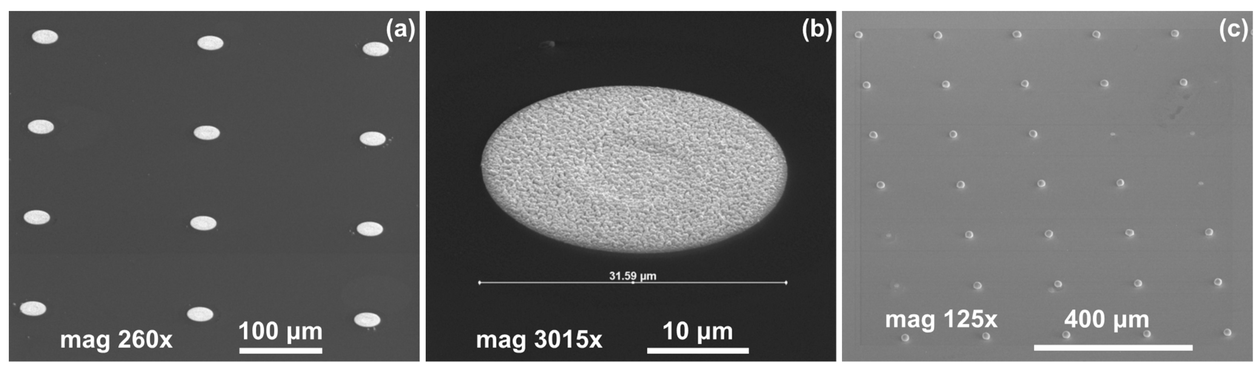
| No. | Vapor | Pre-Etching | TR [°C] | SEM Image | Comments |
|---|---|---|---|---|---|
| #1 | HCI | no | 185 | 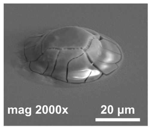 | The indium bump was not formed properly. Indium was covered with a cracked layer of indium oxide. |
| #2 | 220 | 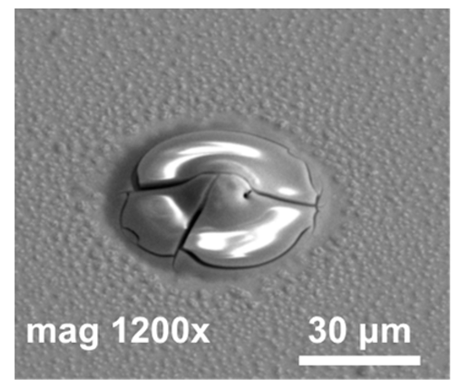 | Indium mostly evaporated. The rest was covered by a cracked oxide layer. | ||
| #3 | HCOOH | no | 185 | 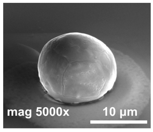 | The oxide thickness was significantly smaller than that in #1 and #2 (reflow was carried out within 20 min after removing the sample from the vacuum, in case of #1 and #2—at most 24 h). |
| #4 | HCOOH | 10% HCl | 160 |  | The indium column did not melt down completely, so the bump was not formed properly. |
| #5 | 185 | 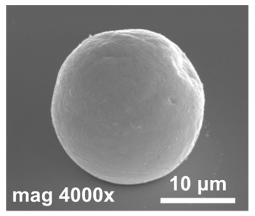 | Proper reflow process. A hyper-hemispherical indium bump with a good morphology was obtained. | ||
| #6 | 200 |  | Some of the indium evaporated, and the residue was visible as a ring. The rest melted, but a proper bump was not formed due to a lack of material. |
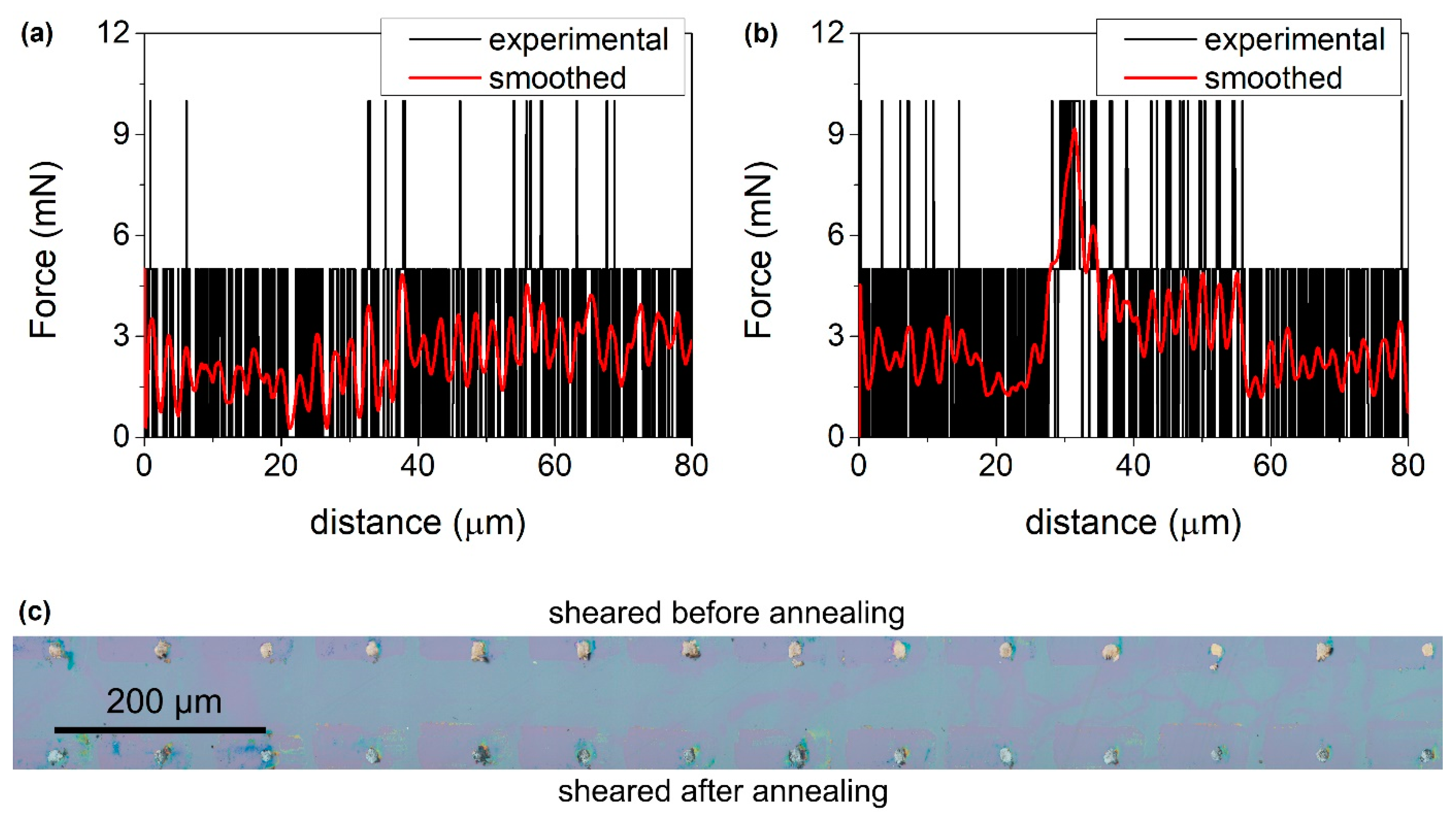
| No. | Technological Step | Introduced Change | Avg. Yield [%] |
|---|---|---|---|
| 0 | default fabrication technology | no | ~50 |
| 1 | lift-off after indium evaporation | no ultrasonic bath | ~50 |
| 2 | pre-etching of In columns | 5% HCl (20 s) | ~60 |
| 3 | additional annealing | annealing at 120 °C in nitrogen for 3 min before pre-etching in HCl | 100 |
Publisher’s Note: MDPI stays neutral with regard to jurisdictional claims in published maps and institutional affiliations. |
© 2021 by the authors. Licensee MDPI, Basel, Switzerland. This article is an open access article distributed under the terms and conditions of the Creative Commons Attribution (CC BY) license (https://creativecommons.org/licenses/by/4.0/).
Share and Cite
Kozłowski, P.; Czuba, K.; Chmielewski, K.; Ratajczak, J.; Branas, J.; Korczyc, A.; Regiński, K.; Jasik, A. Indium-Based Micro-Bump Array Fabrication Technology with Added Pre-Reflow Wet Etching and Annealing. Materials 2021, 14, 6269. https://doi.org/10.3390/ma14216269
Kozłowski P, Czuba K, Chmielewski K, Ratajczak J, Branas J, Korczyc A, Regiński K, Jasik A. Indium-Based Micro-Bump Array Fabrication Technology with Added Pre-Reflow Wet Etching and Annealing. Materials. 2021; 14(21):6269. https://doi.org/10.3390/ma14216269
Chicago/Turabian StyleKozłowski, Paweł, Krzysztof Czuba, Krzysztof Chmielewski, Jacek Ratajczak, Joanna Branas, Adam Korczyc, Kazimierz Regiński, and Agata Jasik. 2021. "Indium-Based Micro-Bump Array Fabrication Technology with Added Pre-Reflow Wet Etching and Annealing" Materials 14, no. 21: 6269. https://doi.org/10.3390/ma14216269
APA StyleKozłowski, P., Czuba, K., Chmielewski, K., Ratajczak, J., Branas, J., Korczyc, A., Regiński, K., & Jasik, A. (2021). Indium-Based Micro-Bump Array Fabrication Technology with Added Pre-Reflow Wet Etching and Annealing. Materials, 14(21), 6269. https://doi.org/10.3390/ma14216269