Article

Quantum Confinement Effect in Amorphous In–Ga–Zn–O Heterojunction Channels for Thin-Film Transistors

1
Engineering Course, Kochi University of Technology, Kami, Kochi 782-8502, Japan
2
Material Science and Engineering Course, Kochi University of Technology, Kami, Kochi 782-8502, Japan
3
Center for Nanotechnology, Research Institute, Kochi University of Technology, Kami, Kochi 782-8502, Japan
*
Author to whom correspondence should be addressed.
Materials 2020, 13(8), 1935; https://doi.org/10.3390/ma13081935
Submission received: 12 February 2020 / Revised: 30 March 2020 / Accepted: 17 April 2020 / Published: 20 April 2020

Abstract

:
Electrical and carrier transport properties in In–Ga–Zn–O thin-film transistors (IGZO TFTs) with a heterojunction channel were investigated. For the heterojunction IGZO channel, a high-In composition IGZO layer (IGZO-high-In) was deposited on a typical compositions IGZO layer (IGZO-111). From the optical properties and photoelectron yield spectroscopy measurements, the heterojunction channel was expected to have the type–II energy band diagram which possesses a conduction band offset (ΔEc) of ~0.4 eV. A depth profile of background charge density indicated that a steep ΔEc is formed even in the amorphous IGZO heterojunction interface deposited by sputtering. A field effect mobility (μFE) of bottom gate structured IGZO TFTs with the heterojunction channel (hetero-IGZO TFTs) improved to ~20 cm2 V−1 s−1, although a channel/gate insulator interface was formed by an IGZO−111 (μFE = ~12 cm2 V−1 s−1). Device simulation analysis revealed that the improvement of μFE in the hetero-IGZO TFTs was originated by a quantum confinement effect for electrons at the heterojunction interface owing to a formation of steep ΔEc. Thus, we believe that heterojunction IGZO channel is an effective method to improve electrical properties of the TFTs.

Graphical Abstract

1. Introduction

Thin-film transistors (TFTs) based on oxide semiconductors (OSs) have attracted considerable attention for next generation flat-panel displays (FPDs) due to their advantages such as high field effect mobility (μFE), steep subthreshold swing, and low leakage current [1,2,3,4,5,6,7,8,9]. Although μFE of the OS TFTs is more than an order of magnitude higher than that of hydrogenated amorphous silicon (a-Si:H) TFTs, further improvement of the μFE has been required for OS TFTs to expand their applications [9,10,11,12,13]. Optimization of compositions of the OSs is an approach to improve μFE, such as an increase of In ratio in the OSs [9,12,13,14,15]. However, it was reported the trade-off between μFE and the reliability of OS TFTs, because an increase of In ratio in the OSs leads to generation defects such as oxygen vacancies [16,17]. As another approach to improve μFE of the OSs, Koike et al. demonstrated a crystalline ZnO/ZnMgO heterojunction structure that was confirmed to be an improvement of a Hall mobility [18]. Taniguchi et al. reported a heterojunction channel consisting of polycrystalline In–Sn–O on amorphous In–Ga–Zn–O (IGZO) with a type-II energy band lineup, which attributed an improvement of the μFE to ~20 cm2 V−1 s−1 for the TFTs [19].
On the other hand, amorphous OSs have an advantage for the spatial uniformity of their transfer characteristics over a large area; thus, the amorphous OS TFTs are promising candidates for large displays. Various types of heterojunction channels, using amorphous OSs such as IGZO/In–Zn–O (IZO), Hf–In–Zn–O/IZO, Zn–Sn–O/IZO and Al–In–Zn–Sn–O/IZO, have been proposed for TFTs [20,21,22,23,24]. These heterojunction TFTs exhibited excellent μFE of over 30 cm2 V−1 s−1. The μFE improvements were mainly induced by the IZO layer, with high-μFE formed at the channel/gate insulator (GI) interface. Moreover, the heterojunction channels such as IGZO/In–Zn–O/IGZO and In–Ga–Si–O/IGZO/In–Ga–Si–O have also been reported to improve μFE [25,26]. Thus, the heterojunction channels are considered to be an appropriate approach to boost TFT performances even for amorphous OSs. However, the carrier transport properties in the heterojunction channel have not been discussed in detail, despite a key for the improvement of the μFE on the amorphous OS TFTs.
We previously reported about the IGZO TFT with a heterojunction channel consisting of different compositions of the amorphous IGZO films. Based on experimental and simulation results obtained by varying a thickness of the barrier layer of the heterojunction channel, it was found that an IGZO heterojunction channel is an effective method to independently improve electrical properties and the reliability of the TFTs [27]. However, the interface properties of the IGZO heterojunction have not been clearly understood. Furthermore, the influence of a conduction band offset (ΔEc) at the heterojunction interface on the electrical and carrier transport properties has not been analyzed in detail. Thus, it is worth to understand the steepness and ΔEc at the amorphous IGZO heterojunction interface formed by sputtering.
In this research, the electrical properties of the heterojunction IGZO TFTs were investigated by varying the thickness of a high-In IGZO (IGZO-high-In) well layer, which was deposited on a typical composition of the IGZO (IGZO-111) barrier layer for the heterojunction. In addition, formation of the heterojunction interface was considered from both of the experimental and theoretical results. μFE of the IGZO TFTs clearly increased, especially in the low gate voltage (VGS) region when the heterojunction channel was formed. From a depth analysis of the background charge density, the transition width at the heterojunction interface was estimated to be less than 3 nm. Device simulation analysis revealed that the ΔEc, which acts as a potential barrier for electrons, strongly affects carrier transport paths in the heterojunction channel, which leads to an improvement in the μFE of the TFTs.

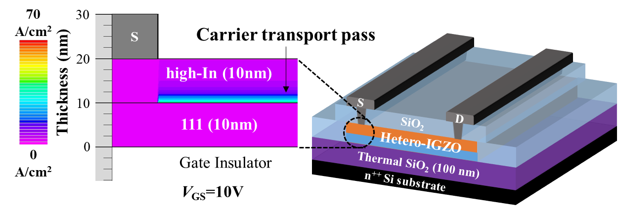
2. Experimental Methods

Figure 1a shows a schematic cross-sectional view of the bottom gate structured IGZO TFTs. The IGZO TFTs were fabricated on a heavily doped n-type Si substrate with a 100-nm-thick thermally grown SiO2. The doped n-type Si substrate and the SiO2 were used as gate electrode and GI, respectively. The IGZO channels were deposited by radio frequency (RF) magnetron sputtering without intentional substrate heating. As shown in Figure 1b,c, homogeneous channel layers of the 10-nm-thick IGZO-111 (homo-IGZO-111) and the 10-nm-thick IGZO-high-In (homo-IGZO-high-In) were separately prepared for comparison with the heterojunction channel. The oxygen flow ratio (O2/Ar + O2) during the depositions were set at 2% and 49% for the IGZO-111 and the IGZO-high-In channels, respectively. Deposition pressure and RF power for both the channels were maintained at 0.5 Pa and 4.4 W cm−2, respectively. For the heterojunction channels as shown in Figure 1d, the IGZO-high-In layer was deposited on the 10-nm-thick-IGZO-111 layer (hetero-IGZO) in a chamber without breaking the vacuum. An upper channel thickness of the IGZO-high-In layer was varied from 2.5 nm to 20 nm, while bottom channel thickness of the IGZO-111 layer was maintained at 10 nm to apply constant electric field at the heterojunction interface. Note here that the deposition conditions for each layer in the heterojunction channel were the same as the homogeneous channels. After formation of the IGZO channel using a shadow mask, a SiO2 passivation layer (200 nm) was grown by plasma-enhanced chemical vapor deposition at 180 °C using tetraethoxysilane and O2 as precursors. After opening contact holes by photolithography and dry etching, In–Sn–O source/drain electrodes were deposited by sputtering through a shadow mask. Finally, the IGZO TFTs were annealed at 350 °C in ambient air for one hour. Channel width and length were 1000 μm and 690 μm, respectively (W/L = 1000/690 μm).

3. Results and Discussion

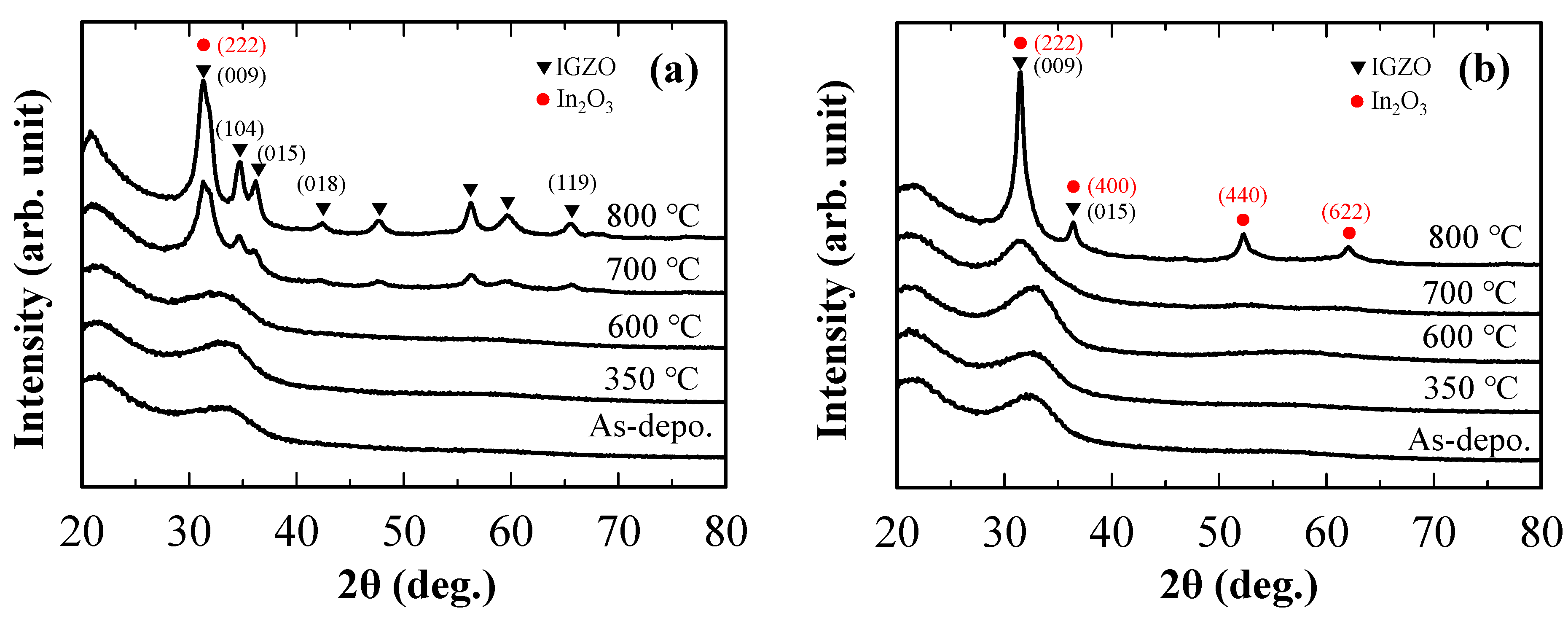
3.1. Crystallinity of IGZO films

First, the crystallinity of each IGZO layer was evaluated by grazing incidence X-ray diffraction (GIXRD, Rigaku Corp., ATX-G, Tokyo, Japan) using Cu-Kα radiation with the X-ray incident beam angle (ω) of 0.35°. Figure 2 shows GIXRD patterns of the (a) IGZO-111 and (b) IGZO-high-In layers as a function of annealing temperature. Both the IGZO-111 and high-In layer showed crystallization at the annealing temperature of 700–800 °C. The XRD peaks obtained from IGZO-111 after 800 °C attributed to crystalline IGZO, whereas that of IGZO-high-In layer mainly related to crystalline In2O3 due to high In ratio in the IGZO [28,29]. On the other hand, both the IGZO-111 and the IGZO-high-In layers retained their amorphous phase at annealing temperatures lower than 600 °C.

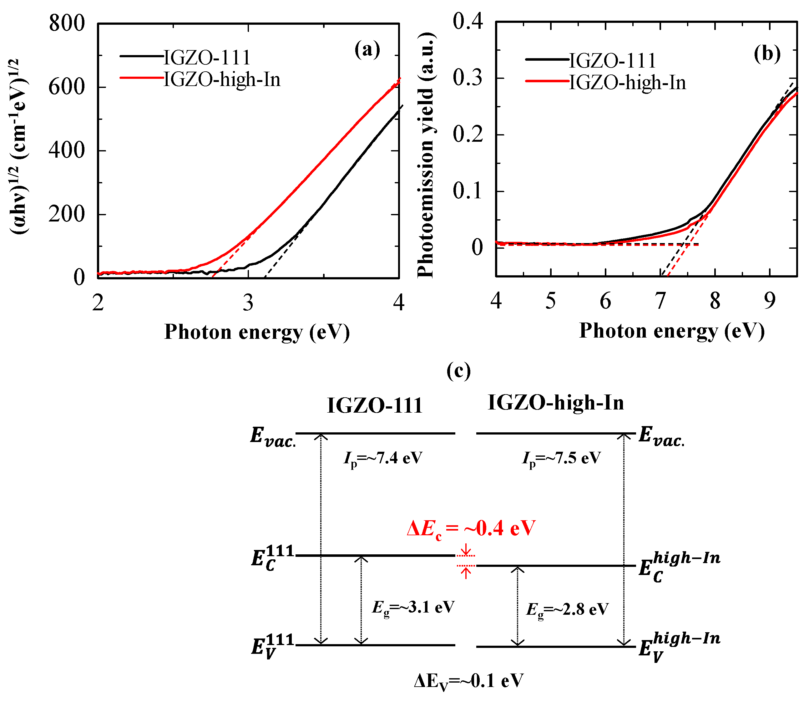
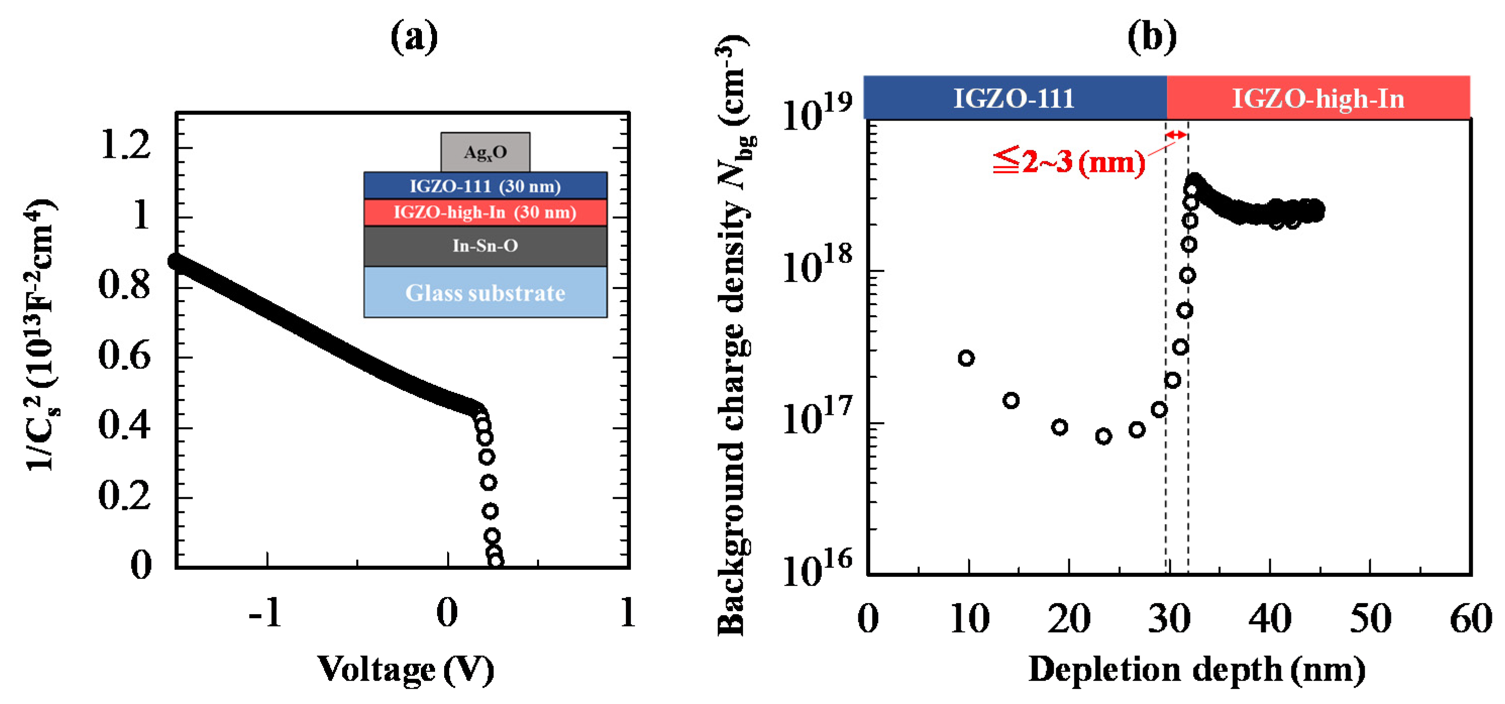
3.2. Band Alignment and Steepness at Heterojunction Interface

Optical band gap (Eg) was estimated by Tauc plot. Valence band maximum (VBM) of the IGZO films was estimated from an ionization potential (Ip), which was measured by photoelectron yield spectroscopy (Bunkoukeiki, BIP-KV202GD, Tokyo, Japan). Figure 3a,b show the Tauc plots and photoemission yield of the IGZO layers. The optical band gaps of the IGZO-111 and the IGZO-high-In layers were estimated to be ~3.1 and ~2.8 eV, respectively. VBMs of the IGZO-111 and the IGZO-high-In layers were ~7.4 and ~7.5 eV, respectively. Since conduction band minimum (CBM) of IGZO mainly consists of In-5s orbitals [30,31,32], CBM of the IGZO layer would be influence by an In ratio. From these results, the energy band diagram of the IGZO-111 and the IGZO-high-In layers was shown in Figure 3c, suggesting that a ΔEc of ~0.4 eV might be formed at the heterojunction interface.
To confirm steepness at the heterojunction interface, the depth profile of background charge density (Nbg) was evaluated by a Schottky diode (SD) with the heterojunction channel as shown in Figure 4a. Detailed fabrication process of the IGZO SD was reported elsewhere [33]. For the SD with the heterojunction channel, channel thicknesses for the each IGZO layer were set at 30 nm. Carrier density (ne) of the IGZO-111 was set at ~1 × 1017 cm−3 to obtain good Schottky contact, while that of the IGZO-high-In was set at ~3 × 1018 cm−3 to enhance the difference of Nbg at the heterojunction interface. The Nbg was estimated using an equation as shown below [34,35];
N b g = 2 q ε 0 ε s [ 1 ( 1 / C s 2 ) / V ]
where εs and Cs were permittivity and capacitance per unit area of the IGZO, respectively. The Cs was measured using Agilent E4980A LCR meter (California, CA, USA). Figure 4a shows 1/Cs2-V characteristic of the Schottky diode at 1 kHz. The 1/Cs2 values gradually decreased when the voltage applied from −1.5 to 0 V. This result indicates that the heterojunction channel was not fully depleted at the negative voltage of −1.5 V. As the voltage exceeded 0 V, the 1/Cs2 values decreased steeply.
From the 1/Cs2-V characteristic, depth profile of Nbg in the heterojunction channel was calculated as shown in Figure 4b. The Nbg of IGZO-111 layer at the depletion depth from 10 to 30 nm showed approximately 1 × 1017 cm−3, and the Nbg of IGZO-high-In steeply increased to ~2 × 1018 cm−3 when the depletion depth exceeds 30 nm. The region where the transition of Nbg occurred corresponded to the heterojunction interface region. Moreover, the transition width of Nbg at the heterojunction interface was estimated to be less than 3 nm. This result indicated that steep ΔEc would be formed at the heterojunction interface even though both the amorphous IGZO layers were deposited by sputtering.

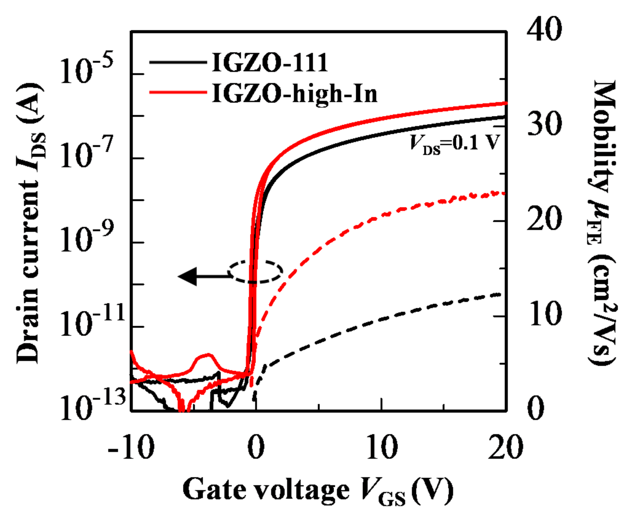
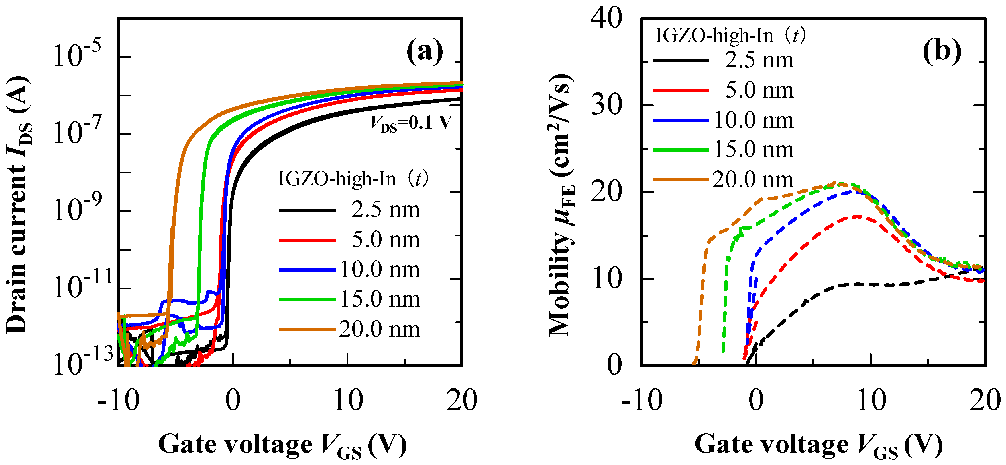
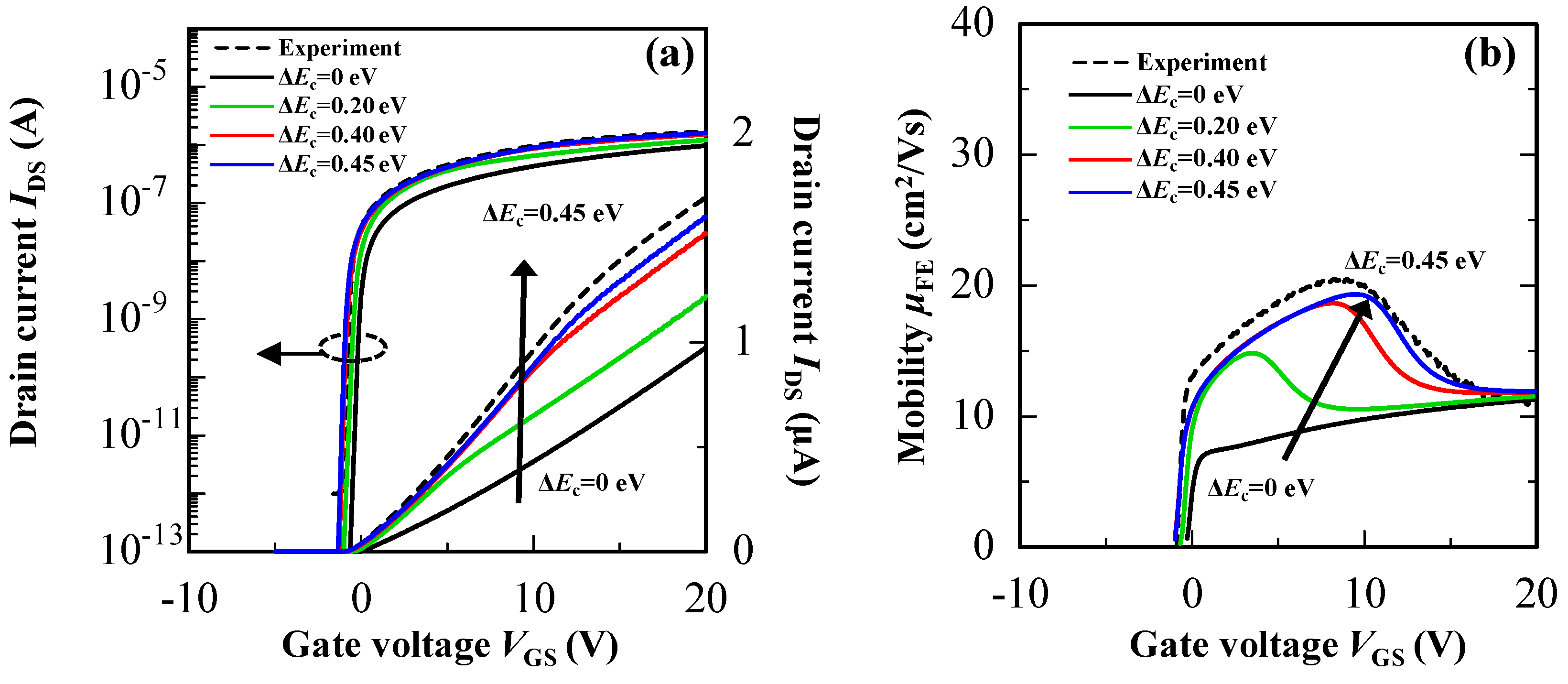
3.3. TFT Characteristics

Electrical properties of the homogeneous IGZO (homo-IGZO) TFTs were first examined as references for comparison with the heterojunction IGZO (hetero-IGZO) TFTs. Transfer characteristics of the TFTs were measured in dark using precision semiconductor parameter analyzers (Agilent 4156C and 4156A, California, CA, USA). The threshold voltage (Vth) was defined as the VGS required to obtain the drain current (IDS) of 1 nA in a linear region. The hysteresis (VH) was extracted from Vth difference between forward and reverse characteristics. The μFE was calculated from a linear region using the following equation;
μ F E = g m W L C i V D S
where gm, Ci, and VDS denote transconductance, capacitance of GI per unit area, and drain voltage, respectively.
Figure 5 shows the transfer characteristics of the homo-IGZO-111 and the IGZO-high-In TFTs. Owing to the optimization of a channel thickness and an oxygen flow ratio during the channel deposition [36,37], Vth of the homo-IGZO-111 and the IGZO-high-In TFTs were close to zero. From μFE-VGS curve shown in Figure 5, μFE of both the homo-IGZO TFTs increased with increasing VGS. The homo-IGZO-high-In TFT exhibited μFE of 22.9 cm2 V−1 s−1, which is approximately two times higher μFE than that of the homo-IGZO-111 TFT (12.4 cm2 V−1 s−1). This result indicates that μFE improvement of the homo-IGZO-high-In TFT was originated by a high-In composition, since large spherical In 5s orbitals mainly form carrier transport paths [26,30,31].
Next, electrical properties of the hetero-IGZO TFTs consisting of the IGZO-high-In on the IGZO-111 were explored. Figure 6 shows the transfer characteristic and μFE-VGS curves of the hetero-IGZO TFTs with various IGZO-high-In thicknesses. The electrical properties of the hetero-IGZO TFTs summarized in Table 1. The hetero-IGZO TFT with a 2.5-nm-thick upper IGZO-high-In layer showed a μFE of 9.9 cm2 V−1 s−1, which is almost the same μFE as homo-IGZO-111 TFT. In contrast, μFE of the hetero-IGZO TFT significantly improved to 17.2 cm2 V−1 s−1 when the upper IGZO-high-In thickness increased from 2.5 to 5.0 nm. The hetero-IGZO TFT with a 10-nm-thick upper IGZO-high-In layer exhibited a μFE of 19.6 cm2 V−1 s−1. When the upper IGZO-high-In thickness further increased to more than 10 nm, the μFE saturated to about 21 cm2 V−1 s−1, while Vth started to shift in the negative VGS direction. It can be considered that higher negative VGS is required to deplete the channel when the upper IGZO-high-In thickness increase, because the carrier density of the IGZO-high-In layer is higher than that of the IGZO-111 layer. Note here that the μFE mainly improved in low-VGS region (VGS ≦ 10 V), and it decreased to a similar value as the homo-IGZO-111 TFT at VGS of 20 V. As a result, the μFE-VGS curves showed a peak at VGS below 10 V. The μFE improvement would be caused by carrier transport in the high-In layer owing to a formation of steep ΔEc at the heterojunction interface. To understand an origin of the μFE improvement in the hetero-IGZO TFTs, carrier transport in the heterojunction channel is discussed based on the results obtained using a device simulation (Atlas, Silvaco Inc., California, CA, USA).
Meanwhile, there is no VH in the hetero-IGZO TFTs, although the homo-IGZO-high-In TFT showed VH of +1.2 V as shown in Figure 5. These results indicate that the hetero-TFTs showed high μFE with an improvement of reliability. The reliability results of the IGZO TFTs are discussed in the Figure S1 of Supplementary Information.

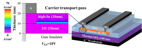
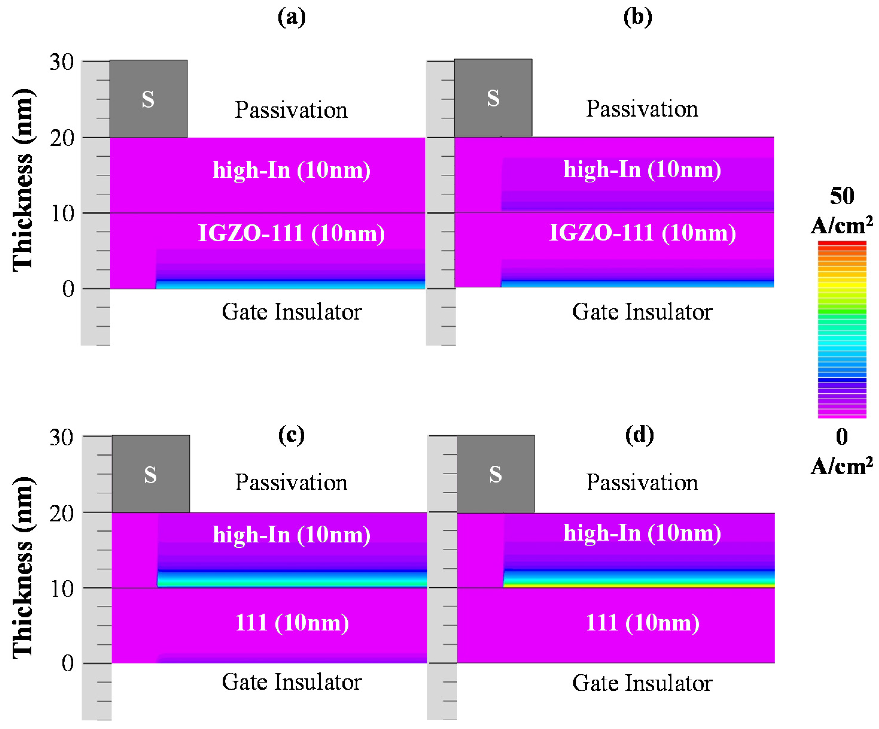
3.4. Device Simulation

To understand carrier transport in the hetero-IGZO TFTs, device simulation was carried out using device simulator, Atlas. For the model of IGZO TFTs, a ne-dependent mobility (μd) model with the density of states (DOSs) model was proposed by K. Abe [36]. The ne-dependent μd model is given by the following equations [36];
μ d = μ d 0 ( 1 + γ ) ( n e n C R )
γ = T γ T + γ 0
where μd0 is the intrinsic mobility and nCR is the critical carrier density, and γ is the index parameter.
The simulation parameters, namely, band gap, electron affinity, and ne dependences of μd were defined by the experimental results for both the IGZO layers (see Figure S2, Supplementary Information). The transfer characteristics of the homo-IGZO TFTs shown in Figure 5 were first reproduced to determine the DOSs in each IGZO layer [38,39,40]. The extracted parameters in both the IGZO models are shown in Table 2. Then, transfer characteristic of the hetero-IGZO TFT with a 10-nm-thick upper high-In layer was reproduced using the same DOSs as homo-IGZO TFTs. Note here that the contacts between S/D electrodes and IGZO back channel were assumed to be ohmic [41].
From above mentioned experimental results, the cause of the μFE improvement in the hetero-IGZO TFTs is considered to be related to a formation of ΔEc at the heterojunction interface. To prove the hypothetical origin of the μFE improvement, influence of the ΔEc on carrier transport paths of the hetero-IGZO TFT with a 10-nm-thick upper IGZO-high-In layer was analyzed by a device simulation. Figure 7a,b show transfer characteristics and μFE-VGS curves of the hetero-IGZO TFTs as a function of ΔEc formed at the heterojunction interface. The drain current and μFE of the hetero-IGZO TFTs increased with increasing the ΔEc. When the ΔEc was set at zero eV, the μFE of the hetero-IGZO TFT gradually increased with increasing VGS and showed approximately 10 cm2 V−1 s−1 at the VGS of 20 V. In contrast, the μFE in low-VGS region improved when the value of ΔEc increased. Moreover, the VGS value obtained at maximum μFE shifted to a positive VGS direction when the ΔEc increased from 0.1 to 0.45 eV. The experimental μFE-VGS curve could be reproduced well when the ΔEc was set at 0.45 eV. Thus, it was confirmed that the ΔEc at the heterojunction interface strongly influenced μFE of the hetero-IGZO TFT especially in low-VGS region.
To clarify influence of the ΔEc on carrier transport properties, drain current densities in the hetero-IGZO TFTs with different ΔEc were also analyzed by a device simulation as shown in Figure 8. The drain current densities in the hetero-IGZO TFTs were extracted at the applied VGS of 10 V and VDS of 0.1 V. For the hetero-IGZO TFT with a ΔEc of zero eV, the drain current densities increased at the IGZO−111/GI interface. Therefore, the hetero-IGZO TFT without ΔEc exhibited almost the same μFE as homo-IGZO-111 TFT. On the other hand, the drain current densities at the IGZO-111/GI interface reduced and that at the heterojunction interface increased with increasing the ΔEc. These results indicate that the carrier transport in the hetero-IGZO-TFTs changed from the IGZO-111/GI interface to the heterojunction interface owing to a quantum confinement effect for electrons when the ΔEc was formed at the heterojunction interface. Thus, the experimental and device simulation results clarified that the improvement of μFE in the hetero-IGZO TFTs was mainly caused by a quantum confinement effect for electrons, which was induced by ΔEc at the heterojunction interface.

4. Conclusions

We investigated the electrical properties of the TFTs with the IGZO heterojunction channels consisting of different compositions. The heterojunction channel was formed to deposit a high-In composition IGZO layer on an IGZO-111 layer. From band alignment analyses, type-II energy band diagram was expected to form at the heterojunction interface with a ΔEc of ~0.4 eV. In addition, a depth profile of background charge density indicated that a steep ΔEc was formed at the amorphous IGZO heterojunction interface formed by sputtering. The μFE of the IGZO TFT with the heterojunction channel improved to 20.1 cm2 V−1 s−1, and its μFE-VGS curve exhibited a maximum value at applying VGS of ~10 V. The experimental μFE-VGS curve could be reproduced well by a device simulation when the ΔEc was assumed at the heterojunction interface. Moreover, the device simulation results indicated that the carrier transport in the hetero-IGZO-TFTs changed from the IGZO-111/GI interface to the heterojunction interface owing to a quantum confinement for electrons when the ΔEc was formed at the heterojunction interface. Thus, we believe that heterojunction IGZO channel provides an effective method to improve electrical properties of the TFTs.

Supplementary Materials

The following are available online at https://www.mdpi.com/1996-1944/13/8/1935/s1, Figure S1. Changes of transfer characteristics of the (a) homo-IGZO-111, (b) homo-IGZO-high-In, and (c) hetero-IGZO TFTs as a function of PBTS time. The thickness of heterojunction channel is IGZO-high-In/IGZO-111 = 10/10 nm. (d) Relationship between μFE and ΔVth after the PBTS of 10 ks of the homo- and hetero-IGZO TFTs. The stress temperature was 60 °C and stress gate bias was +20 V, respectively, Figure S2. ne dependences of measured Hall mobilities (circles) and calculated mobilities (lines) of the IGZO-111 and the IGZO–high-In films.

Author Contributions

Conceptualization, D.K. and M.F.; methodology, D.K., S.H., Y.M. and M.F.; formal analysis, D.K. and S.H.; investigation, D.K. and S.H.; resources; M.F.; date curation; D.K., S.H., Y.M. and M.F.; writing—original draft preparation, D.K. and M.F.; writing—review and editing, D.K. and M.F.; visualization, D.K. and M.F.; supervision, M.F.; project administration, M.F.; funding acquisition, M.F. All authors have read and agreed to the published version of the manuscript.

Funding

Part of this research was funded by the JSPS KAKENHI Grant No.16K06309.

Conflicts of Interest

The authors declare no conflict of interest.

References

  1. Nomura, K.; Ohta, H.; Takagi, A.; Kamiya, T.; Hirano, M.; Hosono, H. Room-temperature fabrication of transparent flexible thin-film transistors using amorphous oxide semiconductors. Nature 2004, 432, 488–492. [Google Scholar] [CrossRef] [PubMed]
  2. Hirao, T.; Furuta, M.; Furuta, H.; Matsuda, T.; Hiramatsu, T.; Hokari, H.; Yoshida, M. 4.1: Distinguished Paper: High Mobility Top-Gate Zinc Oxide Thin-Film Transistors (ZnO-TFTs) for Active-Matrix Liquid Crystal Displays. SID Symp. Dig. Tech. Pap. 2006, 37, 18. [Google Scholar] [CrossRef]
  3. Jiang, J.; Toda, T.; Hung, M.P.; Wang, D.; Furuta, M. Highly stable fluorine-passivated In–Ga–Zn–O thin-film transistors under positive gate bias and temperature stress. Appl. Phys. Express 2014, 7, 114103. [Google Scholar] [CrossRef]
  4. Cho, S.H.; Ryu, M.K.; Kim, H.-O.; Kwon, O.S.; Park, E.-S.; Roh, Y.-S.; Hwang, C.-S.; Park, S.-H.K. Influence of gate dielectric/channel interface engineering on the stability of amorphous indium gallium zinc oxide thin-film transistors. Phys. Status solidi A 2014, 211, 2126–2133. [Google Scholar] [CrossRef]
  5. Wang, D.; Hung, M.P.; Jiang, J.; Toda, T.; Furuta, M. Suppression of Degradation Induced by Negative Gate Bias and Illumination Stress in Amorphous InGaZnO Thin-Film Transistors by Applying Negative Drain Bias. ACS Appl. Mater. Interfaces 2014, 6, 5713–5718. [Google Scholar] [CrossRef]
  6. Koretomo, D.; Toda, T.; Matsuda, T.; Kimura, M.; Furuta, M. Anomalous Increase in Field-Effect Mobility in In–Ga–Zn–O Thin-Film Transistors Caused by Dry-Etching Damage Through Etch-Stop Layer. IEEE Trans. Electron Devices 2016, 63, 2785–2789. [Google Scholar] [CrossRef]
  7. Magari, Y.; Makino, H.; Furuta, M. Carrier Generation Mechanism and Origin of Subgap States in Ar- and He-Plasma-Treated In–Ga–Zn–O Thin Films. ECS J. Solid State Sci. Technol. 2017, 6, Q101–Q107. [Google Scholar] [CrossRef]
  8. Aman, S.G.M.; Magari, Y.; Shimpo, K.; Hirota, Y.; Makino, H.; Koretomo, D.; Furuta, M. Low-temperature (150 °C) activation of Ar + O2 + H2-sputtered In–Ga–Zn–O for thin-film transistors. Appl. Phys. Express 2018, 11, 081101. [Google Scholar] [CrossRef]
  9. Kamiya, T.; Hosono, H. Material characteristics and applications of transparent amorphous oxide semiconductors. NPG Asia Mater. 2010, 2, 15–22. [Google Scholar] [CrossRef] [Green Version]
  10. Fortunato, E.; Barquinha, P.; Martins, R. Oxide Semiconductor Thin-Film Transistors: A Review of Recent Advances. Adv. Mater. 2012, 24, 2945–2986. [Google Scholar] [CrossRef]
  11. Raja, J.; Jang, K.; Nguyen, C.P.T.; Yi, J.; Balaji, N.; Hussain, S.Q.; Chatterjee, S. Improvement of Mobility in Oxide-Based Thin Film Transistors: A Brief Review. Trans. Electr. Electron. Mater. 2015, 16, 234–240. [Google Scholar] [CrossRef]
  12. Liao, C. Mobility impact on compensation performance of AMOLED pixel circuit using IGZO TFTs. J. Semicond. 2019, 40, 022403. [Google Scholar] [CrossRef]
  13. Arai, T.; Sasaoka, T. 49.1: Invited Paper: Emergent Oxide TFT Technologies for Next-Generation AM-OLED Displays. SID Symp. Dig. Tech. Pap. 2011, 42, 710–713. [Google Scholar] [CrossRef]
  14. Jang, Y.H.; Kim, D.H.; Choi, W.; Kang, M.-G.; Chun, K.I.; Jeon, J.; Ko, Y.; Choi, U.; Lee, S.-M.; Bae, J.U.; et al. 7-4: Invited Paper: Internal Compensation Type OLED Display Using High Mobility Oxide TFT. SID Symp. Dig. Tech. Pap. 2017, 48, 76–79. [Google Scholar] [CrossRef]
  15. Nomura, K.; Takagi, A.; Kamiya, T.; Ohta, H.; Hirano, M.; Hosono, H. Amorphous Oxide Semiconductors for High-Performance Flexible Thin-Film Transistors. Jpn. J. Appl. Phys. 2006, 45, 4303–4308. [Google Scholar] [CrossRef]
  16. Chong, E.; Chun, Y.S.; Lee, S.Y. Amorphous silicon–indium–zinc oxide semiconductor thin film transistors processed below 150 °C. Appl. Phys. Lett. 2010, 97, 102102. [Google Scholar] [CrossRef]
  17. Kizu, T.; Aikawa, S.; Mitoma, N.; Shimizu, M.; Gao, X.; Lin, M.F.; Nabatame, T.; Tsukagoshi, K. Low-Temperature Processable Amorphous In-WO Thin-Film Transistors with High Mobility and Stability. Appl. Phys. Lett. 2014, 104, 152103. [Google Scholar] [CrossRef]
  18. Koike, K.; Hama, K.; Nakashima, I.; Takada, G.-Y.; Ozaki, M.; Ogata, K.-I.; Sasa, S.; Inoue, M.; Yano, M. Piezoelectric Carrier Confinement by Lattice Mismatch at ZnO/Zn0.6Mg0.4O Heterointerface. Jpn. J. Appl. Phys. 2004, 43, L1372–L1375. [Google Scholar] [CrossRef]
  19. Taniguchi, S.; Yokozeki, M.; Ikeda, M.; Suzuki, T.-K. Transparent Oxide Thin-Film Transistors Using n-(In2O3)0.9(SnO2)0.1/InGaZnO4 Modulation-Doped Heterostructures. Jpn. J. Appl. Phys. 2011, 50, 04DF11. [Google Scholar] [CrossRef]
  20. Jeon, S.; Kim, S.I.; Park, S.; Song, I.; Park, J.; Kim, S.; Kim, C. Low-Frequency Noise Performance of a Bilayer InZnO–InGaZnO Thin-Film Transistor for Analog Device Applications. IEEE Electron Device Lett. 2010, 31, 1128–1130. [Google Scholar] [CrossRef]
  21. Chong, E.; Lee, S.Y. Influence of a highly doped buried layer for HfInZnO thin-film transistors. Semicond. Sci. Technol. 2011, 27, 12001. [Google Scholar] [CrossRef]
  22. Kim, H.-S.; Park, J.S.; Jeong, H.-K.; Son, K.S.; Kim, T.S.; Seon, J.-B.; Lee, E.; Chung, J.G.; Kim, D.H.; Ryu, M.; et al. Density of States-Based Design of Metal Oxide Thin-Film Transistors for High Mobility and Superior Photostability. ACS Appl. Mater. Interfaces 2012, 4, 5416–5421. [Google Scholar] [CrossRef] [PubMed]
  23. Jung, H.Y.; Kang, Y.; Hwang, A.Y.; Lee, C.K.; Han, S.; Kim, D.-H.; Bae, J.-U.; Shin, W.-S.; Jeong, J.K. Origin of the improved mobility and photo-bias stability in a double-channel metal oxide transistor. Sci. Rep. 2014, 4, 3765. [Google Scholar] [CrossRef] [Green Version]
  24. Yang, J.H.; Choi, J.H.; Cho, S.H.; Pi, J.E.; Kim, H.O.; Hwang, C.S.; Park, K.C.; Yoo, S. Highly Stable AlInZnSnO and InZnO Double-Layer Oxide Thin-Film Transistors With Mobility Over 50 cm2/V·s for High-Speed Operation. IEEE Electron Device Lett. 2018, 39, 508–511. [Google Scholar] [CrossRef]
  25. Park, J.C.; Lee, H.-N. Improvement of the Performance and Stability of Oxide Semiconductor Thin-Film Transistors Using Double-Stacked Active Layers. IEEE Electron Device Lett. 2012, 33, 818–820. [Google Scholar] [CrossRef]
  26. Saito, N.; Miura, K.; Ueda, T.; Tezuka, T.; Ikeda, K. High-Mobility and H2-Anneal Tolerant InGaSiO/InGaZnO/InGaSiO Double Hetero Channel Thin Film Transistor for Si-LSI Compatible Process. IEEE J. Electron Devices Soc. 2018, 6, 500–505. [Google Scholar] [CrossRef]
  27. Furuta, M.; Koretomo, D.; Magari, Y.; Aman, S.G.M.; Higashi, R.; Hamada, S.; Hamada, S. Heterojunction channel engineering to enhance performance and reliability of amorphous In–Ga–Zn–O thin-film transistors. Jpn. J. Appl. Phys. 2019, 58, 090604. [Google Scholar] [CrossRef]
  28. Suko, A.; Jia, J.; Nakamura, S.-I.; Kawashima, E.; Utsuno, F.; Yano, K.; Shigesato, Y. Crystallization behavior of amorphous indium–gallium–zinc-oxide films and its effects on thin-film transistor performance. Jpn. J. Appl. Phys. 2016, 55, 35504. [Google Scholar] [CrossRef]
  29. Ide, K.; Nomura, K.; Hiramatsu, H.; Kamiya, T.; Hosono, H. Structural relaxation in amorphous oxide semiconductor, a–In–Ga–Zn–O. J. Appl. Phys. 2012, 111, 073513. [Google Scholar] [CrossRef]
  30. Kim, J.; Bang, J.; Nakamura, N.; Hosono, H. Ultra-wide bandgap amorphous oxide semiconductors for NBIS-free thin-film transistors. APL Mater. 2019, 7, 022501. [Google Scholar] [CrossRef] [Green Version]
  31. Kim, J.; Hiramatsu, H.; Hosono, H.; Kamiya, T. Effects of sulfur substitution in amorphous InGaZnO4: Optical properties and first-principles calculations. J. Ceram. Soc. Jpn. 2015, 123, 537–541. [Google Scholar] [CrossRef] [Green Version]
  32. Kim, J.; Miyokawa, N.; Sekiya, T.; Ide, K.; Toda, Y.; Hiramatsu, H.; Hosono, H.; Kamiya, T. Ultrawide band gap amorphous oxide semiconductor, Ga–Zn–O. Thin Solid Films 2016, 614, 84–89. [Google Scholar] [CrossRef] [Green Version]
  33. Magari, Y.; Hashimoto, S.; Hamada, K.; Furuta, M. Low-Temperature Processed Metal-Semiconductor Field-Effect Transistor with In–Ga–Zn–O/AgOx Schottky Gate. ECS Trans. 2016, 75, 139–144. [Google Scholar] [CrossRef]
  34. Sze, S.M.; Ng, K.K. Physics of Semiconductor Devices, 3rd ed.; Wiley: New York, NY, USA, 2007. [Google Scholar]
  35. Lee, N.H.; Nomura, K.; Kamiya, T.; Hosono, H. Metal-Semiconductor Field-Effect Transistor Made Using Amorphous In-Ga-Zn-O Channel and Bottom Pt Schottky Contact Structure at 200 C. ECS Solid State Lett. 2012, 1, Q8–Q10. [Google Scholar] [CrossRef]
  36. Kamiya, T.; Hosono, H. (Invited) Roles of Hydrogen in Amorphous Oxide Semiconductor. ECS Trans. 2013, 54, 103–113. [Google Scholar] [CrossRef]
  37. Jeong, J.; Hong, Y. Debye Length and Active Layer Thickness-Dependent Performance Variations of Amorphous Oxide-Based TFTs. IEEE Trans. Electron Devices 2012, 59, 710–714. [Google Scholar] [CrossRef]
  38. Abe, K.; Sato, A.; Takahashi, K.; Kumomi, H.; Kamiya, T.; Hosono, H. Mobility- and temperature-dependent device model for amorphous In–Ga–Zn–O thin-film transistors. Thin Solid Films 2014, 559, 40–43. [Google Scholar] [CrossRef]
  39. Kamiya, T.; Nomura, K.; Hosono, H. Origins of High Mobility and Low Operation Voltage of Amorphous Oxide TFTs: Electronic Structure, Electron Transport, Defects and Doping. J. Disp. Technol. 2009, 5, 273–288. [Google Scholar] [CrossRef]
  40. Kim, Y.; Bae, M.; Kim, W.; Kong, D.; Jung, H.K.; Kim, H.; Kim, S.; Kim, D.M.; Kim, D.H. Amorphous InGaZnO Thin-Film Transistors—Part I: Complete Extraction of Density of States Over the Full Subband-Gap Energy Range. IEEE Trans. Electron Devices 2012, 59, 2689–2698. [Google Scholar] [CrossRef]
  41. Kim, S.; Jeon, Y.W.; Kim, Y.; Kong, D.; Jung, H.K.; Bae, M.-K.; Lee, J.-H.; Du Ahn, B.; Park, S.Y.; Park, J.-H.; et al. Impact of Oxygen Flow Rate on the Instability Under Positive Bias Stresses in DC-Sputtered Amorphous InGaZnO Thin-Film Transistors. IEEE Electron Device Lett. 2011, 33, 62–64. [Google Scholar] [CrossRef]
Figure 1. (a) Schematic cross-sectional view of the bottom gate structured In–Ga–Zn–O thin-film transistor (IGZO TFT). Channel structures of the (b) homogenous typical composition of the IGZO (homo-IGZO-111), (c) homogenous high-In IGZO (homo-IGZO-high-In), and (d) heterojunction IGZO (hetero-IGZO).
Materials 13 01935 g001
Figure 2. Grazing incidence X-ray diffraction (GIXRD) patterns of (a) IGZO-111 and (b) IGZO-high-In layers as a function of annealing temperature. Annealing was carried out in air for one hour.
Materials 13 01935 g002
Figure 3. (a) Tauc plots and (b) photoemission yield of the IGZO-111 and the IGZO-high-In layers after annealing at 350 °C in in ambient air for one hour. (c) Energy band diagrams of the IGZO-111 and the IGZO-high-In layers.
Materials 13 01935 g003
Figure 4. (a) 1/Cs2-V characteristic of the Schottky diode at 1 kHz. Inset is a schematic cross-sectional view of the Schottky diode with the heterojunction IGZO. The heterojunction IGZO was annealed at 350 °C in ambient air for one hour before deposition of an AgxO electrode. (b) Depth profile of Nbg calculated using the 1/Cs2-V characteristic. The depth x = 0 nm corresponds to the AgxO/IGZO-111 interface.
Materials 13 01935 g004
Figure 5. Transfer characteristics of the homo-IGZO-111 and the IGZO-high-In TFTs (VDS = 0.1 V, W/L = 1000/690 μm).
Materials 13 01935 g005
Figure 6. (a) Transfer characteristics and (b) μFE-VGS curves of the hetero-IGZO TFTs with various thickness of the IGZO-high-In layer (VDS = 0.1 V, W/L = 1000/690 μm).
Materials 13 01935 g006
Figure 7. Simulation results of (a) transfer characteristics and (b) μFE-VGS curves of the hetero-IGZO TFTs with different ΔEc. The broken line is an experimental result of the hetero-IGZO TFT.
Materials 13 01935 g007
Figure 8. Drain current densities in the hetero-IGZO TFTs with ΔEc of the (a) 0 eV, (b) 0.2 eV, (c) 0.4 eV, and (d) 0.45 eV. The insert is the color coding for the drain current density at VGS = +10 V (VDS = 0.1 V).
Materials 13 01935 g008
Table 1. Summary of electrical properties of the hetero-IGZO TFTs with the various IGZO-high-In thicknesses.
IGZO-High-In Thickness2.5 nm5 nm10 nm15 nm20 nm
IGZO-111 Thickness10 nm
μFE (cm2 V−1 s−1)9.917.219.621.821.3
S.S. (V/dec.)0.100.100.100.120.15
Vth (V)0−0.9−0.9−3.3−5.1
VH (V)0.00.00.00.00.0
Table 2. Extracted parameters in the homo-IGZO-111 and the IGZO-high-In models.
SymbolValue (IGZO)UnitDescription
−111-High-In
NC5.0 × 10185.0 × 1018cm−3Effective conduction band density of states
μd01430cm2 V−1 s−1Intrinsic electron mobility
nCR1.0 × 10201.0 × 1020cm−3Critical electron density
Tγ178.4178.4Kγ temperature
γ0−0.31−0.31Gamma at 1/T = 0
Wga0.71.2eVDecay energy of acceptor-like Gaussian trap
Wgd0.120.12eVDecay energy of donor-like Gaussian trap
Ega00eVMean energy of Gaussian acceptor-like trap
Egd2.62.2eVMean energy of Gaussian donor-like trap
Nga1.5 × 10171.5 × 1017cm−3 ev−1Peak density of Gaussian acceptor-like trap
Ngd1.3 × 10171.3 × 1017cm−3 ev−1Peak density of Gaussian donor-like trap
Nta1.0 × 10191.0 × 1019cm−3 ev−1Acceptor-like tail trap density
Ntd3.0 × 10193.0 × 1019cm−3 ev−1Donor-like tail trap density
Wta0.010.01eVSlope of acceptor-like tail trap
Wtd0.10.1eVSlope of donor-like tail trap

