Electron Concentration Limit in Ge Doped by Ion Implantation and Flash Lamp Annealing


 ,
, 
Abstract
1. Introduction
2. Materials and Methods
3. Results
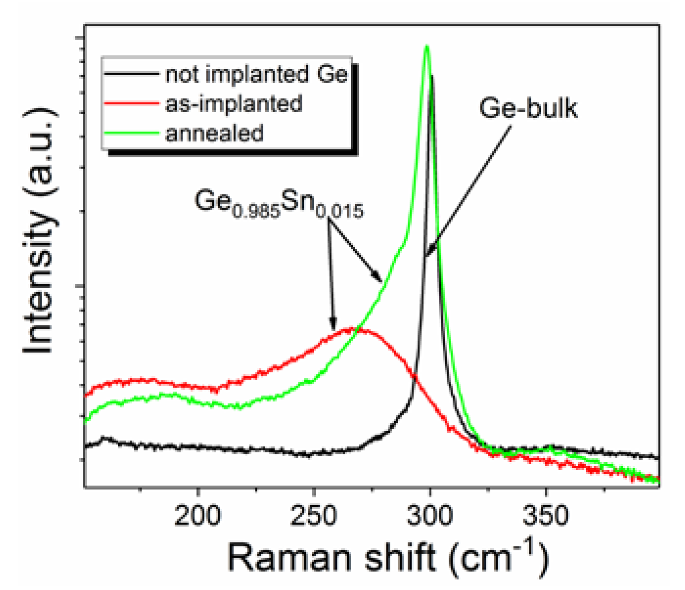
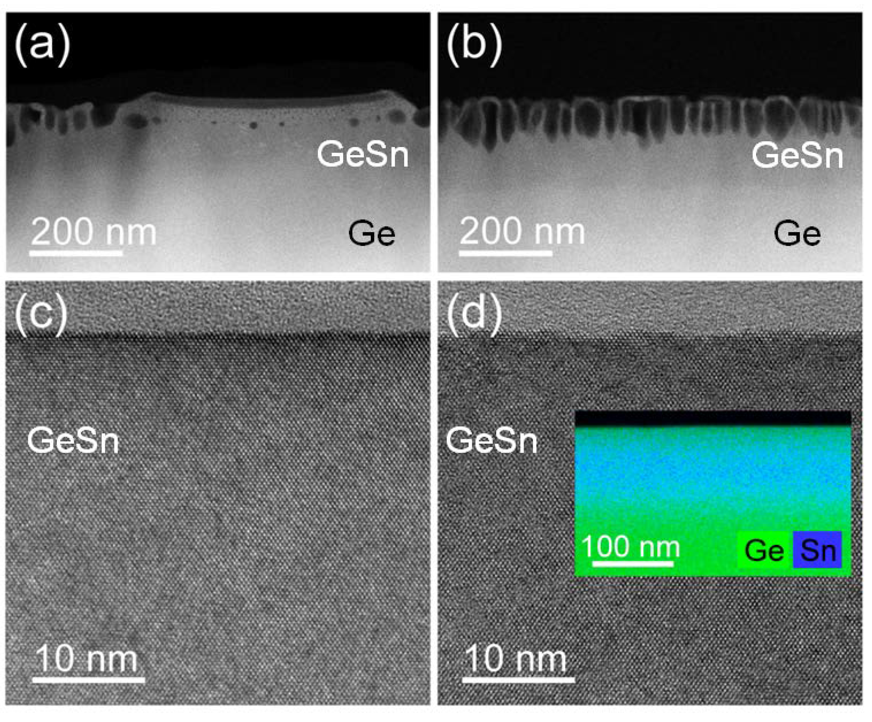
3.1. Microstructural Properties
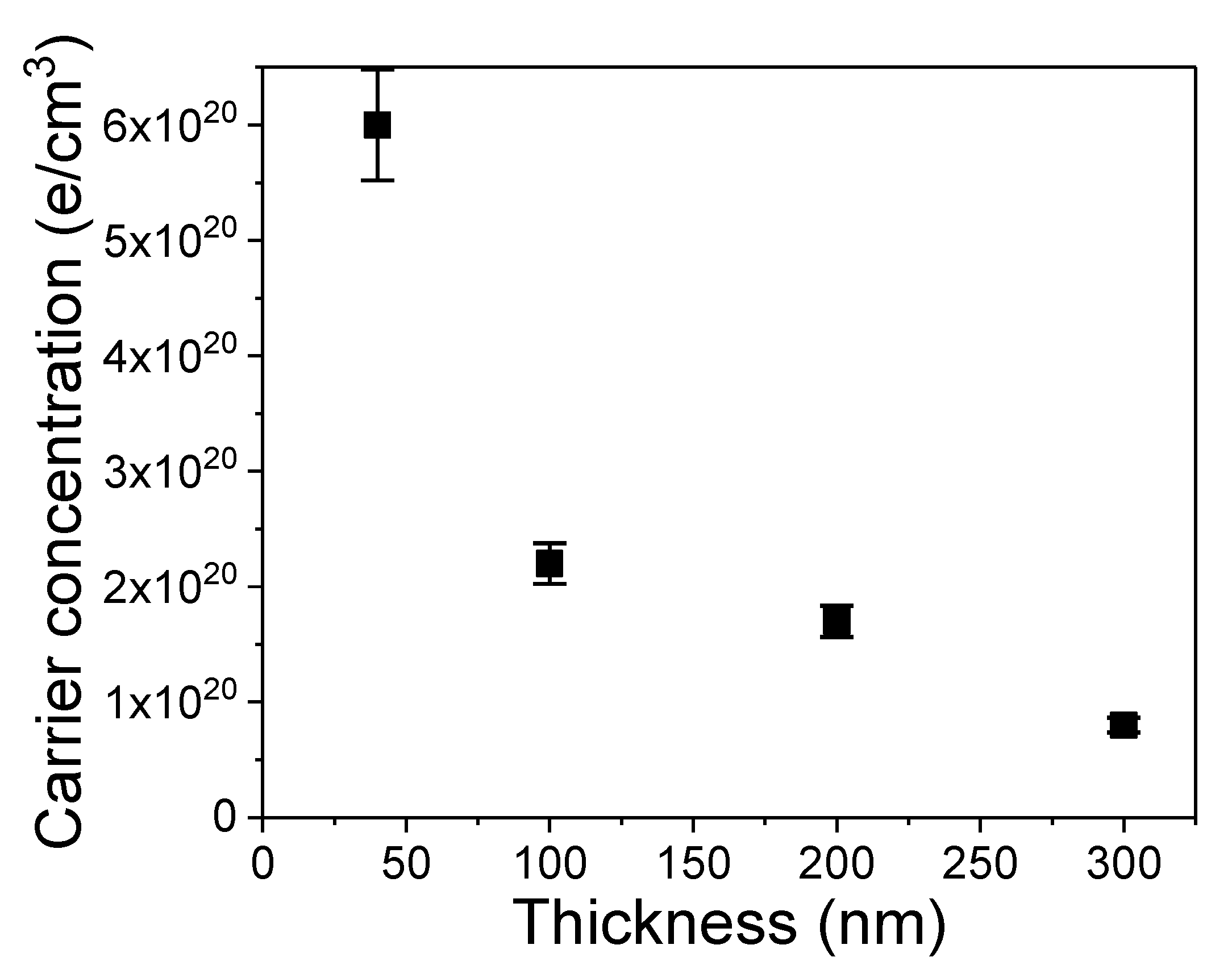
3.2. Optical and Electrical Properties
4. Conclusions
Author Contributions
Funding
Acknowledgments
Conflicts of Interest
References
- 2015 International Technology Roadmap for Semiconductors (ITRS). Available online: https://www.semiconductors.org/main/2015_international_technology_roadmap_for_semiconductors_itrs/ (accessed on 5 January 2015).
- Liu, J.; Kimerling, L.C.; Michel, J. Monolithic Ge-on-Si lasers for large-scale electronic–photonic integration. Semicond. Sci. Technol. 2012, 27, 094006. [Google Scholar] [CrossRef]
- Chaisakul, P.; Marris-Morini, D.; Frigerio, J.; Chrastina, D.; Rouifed, M.-S.; Cecchi, S.; Crozat, P.; Isella, G.; Vivien, L. Integrated germanium optical interconnects on silicon substrates. Nat. Photon. 2014, 8, 482. [Google Scholar] [CrossRef]
- Herrmannsdörfer, T.; Heera, V.; Ignatchik, O.; Uhlarz, M.; Mücklich, A.; Posselt, M.; Reuther, H.; Schmidt, B.; Heinig, K.-H.; Skorupa, W.; et al. Superconducting State in a Gallium-Doped Germanium Layer at Low Temperatures. Phys. Rev. Lett. 2009, 102, 217003. [Google Scholar] [CrossRef] [PubMed]
- Fiedler, J.; Heera, V.; Skrotzki, R.; Herrmannsdörfer, T.; Voelskow, M.; Mücklich, A.; Facsko, S.; Reuther, H.; Perego, M.; Heinig, K.-H.; et al. Superconducting Ga-overdoped Ge layers capped with SiO2: Structural and transport investigations. Phys. Rev. B 2012, 85, 134530. [Google Scholar] [CrossRef]
- Prucnal, S.; Heera, V.; Hübner, R.; Wang, M.; Mazur, G.P.; Grzybowski, M.J.; Qin, X.; Yuan, Y.; Voelskow, M.; Skorupa, W.; et al. Superconductivity in single-crystalline aluminum- and gallium-hyperdoped germanium. Phys. Rev. Mater. 2019, 3, 054802. [Google Scholar] [CrossRef]
- Prucnal, S.; Liu, F.; Voelskow, M.; Vines, L.; Rebohle, L.; Lang, D.; Berencén, Y.; Andric, S.; Boettger, R.; Helm, M.; et al. Ultra-doped n-type germanium thin films for sensing in the mid-infrared. Sci. Rep. 2016, 6, 27643. [Google Scholar] [CrossRef]
- Gallacher, K.; Velha, P.; Paul, D.J.; MacLaren, I.; Myronov, M.; Leadley, D.R. Ohmic contacts to n-type germanium withlow specific contact resistivity. Appl. Phys. Lett. 2012, 100, 022113. [Google Scholar] [CrossRef]
- Xu, C.; Kouvetakis, J.; Menéndez, J. Doping dependence of the optical dielectric function in n-type germanium. J. Appl. Phys. 2019, 125, 085704. [Google Scholar] [CrossRef]
- Milazzo, R.; Impellizzeri, G.; Piccinotti, D.; De Salvador, D.; Portavoce, A.; La Magna, A.; Fortunato, G.; Mangelinck, D.; Privitera, V.; Carnera, A.; et al. Low temperature deactivation of Ge heavily n-type doped by ion implantation and laser thermal annealing. Appl. Phys. Lett. 2017, 110, 011905. [Google Scholar] [CrossRef]
- Prucnal, S.; Berencén, Y.; Wang, M.; Georgiev, Y.M.; Erbe, A.; Khan, M.B.; Boettger, R.; Hübner, R.; Schönherr, T.; Kalbacova, J.; et al. Nanoscale n++-p junction formation in GeOI probed by tip-enhanced Raman spectroscopy and conductive atomic force microscopy. J. Appl. Phys. 2019, 125, 245703. [Google Scholar] [CrossRef]
- Mattoni, G.; Klesse, W.M.; Capellini, G.; Simmons, M.Y.; Scappucci, G. Phosphorus Molecules on Ge(001): A Playground for Controlled n-Doping of Germanium at High Densities. ACS Nano 2013, 7, 11310–11316. [Google Scholar] [CrossRef] [PubMed]
- Kujala, J.; Südkamp, T.; Slotte, J.; Makkonen, I.; Tuomisto, F.; Bracht, H. Vacancy-donor complexes in highly n-type Ge doped with As, P and Sb. J. Phys. Condens. Matter 2016, 28, 335801. [Google Scholar] [CrossRef]
- Chroneos, A.; Grimes, R.W.; Uberuaga, B.P.; Bracht, H. Diffusion and defect reactions between donors, C, and vacancies in Ge. II. Atomistic calculations of related complexes. Phys. Rev. B 2008, 77, 235208. [Google Scholar] [CrossRef]
- Chroneos, A. Dopant-defect interactions in Ge: Density functional theory calculations. Mater. Sci. Semicond. Process. 2012, 15, 691–696. [Google Scholar] [CrossRef]
- Chroneos, A.; Bracht, H. Diffusion of n-type dopants in germanium. Appl. Phys. Rev. 2014, 1, 011301. [Google Scholar] [CrossRef]
- Tran, T.T.; Alkhaldi, H.S.; Gandhi, H.H.; Pastor, D.; Huston, L.Q.; Wong-Leung, J.; Aziz, M.J.; Williams, J.S. Suppression of ion-implantation induced porosity in germanium by a silicon dioxide capping layer. Appl. Phys. Lett. 2016, 109, 082106. [Google Scholar] [CrossRef]
- Ziegler, J.F.; Ziegler, M.D.; Biersack, J.P. SRIM—The stopping and range of ions in matter. Nucl. Instrum. Methods B 2010, 268, 1818. [Google Scholar] [CrossRef]
- Doolittle, L.R. Algorithms for the rapid simulation of Rutherford backscattering spectra. Nucl. Instrum. Methods B 1985, 9, 344. [Google Scholar] [CrossRef]
- Prucnal, S.; Rebohle, L.; Skorupa, W. Doping by flash lamp annealing. Mater. Sci. Semicond. Process. 2017, 62, 115–127. [Google Scholar] [CrossRef]
- Johannes, A.; Noack, S.; Wesch, W.; Glaser, M.; Lugstein, A.; Ronning, C. Anomalous Plastic Deformation and Sputtering of Ion Irradiated Silicon Nanowires. Nano Lett. 2015, 15, 3800–3807. [Google Scholar] [CrossRef]
- Ou, X.; Keller, A.; Helm, M.; Fassbender, J.; Facsko, S. Reverse Epitaxy of Ge: Ordered and Faceted Surface Patterns. Phys. Rev. Lett. 2013, 111, 016101. [Google Scholar] [CrossRef] [PubMed]
- Prucnal, S.; Berencén, Y.; Wang, M.; Rebohle, L.; Böttger, R.; Fischer, I.A.; Augel, L.; Oehme, M.; Schulze, J.; Voelskow, M.; et al. Ex situ n+ doping of GeSn alloys via non-equilibrium processing. Semicond. Sci. Technol. 2018, 33, 065008. [Google Scholar] [CrossRef]
- Gao, K.; Prucnal, S.; Huebner, R.; Baehtz, C.; Skorupa, I.; Wang, Y.; Skorupa, W.; Helm, M.; Zhou, S. Ge1−xSnx alloys synthesized by ion implantation and pulsed laser melting. Appl. Phys. Lett. 2014, 105, 042107. [Google Scholar] [CrossRef]
- Prucnal, S.; Berencén, Y.; Wang, M.; Grenzer, J.; Voelskow, M.; Hübner, R.; Yamamoto, Y.; Scheit, A.; Bärwolf, F.; Zviagin, V.; et al. Strain and Band-Gap Engineering in Ge-Sn Alloys via P Doping. Phys. Rev. Appl. 2018, 10, 064055. [Google Scholar] [CrossRef]
- Fano, U. Effects of Configuration Interaction on Intensities and Phase Shifts. Phys. Rev. 1961, 124, 1866–1878. [Google Scholar] [CrossRef]
- Fukata, N.; Sato, K.; Mitome, M.; Bando, Y.; Sekiguchi, T.; Kirkham, M.; Hong, J.-I.; Wang, Z.L.; Snyder, R.L. Doping and Raman Characterization of Boron and Phosphorus Atoms in Germanium Nanowires. ACS Nano 2010, 4, 3807–3816. [Google Scholar] [CrossRef]
- Vohra, A.; Khanam, A.; Slotte, J.; Makkonen, I.; Pourtois, G.; Loo, R.; Vandervorst, W. Evolution of phosphorus-vacancy clusters in epitaxial germanium. J. Appl. Phys. 2019, 125, 025701. [Google Scholar] [CrossRef]


© 2020 by the authors. Licensee MDPI, Basel, Switzerland. This article is an open access article distributed under the terms and conditions of the Creative Commons Attribution (CC BY) license (http://creativecommons.org/licenses/by/4.0/).
Share and Cite
Prucnal, S.; Żuk, J.; Hübner, R.; Duan, J.; Wang, M.; Pyszniak, K.; Drozdziel, A.; Turek, M.; Zhou, S. Electron Concentration Limit in Ge Doped by Ion Implantation and Flash Lamp Annealing. Materials 2020, 13, 1408. https://doi.org/10.3390/ma13061408
Prucnal S, Żuk J, Hübner R, Duan J, Wang M, Pyszniak K, Drozdziel A, Turek M, Zhou S. Electron Concentration Limit in Ge Doped by Ion Implantation and Flash Lamp Annealing. Materials. 2020; 13(6):1408. https://doi.org/10.3390/ma13061408
Chicago/Turabian StylePrucnal, Slawomir, Jerzy Żuk, René Hübner, Juanmei Duan, Mao Wang, Krzysztof Pyszniak, Andrzej Drozdziel, Marcin Turek, and Shengqiang Zhou. 2020. "Electron Concentration Limit in Ge Doped by Ion Implantation and Flash Lamp Annealing" Materials 13, no. 6: 1408. https://doi.org/10.3390/ma13061408
APA StylePrucnal, S., Żuk, J., Hübner, R., Duan, J., Wang, M., Pyszniak, K., Drozdziel, A., Turek, M., & Zhou, S. (2020). Electron Concentration Limit in Ge Doped by Ion Implantation and Flash Lamp Annealing. Materials, 13(6), 1408. https://doi.org/10.3390/ma13061408