Ion-Locking in Solid Polymer Electrolytes for Reconfigurable Gateless Lateral Graphene p-n Junctions

 , ,
, ,
Abstract
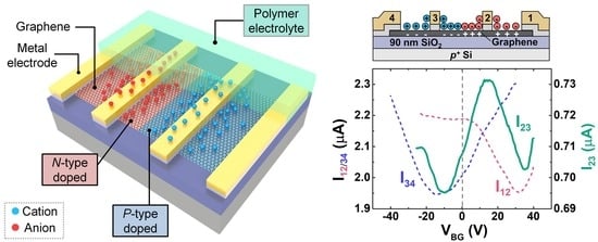
1. Introduction
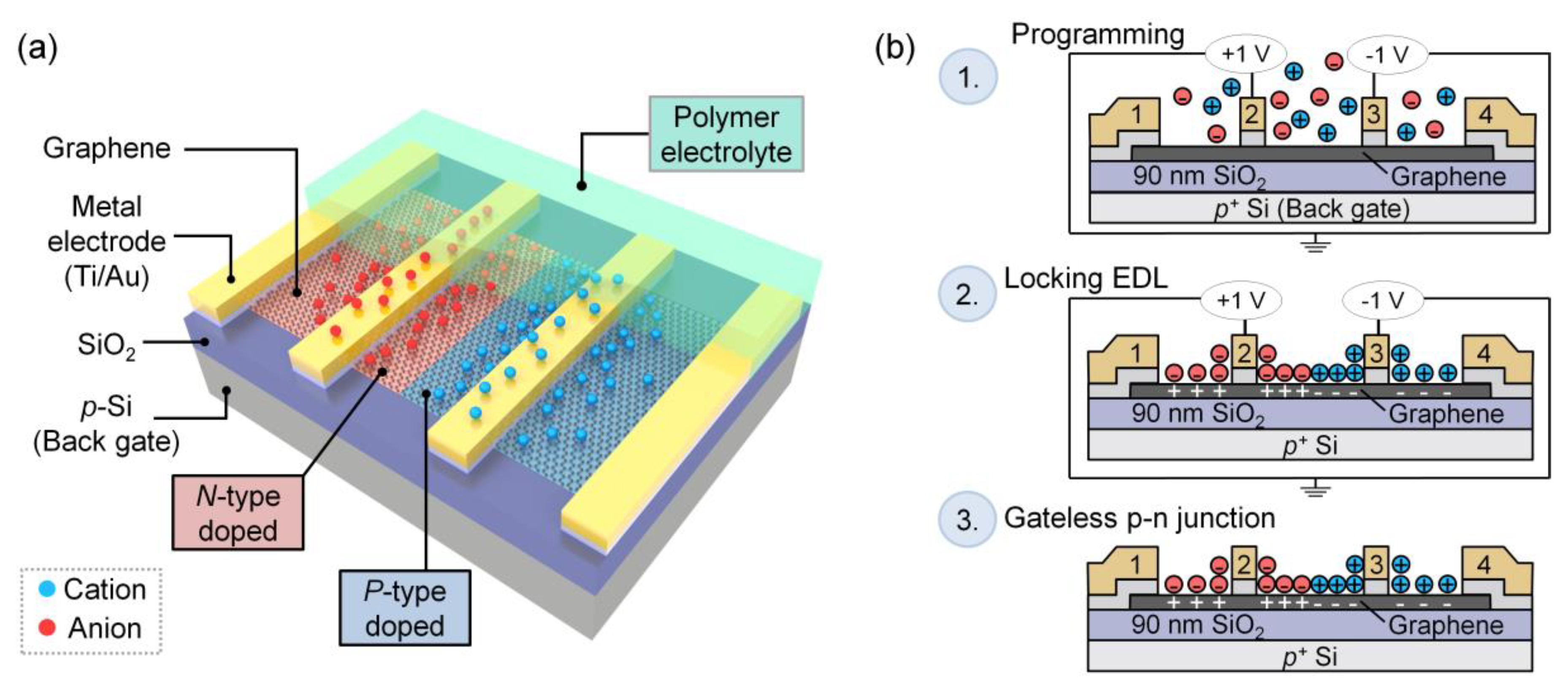
2. Materials and Methods
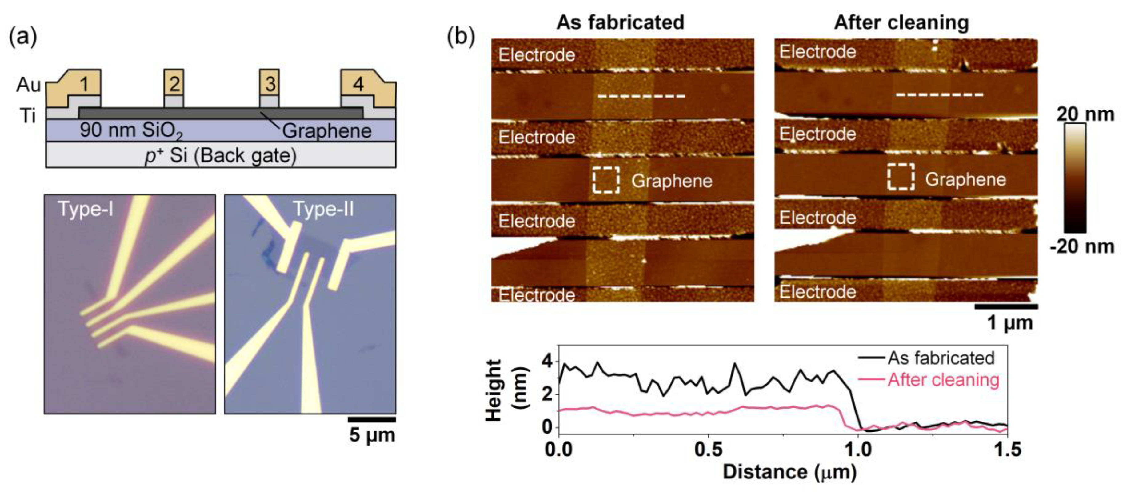
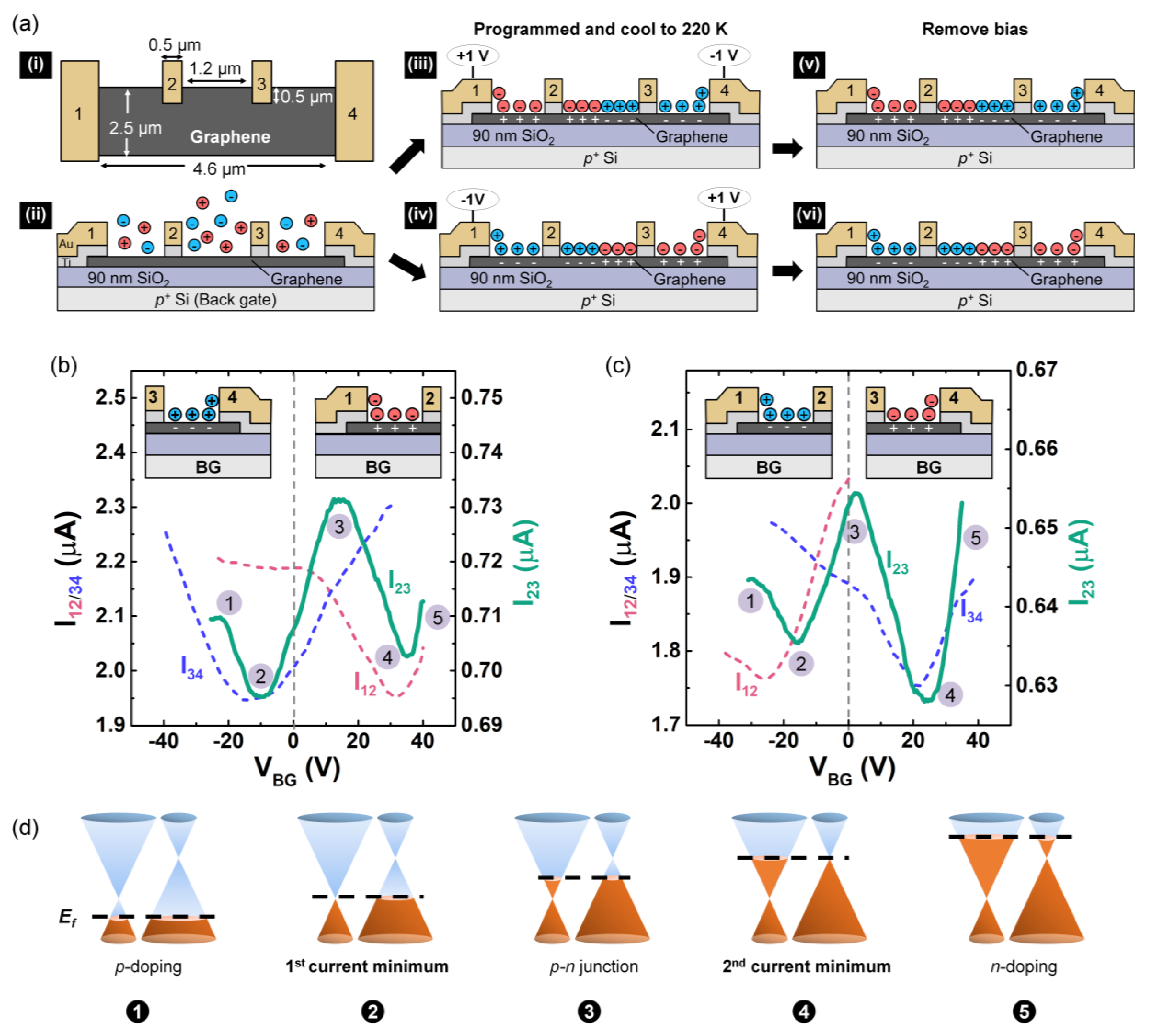
2.1. Device Fabrication
2.2. Electrolyte Preparation
2.3. P-n Junction Formation
3. Results and Discussions
3.1. P-n Junction Formation Using PEO:CsClO4
3.2. P-n Junction Formation Using DPIL
4. Conclusions
Supplementary Materials
Author Contributions
Funding
Acknowledgments
Conflicts of Interest
References
- Chiu, H.Y.; Perebeinos, V.; Lin, Y.M.; Avouris, P. Controllable P-N Junction Formation in Monolayer Graphene Using Electrostatic Substrate Engineering. Nano Lett. 2010, 10, 4634–4639. [Google Scholar] [CrossRef] [PubMed]
- Frisenda, R.; Molina-Mendoza, A.J.; Mueller, T.; Castellanos-Gomez, A.; Van Der Zant, H.S.J. Atomically Thin P-N Junctions Based on Two-Dimensional Materials. Chem. Soc. Rev. 2018, 47, 3339–3358. [Google Scholar] [CrossRef]
- Kim, S.; Shin, D.H.; Kim, C.O.; Kang, S.S.; Kim, J.M.; Jang, C.W.; Joo, S.S.; Lee, J.S.; Kim, J.H.; Choi, S.H.; et al. Graphene P-N Vertical Tunneling Diodes. ACS Nano 2013, 7, 5168–5174. [Google Scholar] [CrossRef] [PubMed]
- Novoselov, K.S.; Geim, A.K.; Morozov, S.V.; Jiang, D.; Zhang, Y.; Dubonos, S.V.; Grigorieva, I.V.; Firsov, A.A. Electric Field in Atomically Thin Carbon Films. Science 2004, 306, 666–669. [Google Scholar] [CrossRef] [PubMed]
- Bhimanapati, G.R.; Lin, Z.; Meunier, V.; Jung, Y.; Cha, J.; Das, S.; Xiao, D.; Son, Y.; Strano, M.S.; Cooper, V.R.; et al. Recent Advances in Two-Dimensional Materials beyond Graphene. ACS Nano 2015, 9, 11509–11539. [Google Scholar] [CrossRef]
- Wang, G.; Zhang, M.; Chen, D.; Guo, Q.; Feng, X.; Niu, T.; Liu, X.; Li, A.; Lai, J.; Sun, D.; et al. Seamless Lateral Graphene P–N Junctions Formed by Selective in Situ Doping for High-Performance Photodetectors. Nat. Commun. 2018, 9, 1–9. [Google Scholar] [CrossRef]
- Choi, M.S.; Qu, D.; Lee, D.; Liu, X.; Watanabe, K.; Taniguchi, T.; Yoo, W.J. Lateral MoS2 P-N Junction Formed by Chemical Doping for Use in High-Performance Optoelectronics. ACS Nano 2014, 8, 9332–9340. [Google Scholar] [CrossRef]
- Cheianov, V.V.; Fal’ko, V.; Altshuler, B.L.; Hynes, J.T.; Wu, Y.; Car, R.; Schwegler, E.; Gygi, F.; Galli, G.; Stone, A.J.; et al. The Focusing of Electron Flow and a Veselago Lens in Graphene P-N Junctions. Science 2007, 315, 1252–1255. [Google Scholar] [CrossRef]
- Kim, H.Y.; Lee, K.; McEvoy, N.; Yim, C.; Duesberg, G.S. Chemically Modulated Graphene Diodes. Nano Lett. 2013, 13, 2182–2188. [Google Scholar] [CrossRef]
- Liu, N.; Tian, H.; Schwartz, G.; Tok, J.B.H.; Ren, T.L.; Bao, Z. Large-Area, Transparent, and Flexible Infrared Photodetector Fabricated Using P-N Junctions Formed by N-Doping Chemical Vapor Deposition Grown Graphene. Nano Lett. 2014, 14, 3702–3708. [Google Scholar] [CrossRef]
- Lin, L.; Xu, X.; Yin, J.; Sun, J.; Tan, Z.; Koh, A.L.; Wang, H.; Peng, H.; Chen, Y.; Liu, Z. Tuning Chemical Potential Difference across Alternately Doped Graphene P-N Junctions for High-Efficiency Photodetection. Nano Lett. 2016, 16, 4094–4101. [Google Scholar] [CrossRef] [PubMed]
- Gabor, N.M.; Song, J.C.W.; Ma, Q.; Nair, N.L.; Taychatanapat, T.; Watanabe, K.; Taniguchi, T.; Levitov, L.S.; Jarillo-Herrero, P. Hot Carrier-Assisted Intrinsic Photoresponse in Graphene. Science 2011, 334, 648–652. [Google Scholar] [CrossRef] [PubMed]
- Meng, J.; Song, H.D.; Li, C.Z.; Jin, Y.; Tang, L.; Liu, D.; Liao, Z.M.; Xiu, F.; Yu, D.P. Lateral Graphene P-N Junctions Formed by the Graphene/MoS2 Hybrid Interface. Nanoscale 2015, 7, 11611–11619. [Google Scholar] [CrossRef] [PubMed]
- Tan, H.; Fan, Y.; Rong, Y.; Porter, B.; Lau, C.S.; Zhou, Y.; He, Z.; Wang, S.; Bhaskaran, H.; Warner, J.H. Doping Graphene Transistors Using Vertical Stacked Monolayer WS2 Heterostructures Grown by Chemical Vapor Deposition. ACS Appl. Mater. Interfaces 2016, 8, 1644–1652. [Google Scholar] [CrossRef] [PubMed]
- Subramanian, S.; Deng, D.D.; Xu, K.; Simonson, N.; Wang, K.; Zhang, K.; Li, J.; Feenstra, R.; Fullerton-Shirey, S.K.; Robinson, J.A. Properties of Synthetic Epitaxial Graphene/Molybdenum Disulfide Lateral Heterostructures. Carbon N. Y. 2017, 125, 551–556. [Google Scholar] [CrossRef]
- Han, G.H.; Rodríguez-Manzo, J.A.; Lee, C.W.; Kybert, N.J.; Lerner, M.B.; Qi, Z.J.; Dattoli, E.N.; Rappe, A.M.; Drndic, M.; Johnson, A.T.C. Continuous Growth of Hexagonal Graphene and Boron Nitride In-Plane Heterostructures by Atmospheric Pressure Chemical Vapor Deposition. ACS Nano 2013, 7, 10129–10138. [Google Scholar] [CrossRef]
- Haigh, S.J.; Gholinia, A.; Jalil, R.; Romani, S.; Britnell, L.; Elias, D.C.; Novoselov, K.S.; Ponomarenko, L.A.; Geim, A.K.; Gorbachev, R. Cross-Sectional Imaging of Individual Layers and Buried Interfaces of Graphene-Based Heterostructures and Superlattices. Nat. Mater. 2012, 11, 764–767. [Google Scholar] [CrossRef]
- Yang, W.; Chen, G.; Shi, Z.; Liu, C.C.; Zhang, L.; Xie, G.; Cheng, M.; Wang, D.; Yang, R.; Shi, D.; et al. Epitaxial Growth of Single-Domain Graphene on Hexagonal Boron Nitride. Nat. Mater. 2013, 12, 792–797. [Google Scholar] [CrossRef]
- Shioya, H.; Yamamoto, M.; Russo, S.; Craciun, M.F.; Tarucha, S. Gate Tunable Non-Linear Currents in Bilayer Graphene Diodes. Appl. Phys. Lett. 2012, 100. [Google Scholar] [CrossRef][Green Version]
- Peters, E.C.; Lee, E.J.H.; Burghard, M.; Kern, K. Gate Dependent Photocurrents at a Graphene P-N Junction. Appl. Phys. Lett. 2010, 97, 10–13. [Google Scholar] [CrossRef]
- Yu, T.; Liang, C.W.; Kim, C.; Yu, B. Local Electrical Stress-Induced Doping and Formation of Monolayer Graphene P-N Junction. Appl. Phys. Lett. 2011, 98, 2009–2012. [Google Scholar] [CrossRef]
- Farmer, D.B.; Lin, Y.M.; Afzali-Ardakani, A.; Avouris, P. Behavior of a Chemically Doped Graphene Junction. Appl. Phys. Lett. 2009, 94, 213106. [Google Scholar] [CrossRef]
- Lin, L.; Liao, L.; Yin, J.; Peng, H.; Liu, Z. Building Graphene P-N Junctions for next-Generation Photodetection. Nano Today 2015, 10, 701–716. [Google Scholar] [CrossRef]
- Jung, M.; Rickhaus, P.; Zihlmann, S.; Makk, P.; Schönenberger, C. Microwave Photodetection in an Ultraclean Suspended Bilayer Graphene P-N Junction. Nano Lett. 2016, 16, 6988–6993. [Google Scholar] [CrossRef] [PubMed]
- Kim, S.; Shin, S.; Kim, T.; Du, H.; Song, M.; Kim, K.S.; Cho, S.; Lee, S.W.; Seo, S. A Reliable and Controllable Graphene Doping Method Compatible with Current CMOS Technology and the Demonstration of Its Device Applications. Nanotechnology 2017, 28, 175710. [Google Scholar] [CrossRef] [PubMed]
- Fang, H.; Tosun, M.; Seol, G.; Chang, T.C.; Takei, K.; Guo, J.; Javey, A. Degenerate N-Doping of Few-Layer Transition Metal Dichalcogenides by Potassium. Nano Lett. 2013, 13, 1991–1995. [Google Scholar] [CrossRef]
- Kiriya, D.; Tosun, M.; Zhao, P.; Kang, J.S.; Javey, A. Air-Stable Surface Charge Transfer Doping of MoS2 by Benzyl Viologen. J. Am. Chem. Soc. 2014, 136, 7853–7856. [Google Scholar] [CrossRef]
- Kim, S.H.; Hong, K.; Xie, W.; Lee, K.H.; Zhang, S.; Lodge, T.P.; Frisbie, C.D. Electrolyte-Gated Transistors for Organic and Printed Electronics. Adv. Mater. 2013, 25, 1822–1846. [Google Scholar] [CrossRef]
- Xu, H.; Fathipour, S.; Kinder, E.W.; Seabaugh, A.C.; Fullerton-Shirey, S.K. Reconfigurable Ion Gating of 2H-MoTe2 Field-Effect Transistors Using Poly(Ethylene Oxide)-CsClO4 Solid Polymer Electrolyte. ACS Nano 2015, 9, 4900–4910. [Google Scholar] [CrossRef]
- Fathipour, S.; Pandey, P.; Fullerton-Shirey, S.; Seabaugh, A. Electric-Double-Layer Doping of WSe2 Field-Effect Transistors Using Polyethylene-Oxide Cesium Perchlorate. J. Appl. Phys. 2016, 120, 234902. [Google Scholar] [CrossRef]
- Kinder, E.W.; Fuller, A.; Lin, Y.C.; Robinson, J.A.; Fullerton-Shirey, S.K. Increasing the Room-Temperature Electric Double Layer Retention Time in Two-Dimensional Crystal FETs. ACS Appl. Mater. Interfaces 2017, 9, 25006–25013. [Google Scholar] [CrossRef] [PubMed]
- Xu, K.; Islam, M.M.; Guzman, D.M.; Seaubaugh, A.; Strachan, A.; Fullerton-Shirey, S.K. Pulse Dynamics of Electric Double Layer Formation on All-Solid-State Graphene Field-Effect Transistors. ACS Appl. Mater. Interfaces 2018, 10, 43166–43176. [Google Scholar] [CrossRef] [PubMed]
- Liang, J.; Xu, K.; Toncini, B.; Bersch, B.; Jariwala, B.; Lin, Y.-C.; Robinson, J.; Fullerton-Shirey, S.K. Impact of Post-Lithography Polymer Residue on the Electrical Characteristics of MoS2 and WSe2 Field Effect Transistors. Adv. Mater. Interfaces 2018, 6, 1801321. [Google Scholar] [CrossRef]
- Li, H.M.; Xu, K.; Bourdon, B.; Lu, H.; Lin, Y.C.; Robinson, J.A.; Seabaugh, A.C.; Fullerton-Shirey, S.K. Electric Double Layer Dynamics in Poly(Ethylene Oxide) LiClO4 on Graphene Transistors. J. Phys. Chem. C 2017, 121, 16996–17004. [Google Scholar] [CrossRef]
- Efetov, D.K.; Kim, P. Controlling Electron-Phonon Interactions in Graphene at Ultrahigh Carrier Densities. Phys. Rev. Lett. 2010, 105, 256805. [Google Scholar] [CrossRef] [PubMed]
- Xu, K.; Lu, H.; Kinder, E.W.; Seabaugh, A.; Fullerton-Shirey, S.K. Monolayer Solid-State Electrolyte for Electric Double Layer Gating of Graphene Field-Effect Transistors. ACS Nano 2017, 11, 5453–5464. [Google Scholar] [CrossRef]
- Efetov, D.K.; Maher, P.; Glinskis, S.; Kim, P. Multiband Transport in Bilayer Graphene at High Carrier Densities. Phys. Rev. B—Condens. Matter Mater. Phys. 2011, 84, 1–4. [Google Scholar] [CrossRef]
- Pu, J.; Yomogida, Y.; Liu, K.K.; Li, L.J.; Iwasa, Y.; Takenobu, T. Highly Flexible MoS2 Thin-Film Transistors with Ion Gel Dielectrics. Nano Lett. 2012, 12, 4013–4017. [Google Scholar] [CrossRef]
- Perera, M.M.; Lin, M.W.; Chuang, H.J.; Chamlagain, B.P.; Wang, C.; Tan, X.; Cheng, M.M.C.; Tománek, D.; Zhou, Z. Improved Carrier Mobility in Few-Layer MoS2 Field-Effect Transistors with Ionic-Liquid Gating. ACS Nano 2013, 7, 4449–4458. [Google Scholar] [CrossRef]
- Stoica, A.; Zebulum, R.S.; Guo, X.; Keymeulen, D.; Ferguson, M.I.; Duong, V. Taking Evolutionary Circuit Design from Experimentation to Implementation: Some Useful Techniques and a Silicon Demonstration. IEE Proceedings-Computers Digit. Tech. 2004, 151, 295–300. [Google Scholar] [CrossRef]
- Ruzicka, R.; Simek, V. Chip Temperature Selfregulation for Digital Circuits Using Polymorphic Electronics Principles. In Proceedings of the 2011 14th Euromicro Conference on Digital System Design Archit. Methods Tools, DSD, Oulu, Finland, 31 August–2 September 2011. [Google Scholar] [CrossRef]
- Stoica, A.; Zebulum, R.; Keymeulen, D. Polymorphic Electronics. In International Conference on Evolvable Systems; Springer: Berlin/Heidelberg, Germany, 2001; pp. 291–302. [Google Scholar]
- Negoita, M.G.; Sekanina, L.; Stoica, A. Adaptive and Evolvable Hardware and Systems: The State of the Art and the Prospectus for Future Development. In International Conference on Knowledge-Based and Intelligent Information and Engineering Systems; Springer: Berlin/Heidelberg, Germany, 2008; pp. 310–318. [Google Scholar]
- Zhang, Y.J.; Ye, J.T.; Yomogida, Y.; Takenobu, T.; Iwasa, Y. Formation of a Stable P-N Junction in a Liquid-Gated MoS2 Ambipolar Transistor. Nano Lett. 2013, 13, 3023–3028. [Google Scholar] [CrossRef] [PubMed]
- Paletti, P.; Yue, R.; Hinkle, C.; Fullerton-Shirey, S.K.; Seabaugh, A. Two-Dimensional Electric-Double-Layer Esaki Diode. npj 2D Mater. Appl. 2019, 3, 19. [Google Scholar] [CrossRef]
- Mindemark, J.; Edman, L. Illuminating the Electrolyte in Light-Emitting Electrochemical Cells. J. Mater. Chem. C 2016, 4, 420–432. [Google Scholar] [CrossRef]
- Yu, G.; Cao, Y.; Andersson, M.; Gao, J.; Heeger, A.J. Polymer Light-Emitting Electrochemical Cells with Frozen P-I-N Junction at Room Temperature. Adv. Mater. 1998, 10, 385–388. [Google Scholar] [CrossRef]
- Leger, J.M.; Rodovsky, D.B.; Bartholomew, G.P. Self-Assembled, Chemically Fixed Homojunctions in Semiconducting Polymers. Adv. Mater. 2006, 18, 3130–3134. [Google Scholar] [CrossRef]
- Hwang, W.S.; Zhao, P.; Kim, S.G.; Yan, R.; Klimeck, G.; Seabaugh, A.; Fullerton-shirey, S.K.; Xing, H.G.; Jena, D. Room-Temperature Graphene-Nanoribbon Tunneling Field-Effect Transistors. npj 2D Mater. Appl. 2019, 1–7. [Google Scholar] [CrossRef]
- Yu, X.; Shen, Y.; Liu, T.; Wu, T.; Wang, Q.J. Photocurrent Generation in Lateral Graphene P-N Junction Created by Electron-Beam Irradiation. Sci. Rep. 2015, 5, 1–8. [Google Scholar] [CrossRef] [PubMed]
- Xu, K.; Liang, J.; Woeppel, A.; Bostian, M.E.; Ding, H.; Chao, Z.; McKone, J.R.; Beckman, E.J.; Fullerton-Shirey, S.K. Electric Double-Layer Gating of Two-Dimensional Field-Effect Transistors Using a Single-Ion Conductor. ACS Appl. Mater. Interfaces 2019, 11, 35879–35887. [Google Scholar] [CrossRef] [PubMed]
- Shaplov, A.S.; Lozinskaya, E.I.; Ponkratov, D.O.; Malyshkina, I.A.; Vidal, F.; Aubert, P.H.; Okatova, O.V.; Pavlov, G.M.; Komarova, L.I.; Wandrey, C.; et al. Bis(Trifluoromethylsulfonyl)Amide Based “Polymeric Ionic Liquids”: Synthesis, Purification and Peculiarities of Structure-Properties Relationships. Electrochim. Acta 2011, 57, 74–90. [Google Scholar] [CrossRef]
- Põhako-Esko, K.; Taaber, T.; Saal, K.; Lõhmus, R.; Kink, I.; Mäeorg, U. New Method for Synthesis of Methacrylate-Type Polymerizable Ionic Liquids. Synth. Commun. 2013, 43, 2846–2852. [Google Scholar] [CrossRef]
- Arora, S.; Liang, J.; Fullerton-shirey, S.K.; Laaser, J.E. Triggerable Ion Release in Polymerized Ionic Liquids Containing Thermally-Labile Diels-Alder Linkages. ACS Mater. Lett. 2020. Available online: https://pubs.acs.org/doi/10.1021/acsmaterialslett.9b00539 (accessed on 1 March 2020). [CrossRef]
- Geringer, V.; Liebmann, M.; Echtermeyer, T.; Runte, S.; Schmidt, M.; Rückamp, R.; Lemme, M.C.; Morgenstern, M. Intrinsic and Extrinsic Corrugation of Monolayer Graphene Deposited on SiO2. Phys. Rev. Lett. 2009, 102, 1–4. [Google Scholar] [CrossRef] [PubMed]
- Liang, J.; Xu, K.; Wu, M.; Hunt, B.M.; Wang, W.-H.; Cho, K.; Fullerton-Shirey, S.K. Molecularly Thin Electrolyte for All-Solid-State Non-Volatile Two-Dimensional Crystal Memory. Nano Lett. 2019, 19, 8911–8919. [Google Scholar] [CrossRef]
- Ye, Y.S.; Rick, J.; Hwang, B.J. Ionic Liquid Polymer Electrolytes. J. Mater. Chem. A 2013, 1, 2719–2743. [Google Scholar] [CrossRef]
- Chhowalla, M.; Shin, H.S.; Eda, G.; Li, L.J.; Loh, K.P.; Zhang, H. The Chemistry of Two-Dimensional Layered Transition Metal Dichalcogenide Nanosheets. Nat. Chem. 2013, 5, 263–275. [Google Scholar] [CrossRef] [PubMed]
- Bao, W.; Wan, J.; Han, X.; Cai, X.; Zhu, H.; Kim, D.; Ma, D.; Xu, Y.; Munday, J.N.; Drew, H.D.; et al. Approaching the Limits of Transparency and Conductivity in Graphitic Materials through Lithium Intercalation. Nat. Commun. 2014, 5, 1–9. [Google Scholar] [CrossRef]
- Ha, M.; Xia, Y.; Green, A.A.; Zhang, W.; Renn, M.J.; Kim, C.H.; Hersam, M.C.; Frisbie, C.D. Printed, Sub-3V Digital Circuits on Plastic from Aqueous Carbon Nanotube Inks. ACS Nano 2010, 4, 4388–4395. [Google Scholar] [CrossRef]
- Yoshizawa, M.; Ogihara, W.; Ohno, H. Novel Polymer Electrolytes Prepared by Copolymerization of Ionic Liquid Monomers. Polym. Adv. Technol. 2002, 13, 589–594. [Google Scholar] [CrossRef]
- Frolov, A.I.; Kirchner, K.; Kirchner, T.; Fedorov, M.V. Molecular-Scale Insights into the Mechanisms of Ionic Liquids Interactions with Carbon Nanotubes. Faraday Discuss. 2012, 154, 235–247. [Google Scholar] [CrossRef]


© 2020 by the authors. Licensee MDPI, Basel, Switzerland. This article is an open access article distributed under the terms and conditions of the Creative Commons Attribution (CC BY) license (http://creativecommons.org/licenses/by/4.0/).
Share and Cite
Liang, J.; Xu, K.; Arora, S.; Laaser, J.E.; Fullerton-Shirey, S.K. Ion-Locking in Solid Polymer Electrolytes for Reconfigurable Gateless Lateral Graphene p-n Junctions. Materials 2020, 13, 1089. https://doi.org/10.3390/ma13051089
Liang J, Xu K, Arora S, Laaser JE, Fullerton-Shirey SK. Ion-Locking in Solid Polymer Electrolytes for Reconfigurable Gateless Lateral Graphene p-n Junctions. Materials. 2020; 13(5):1089. https://doi.org/10.3390/ma13051089
Chicago/Turabian StyleLiang, Jierui, Ke Xu, Swati Arora, Jennifer E. Laaser, and Susan K. Fullerton-Shirey. 2020. "Ion-Locking in Solid Polymer Electrolytes for Reconfigurable Gateless Lateral Graphene p-n Junctions" Materials 13, no. 5: 1089. https://doi.org/10.3390/ma13051089
APA StyleLiang, J., Xu, K., Arora, S., Laaser, J. E., & Fullerton-Shirey, S. K. (2020). Ion-Locking in Solid Polymer Electrolytes for Reconfigurable Gateless Lateral Graphene p-n Junctions. Materials, 13(5), 1089. https://doi.org/10.3390/ma13051089