Article

Influence of Annealing Atmosphere on the Characteristics of Ga2O3/4H-SiC n-n Heterojunction Diodes

Department of Electronic Materials Engineering, Kwangwoon University, 20 Kwangwoon-ro, Nowon-gu, Seoul 01897, Korea
*
Author to whom correspondence should be addressed.
Materials 2020, 13(2), 434; https://doi.org/10.3390/ma13020434
Submission received: 26 December 2019 / Revised: 13 January 2020 / Accepted: 14 January 2020 / Published: 16 January 2020

Abstract

:
Ga2O3/4H-SiC n-n isotype heterojunction diodes were fabricated by depositing Ga2O3 thin films by RF magnetron sputtering. The influence of annealing atmosphere on the film quality and electrical properties of Ga2O3 layers was investigated. X-ray diffraction (XRD) analysis showed a significant increase in the peak intensities of different faces of β-Ga2O3 {(−201), (−401) and (002)}. X-ray photoelectron spectroscopy (XPS) measurement showed that the atomic ratio of oxygen increases under high-temperature annealing. Moreover, an N2-annealed diode exhibited a greater rectifying ratio and a lower thermal activation energy owing to the decrease in oxygen-related traps and vacancies on the Ga2O3 film and Ga2O3–metal interface.

1. Introduction

Wide bandgap (WBG) semiconductors find applications in high-power transistors and light detectors. Among the more promising WBG materials, gallium oxide (Ga2O3) is uniquely transparent to visible and ultraviolet light [1,2,3]. It has a bandgap ranging from ~4.6 to ~4.9 eV, resulting in a high electric breakdown field strength of ~8 MV/cm. The Baliga’s figure of merit (BFOM) of Ga2O3 is 3400, which is roughly four times higher than that of gallium nitride [4,5]. Ga2O3 has five crystalline modifications (α, β, γ, δ, and ε), among which the monoclinic β-phase is most stable. Metastable Ga2O3 films can be obtained by thermal annealing and can be subsequently converted into β-Ga2O3 in a relatively convenient manner. Ga2O3 is natively n-doped in the range of 1016–1018 cm−3 due to oxygen vacancies and can be further n-doped to free carrier densities by adding Si, Sn, or Ge [6,7,8,9,10,11].
Recrystallization through thermal annealing helps reduce oxygen-related charge traps and is generally an effective method for improving the quality of Ga2O3 [12,13]. Therefore, investigating the annealing process for Ga2O3 is a promising research direction. Polycrystalline Ga2O3 films on glass or sapphire substrates have been converted from amorphous phase through high-temperature annealing [14,15,16]. Hexagonal silicon carbide (4H-SiC; bandgap of ~3.26 eV) can be used as a substrate to grow β-Ga2O3 layers [17]. Hexagonal silicon carbide (a, b = 3.10 Å and c = 10.12 Å) has a low lattice mismatch of ~2 % with Ga2O3 (a = 12.33 Å, b = 3.04 Å, and c = 5.80 Å). It also and exhibits a higher thermal conductivity (~4.5 W/cm·°C) than other WBG materials such as GaN (~1.3 W/cm·°C) and Ga2O3 (0.5 W/cm·°C), making it a suitable substrate for high power applications.
In this work, heterojunction diodes were fabricated by depositing Ga2O3 on a 4H-SiC substrate and annealing the diodes under different annealing gases. The effects of the applied annealing gas on the material properties of the resulting Ga2O3 thin films and the electrical performance of the diodes manufactured from this material are investigated.

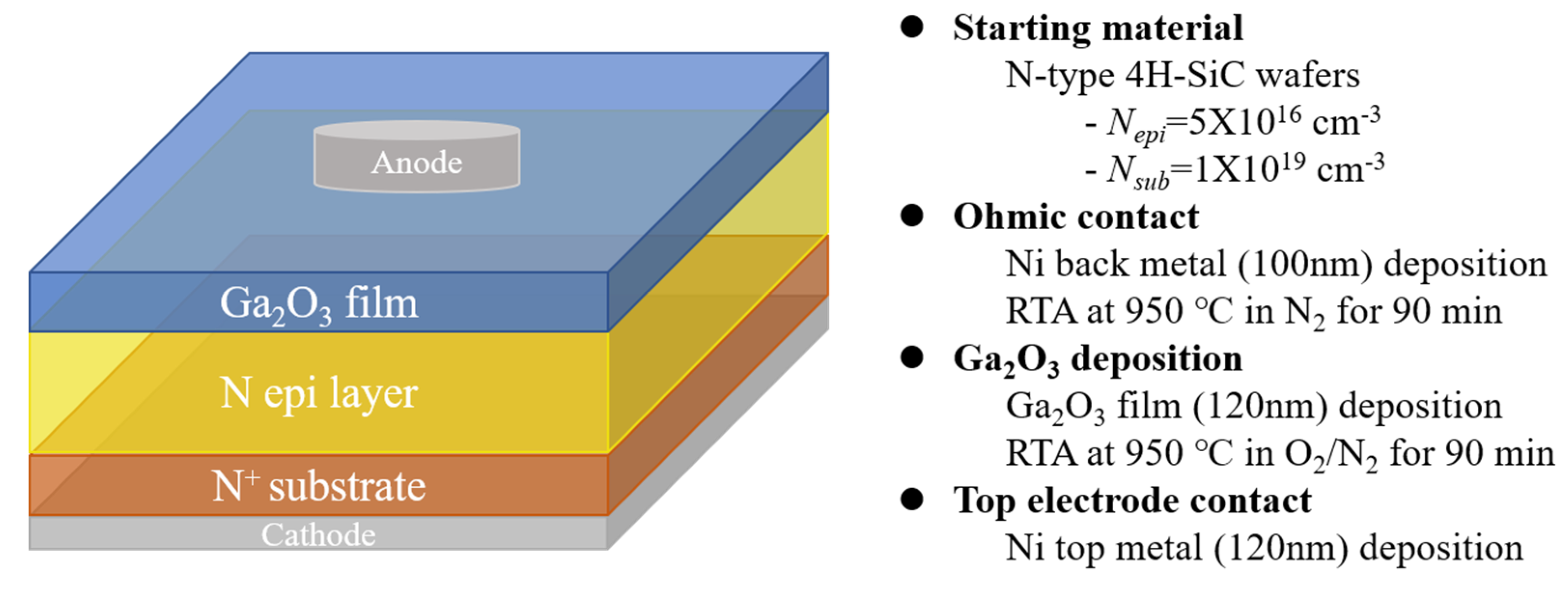
2. Materials and Methods

As a substrate for the gallium oxide film, we used a n-type 4H-SiC wafer (doping concentration: 5 × 1016 cm−3), with a layer of epitaxially grown 4H-SiC (n-type; 1.0 × 1019 cm−3), as shown in Figure 1. After cleaning the SiC wafer with SPM solution (H2SO4:H2O2 = 4:1), we stripped the native silicon dioxide (SiO2) layer using a buffered oxide etch (BOE). A 200-nm-thick nickel film cathode was formed on the bottom side of the SiC wafer by E-beam evaporation. After Ni deposition, the samples were annealed at 950 °C in N2 for 10 min by rapid thermal annealing (RTA) for forming ohmic contacts. Gallium oxide thin films were then deposited by radio frequency (RF) sputtering of a Ga2O3 (99.99% purity) target. Before deposition, the chamber was evacuated to 2.0 × 10⁻⁶ Torr. The films were grown on the epitaxial 4H-SiC layer under 35 mTorr at a pure argon mass flow rate of 4.6 sccm. The RF power was 140 W, and the films were deposited on room temperature. The thickness of the deposited films ranged from 100 to 250 nm. The SiC wafers, with the deposited Ga2O3 films, were annealed at 800 °C for 40 min under different atmospheres (pure oxygen and nitrogen gas). An electrode was formed by deposition of 120 nm of nickel on the Ga2O3 layer.

3. Results

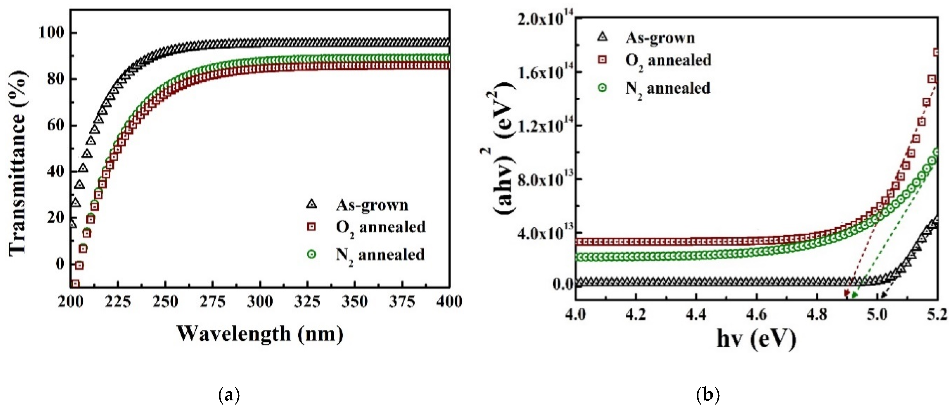
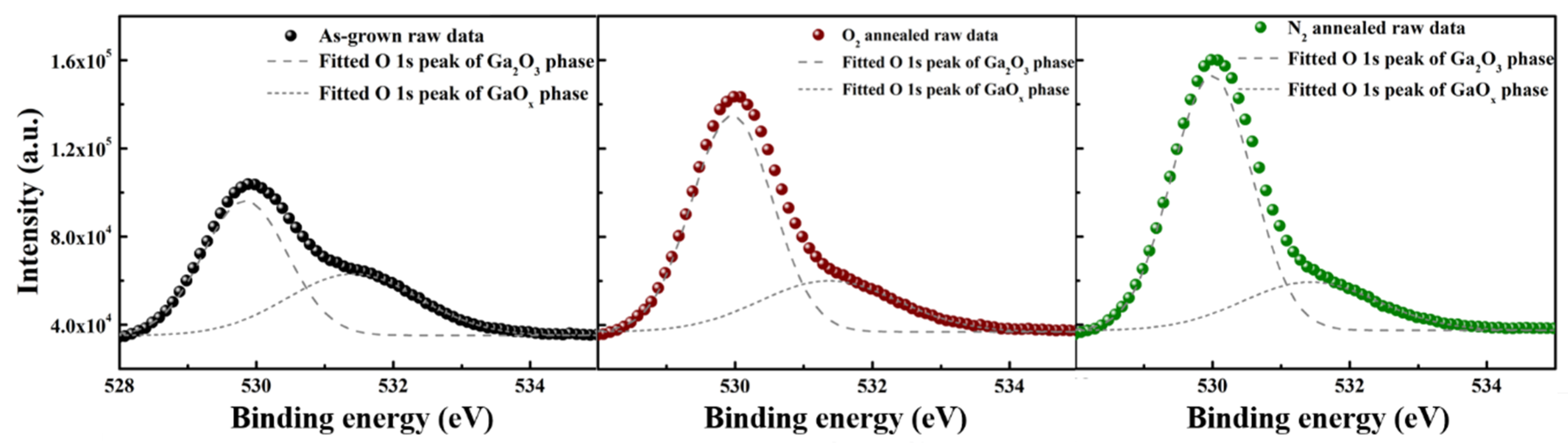
3.1. Material Properties

To compare the influence of different annealing atmospheres on the crystallinity of Ga2O3 deposited on the 4H-SiC substrates, X-ray diffraction (XRD) θ–2θ scans were performed on the as-grown, O2 and N2–annealed samples. As shown in Figure 2, all the sample sets show reflections corresponding to polycrystalline Ga2O3 with a monoclinic structure from Rietveld refinement by using General Structure Analysis System (GSAS) [18,19]. All the manufactured samples give β-Ga2O3 diffraction peaks corresponding to (−201), (−401), and (002) faces. The crystal structures remained stable. In fact, the peak intensities were further enhanced after annealing. In particular, the peak intensities corresponding to the (−201) and (−401) faces significantly increased after N2 annealing. As explained in the literature, Ga and O atoms migrate under high-temperature annealing and thus help improve the crystallinity of Ga2O3. Furthermore, dangling bonds related to oxygen defects at grain boundaries can be passivated by N2 annealing by incorporating nitrogen atoms at gallium or oxygen lattice sites [20,21]. Consequently, the diffraction peak intensities of the N2-annealed samples are higher than those of the other samples, as nitrogen appears to improve the crystal quality of the Ga2O3 [22,23].
Figure 3a shows the optical transmittance spectra of the samples for wavelengths between 200 and 400 nm. All the samples exhibit a high transmittance (over ~80 %) at wavelengths longer than 300 nm. The oxygen concentration in the Ga2O3 crystals will affect the charge states, which in turn will influence such electrical parameters as bandgap and, consequently, the transmittance [24,25]. The optical bandgap is extracted from the linear part of the graph, shown in Figure 3b, for (αhν)2 = 0, where hν is the photon energy, and α is the coefficient of absorption. α = ln(100/T)/d, where T and d is the transmittance and thickness (120 nm) of the Ga2O3 films, respectively. For the as-grown samples, the bandgap of the Ga2O3 film is found to be ~5.01 eV. The bandgaps of the samples annealed under O2 and N2 atmosphere are ~4.91 and ~4.89 eV, respectively. The bandgap of the N2-annealed sample is close to the typically reported bandgap value of ~4.9 eV for β-phase Ga2O3 [26].
Figure 4 shows the XPS spectra of the O 1s peaks of the three different sample sets. The peaks were calibrated using C 1s at 284.6 eV, in which the O 1s peaks were fitted using two Gaussian peaks, corresponding to Ga2O3 and GaOx phases, respectively. After annealing in O2 and N2 atmosphere, the peak intensity of the GaOx phase decreases, whereas that of the Ga2O3 phase increases. The GaOx peak is reported to have a connection with oxygen vacancies [26]. The magnitude of the peak intensity corresponding to the GaOx phase was reduced, from 37.5% for the as-grown sample to 20.3% and 13.6% for the O2 and N2-annealed samples, respectively. This is considered to indicate a decrease in the number of defects, such as oxygen vacancies and oxygen sites. The atomic ratios of O to Ga in the samples are 1.40, 1.43 and 1.42 for as-grown, O2 and N2 annealed Ga2O3. These different stoichiometric ratios indicate that an increased concentration of O2 in the annealing gas can somewhat raise the number of oxygen atoms in the films.

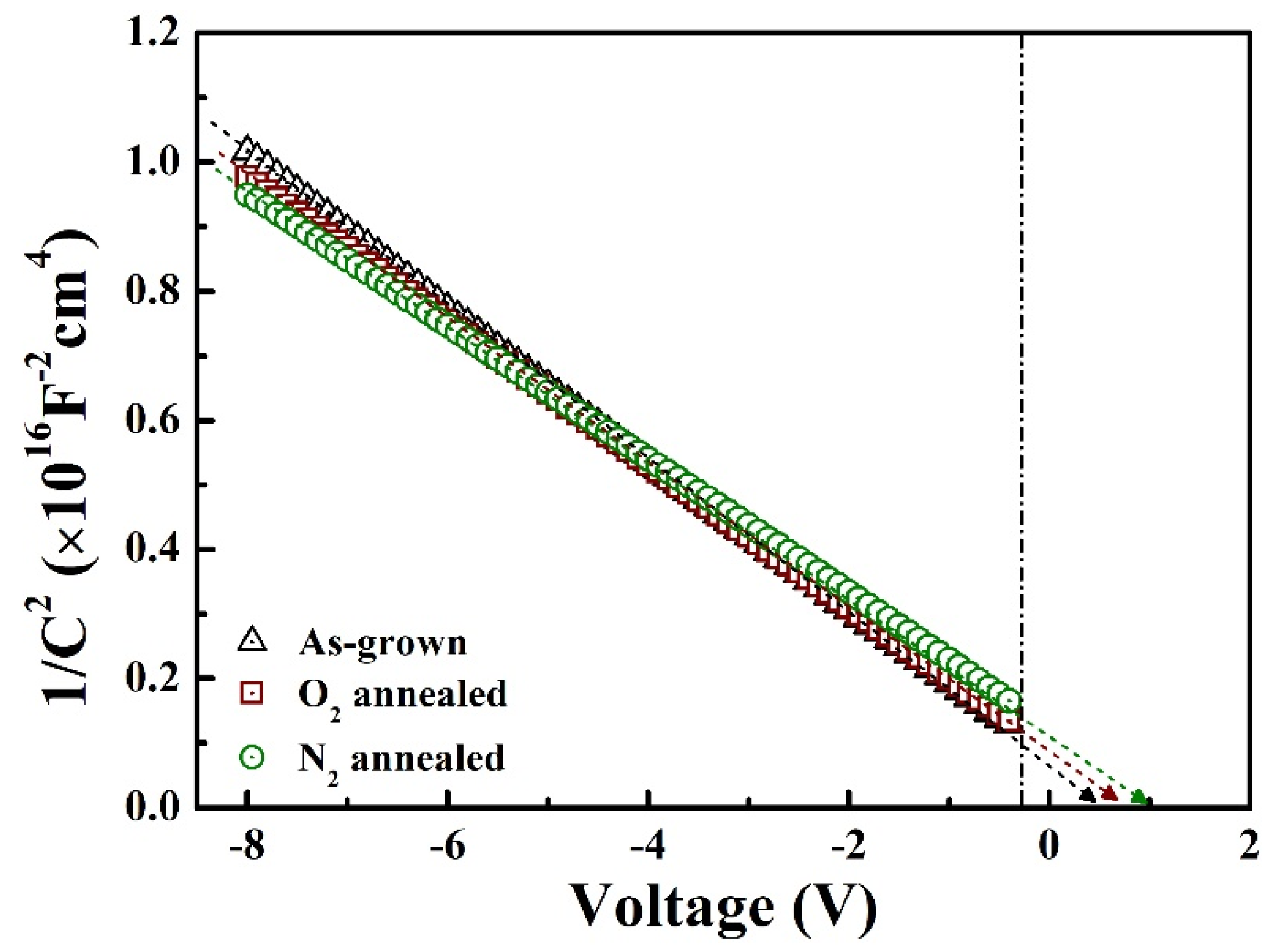
3.2. Electrical Properties

Figure 5 shows the graph of 1/C2 as a function of the reverse voltage bias applied to the Ga2O3/4H-SiC diodes. The built-in voltage (Vbi) and doping concentration can be extracted from the extrapolated graph of 1/C2 versus the voltage. Vbi is calculated from the V-axis intercept of the fitted graph. The doping concentration is derived from the slope of 1/C2–V using Equation (1).
1 C 2 = 2 q A 2 ε G a 2 O 3 N G a 2 O 3 + ε S i C N S i C N G a 2 O 3 N S i C ε G a 2 O 3 ε S i C ( V b i V )
The extracted values of Vbi and doping concentration of the Ga2O3 thin films are 0.47, 0.86, and 1.01 V and 9.59 × 10¹⁵, 1.62 × 10¹⁶, and 2.01 × 1016 cm−3 for the as-grown, O2-annealed, and N2-annealed samples, respectively. The Vbi and doping concentration values increased after annealing, because of the decrease in oxygen-related traps. The increase in the built-in voltage can be attributed to the changes in the dopant concentration and the concentration of interface states of Ga2O3.
Figure 6 shows the typical I–V characteristics of the fabricated Ga2O3/4H-SiC n-n diodes both in the logarithmic and linear scales. As shown in the figure, the as-grown diode has a high leakage current (~1.60 × 10⁻⁵ A) and a low rectifying ratio (~3.0 × 10³) measured at forward (3 V) and reverse biases (−3 V). The rectifying behavior of the O2 and N2-annealed diodes is improved. The different samples exhibit a similar leakage current value of approximately 8.1 × 10⁻¹¹ A. The N2-annealed diode exhibits a higher on-current when a forward voltage is applied, with a rectifying ratio of ~5.0 × 10⁷, which may be related to the reduced oxygen trap concentrations after annealing. The threshold voltages of the diodes are ~1.55, ~1.47, and ~1.27 V for the as-grown, O2 and N2-annealed samples, respectively. The ideality factor at room temperature can be extracted from Equation (2).
I = I O [ e V η K B T 1 ]
Here, I and V are the forward current and voltage, respectively, I0 is the saturation current, kB is Boltzmann’s constant, T is the absolute temperature, and η is the ideality factor. The ideality factor is significantly reduced after the annealing process; the ideality factor of the N2-annealed diode is 2.8, which is half that of the O2-annealed diode. The lower ideality factor and the higher built-in voltage of the annealed diodes are attributed to the improved crystallinity and interface properties.
The thermal activation energy (EA) is obtained from the ln (IO)–1/kT plot shown in Figure 7. The graph was plotted in the temperature range of 298–523 K with a temperature step of 25 K, where IO is the reverse saturation current at −3 V, and T and k are the absolute temperature and Boltzmann’s constant, respectively. The extracted activation energy from the experimental measurements are related to trap states at the metal–Ga2O3 interfaces and the barrier heights. Low activation energy values suggest a high concentration of the trap states at the interface, which results in increased trap-assisted tunneling or thermionic emission probabilities across the barrier. As shown in Figure 6, the extracted activation energy of the devices increases after annealing. In particular, the activation energy of the N2-annealed sample (0.504 eV) is twice that of the as-grown sample. The improved rectifying ratio of the N2-annealed diode is also attributed to the increased activation energy.

4. Conclusions

We fabricated polycrystalline β-Ga2O3/4H-SiC heterojunction diodes annealed under different gas atmospheres (O2 and N2). The material and electrical properties of the diodes were investigated to understand the effects of the different annealing gases on the device characteristics. X-ray diffraction peaks corresponding to the different faces of β-Ga2O3 {(−201), (−402), and (002)} were observed to significantly increase, while the bandgap somewhat decreased to ~4.9 eV after annealing. The post-annealing decrease in the GaOx peak intensity indicates a decrease in the number of oxygen vacancies. With regard to the electrical properties, the leakage current decreased nearly 1000 times after annealing. To summarize, the N2-annealed sample exhibited higher rectifying ratio and built in voltage, decreased threshold voltage, lower ideality factor, and higher activation energy than the as-grown and O2-annealed samples. Therefore, we conclude that the performance of N2-annealed diodes at high temperatures is more stable due to higher activation energy compare with built-in voltage due to a lower concentration of trap states.

Author Contributions

Supervision and conceptualization, S.-M.K.; formal analysis and writing—original draft preparation, Y.-J.L.; writing, M.A.S.; visualization, J.-M.O. All authors have read and agreed to the published version of the manuscript.

Funding

This work was supported by the NRF (2018R1D1A1B07047515) and Korea Electric Power Corporation (R17XA05-60).

Conflicts of Interest

The authors declare no conflicts of interest.

References

  1. Oshima, T.; Okuno, T.; Arai, N.; Suzuki, N.; Ohira, S.; Fujita, S. Vertical Solar-Blind Deep-Ultraviolet Schottky Photodetectors Based on β-Ga2O3 Substrates. Appl. Phys. Express 2008, 1, 011202. [Google Scholar] [CrossRef]
  2. Feng, Z.; Huang, L.; Feng, Q.; Li, X.; Zhang, H.; Tang, W.; Zhang, J.; Hao, Y. MOCVD grown β-Ga2O3 metal-oxide-semiconductor field effect transistors on sapphire. Appl. Phys. Express 2018, 8, 8. [Google Scholar]
  3. An, Y.H.; Guo, D.Y.; Li, S.Y.; Wu, Z.P.; Huang, Y.Q.; Li, P.G.; Li, L.H.; Tang, W.H. Influence of oxygen vacancies on the photoresponse of β-Ga2O3 /SiC n–n type heterojunctions. J. Phys. D Appl. Phys. 2016, 49, 285111. [Google Scholar] [CrossRef]
  4. Guo, Y.; Li, A.; Feng, Q.; Hu, Z.; Feng, Z.; Zhang, K.; Lu, X.; Zhang, C.; Zhou, H.; Mu, W.; et al. High-Voltage β-Ga2O3 Schottky Diode with Argon-Implanted Edge Termination. Nanoscale Res. Lett. 2019, 14, 8. [Google Scholar] [CrossRef] [PubMed] [Green Version]
  5. Yang, J.; Sparks, Z.; Ren, F.; Pearton, S.J.; Tadjer, M. Effect of surface treatments on electrical properties of β-Ga2O3. J. Vac. Sci. Technol. B 2018, 36, 061201. [Google Scholar] [CrossRef]
  6. Dong, L.; Jia, R.; Xin, B.; Zhang, Y. Effects of post-annealing temperature and oxygen concentration during sputtering on the structural and optical properties of β-Ga2O3 films. J. Vac. Sci. Technol. A Vac. Surf. Films 2016, 34, 060602. [Google Scholar] [CrossRef]
  7. Zhang, H.; Deng, J.; Pan, Z.; Bai, Z.; Kong, L.; Wang, J. Structural and optical properties of Nb-doped β-Ga2O3 thin films deposited by RF magnetron sputtering. Vacuum 2017, 146, 93–96. [Google Scholar] [CrossRef]
  8. Zhang, Y.; Yan, J.; Li, Q.; Qu, C.; Zhang, L.; Xie, W. Optical and structural properties of Cu-doped β-Ga2O3 films. Mater. Sci. Eng. B 2011, 176, 846–849. [Google Scholar] [CrossRef]
  9. Takeuchi, T.; Ishikawa, H.; Takeuchi, N.; Horikoshi, Y. High resolution X-ray photoelectron spectroscopy of beta gallium oxide films deposited by ultra high vacuum radio frequency magnetron sputtering. Thin. Solid Films 2008, 516, 4593–4597. [Google Scholar] [CrossRef]
  10. Ishibashi, K.; Aida, R.; Takahara, M.; Kudo, J.; Tsunoda, I.; Takakura, K.; Nakashima, T.; Shibuya, M.; Murakami, K. Investigation of the crystalline quality of a gallium oxide thick film grown by RF magnetron sputtering. Phys. Status Solidi 2013, 10, 1588–1591. [Google Scholar]
  11. Donmez, I.; Akgun, C.O.; Biyikli, N. Fabrication of AlN/BN bishell hollow nanofibers by electrospinning and atomic layer deposition. J. Vac. Sci. Technol. A 2014, 32, 4. [Google Scholar]
  12. Battu, A.K.; Ramana, C.V. Mechanical Properties of Nanocrystalline and Amorphous Gallium Oxide Thin Films. Adv. Eng. Mater. 2018, 20, 1701033. [Google Scholar] [CrossRef]
  13. Varley, J.; Weber, J.R.; Janotti, A.; van de Walle, C.G. Oxygen vacancies and donor impurities in β-Ga2O3. Appl. Phys. Lett. 2018, GAO2018, 142106. [Google Scholar] [CrossRef]
  14. Rebien, M.; Henrion, W.; Hong, M.; Mannaerts, J.P.; Fleischer, M. Optical properties of gallium oxide thin films. Appl. Phys. Lett. 2002, 81, 250. [Google Scholar] [CrossRef] [Green Version]
  15. Ghose, S. Structural and optical properties of β-Ga2O3 thin films grown by plasma-assisted molecular beam epitaxy. J. Vac. Sci. Technol. B Nanotechnol. Microelectron. Mater. Process. Meas. Phenom. 2016, 34, 02L109. [Google Scholar] [CrossRef]
  16. Kang, H.C. Heteroepitaxial growth of multidomain Ga2O3/sapphire(001) thin films deposited using radio frequency magnetron sputtering. Mater. Lett. 2014, 119, 123–126. [Google Scholar] [CrossRef]
  17. Nakagomi, S.; Sakai, T.; Kikuchi, K.; Kokubun, Y. β-Ga2O3/p-Type 4H-SiC Heterojunction Diodes and Applications to Deep-UV Photodiodes. Phys. Status Solidi. A 2018, 216, 1700796. [Google Scholar] [CrossRef]
  18. Trukhanov, S.V.; Trukhanov, A.V.; Panina, L.V.; Kostishyn, V.G.; Turchenko, V.A.; Trukhanova, E.L.; Trukhanov, A.V.; Zubar, T.I.; Ivanov, V.M.; Tishkevich, D.I.; et al. Temperature evolution of the structure parameters and exchange interactions in BaFe12−xInxO19. J. Magn. Magn. Mater. 2018, 466, 393–405. [Google Scholar] [CrossRef]
  19. Pashchenko, A.V.; Liedienov, N.A.; Li, Q.; Tatarchuk, D.D.; Turchenko, V.A.; Makoed, I.I.; Sycheva., V.Y.; Voznyak, A.V.; Kladko, V.P.; Gudimenko, A.I.; et al. Structure, non-stoichiometry, valence of ions, dielectric and magnetic properties of single-phase Bi0.9La0.1FeO3−δ multiferroics. J. Magn. Magn Mater. 2019, 483, 100–113. [Google Scholar] [CrossRef]
  20. Zhang, Z.; Farzana., E.; Arehart., A.R.; Ringel, S.A. Deep level defects throughout the bandgap of (010) β-Ga2O3 detected by optically and thermally stimulated defect spectroscopy. Appl. Phys. Lett. 2016, 108, 052105. [Google Scholar] [CrossRef]
  21. Rafique, S.; Han, L.; Zhao, H. Thermal annealing effect on β-Ga2O3 thin film solar blind photodetector heteroepitaxially grown on sapphire substrate. Phys. Status Solidi. A. 2017, 214, 8. [Google Scholar] [CrossRef]
  22. Wang, J.; Ye, L.; Wang, X.; Zhang, H.; Li, L.; Kong, C.; Li, W. High transmittance β-Ga2O3 thin films deposited by magnetron sputtering and post-annealing for solar-blind ultraviolet photodetector. J. Alloys Compd. 2019, 803, 9–15. [Google Scholar] [CrossRef]
  23. Sun, R.; Zhang, H.Y.; Wang, G.G.; Han, J.C.; Wang, X.Z.; Kuang, X.P.; Cui, L.; Jin, L.; Tia, J.L. Influence of annealing atmosphere on the structure, morphology and transmittance of N-incorporated Ga2O3 films. Superlattices Microstruct. 2013, 60, 257–262. [Google Scholar] [CrossRef]
  24. Trukhanov, S.V.; Lobanovski, L.S.; Bushinsky, M.V.; Khomchenko, V.A.; Pushkarev, N.V.; Troyanchuk, I.O.; Maignan, A.; Flahaut, D.; Szymczak, H.; Szymczak, R. Influence of oxygen vacancies on the magnetic and electrical properties of La1−xSrxMnO3−x/2 manganites. Eur. Phys. J. B – Condens. Matter Complex Syst. 2004, 42, 51–61. [Google Scholar] [CrossRef]
  25. Shang, C.; Xia, Z.C.; Zhai, X.A.; Liu, D.W.; Wang, Y.Q. Percolation like transitions in phase separated manganites La0.5Ca0.5Mn1−xAlxO3−δ. Ceram. Int. 2019, 45, 18632–18639. [Google Scholar] [CrossRef]
  26. Higashiwaki, M.; Sasaki, K.; Murakami, H.; Kumagai, Y.; Koukitu, A.; Kuramata, A.; Masui, T.; Yamakoshi, S. Recent progress in Ga2O3 power devices. Semicond. Sci. Technol. 2016, 31, 034001. [Google Scholar] [CrossRef]
Figure 1. Structure of Ga2O3/4H-SiC heterojunction diode and fabrication flow.
Materials 13 00434 g001
Figure 2. XRD spectra of samples and refinement results of Ga2O3 annealed under different atmosphere.
Materials 13 00434 g002
Figure 3. (a) Transmittance spectra and (b) (αhν)2–hν plots of Ga2O3 film samples annealed under different atmospheres.
Materials 13 00434 g003
Figure 4. O 1s XPS spectra of the Ga2O3 films annealed under different atmospheres.
Materials 13 00434 g004
Figure 5. 1/C2–reverse voltage plots for different diodes measured at room temperature.
Materials 13 00434 g005
Figure 6. I–V characteristics of diodes at room temperature: (a) log-scale and (b) linear curves.
Materials 13 00434 g006
Figure 7. ln(IO)–1/kT curve for activation energy values derived from the increasing temperature.
Materials 13 00434 g007

