Surface Characterization of MoS2 Atomic Layers Mechanically Exfoliated on a Si Substrate


Abstract
1. Introduction
2. Experimental
3. Results and Discussion
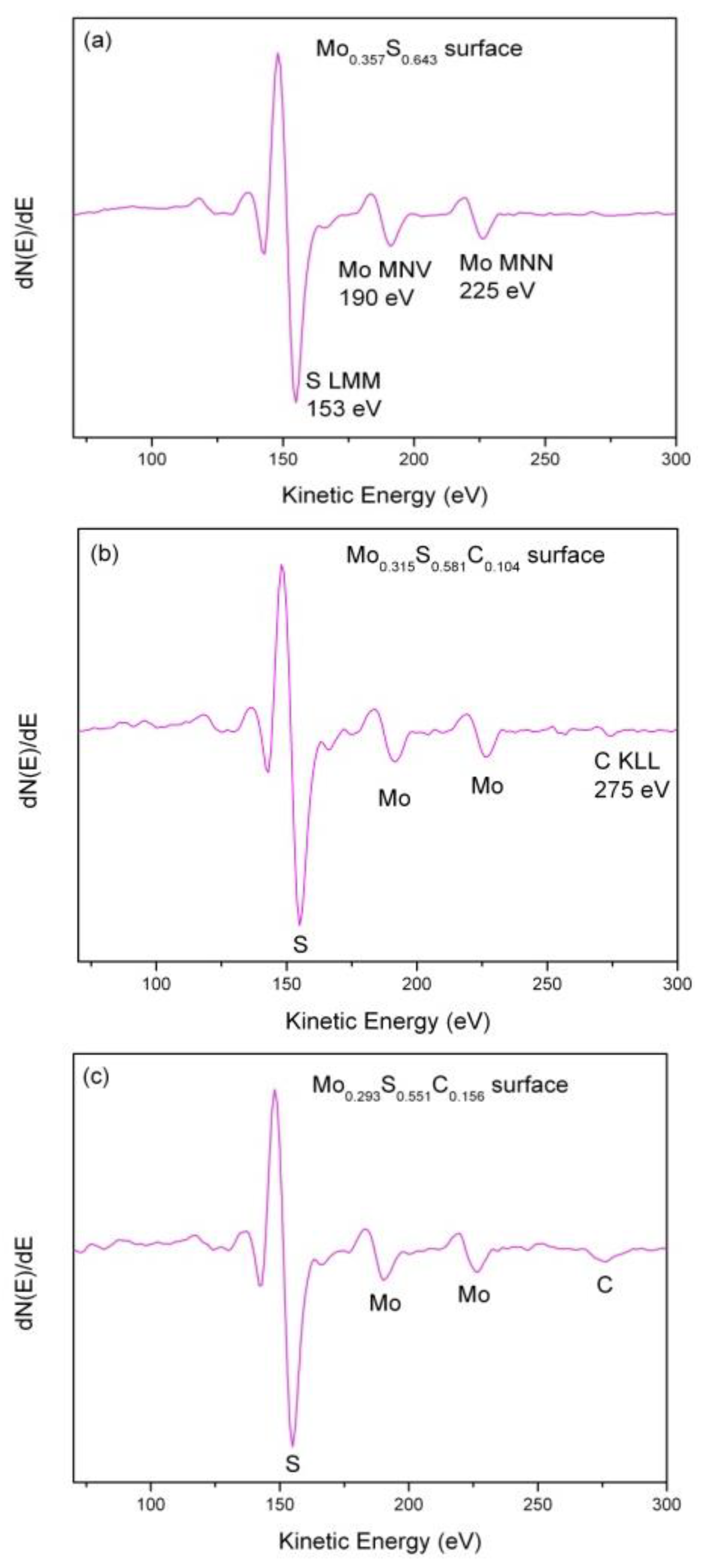
3.1. Auger Electron Spectroscopy (AES) Characterization
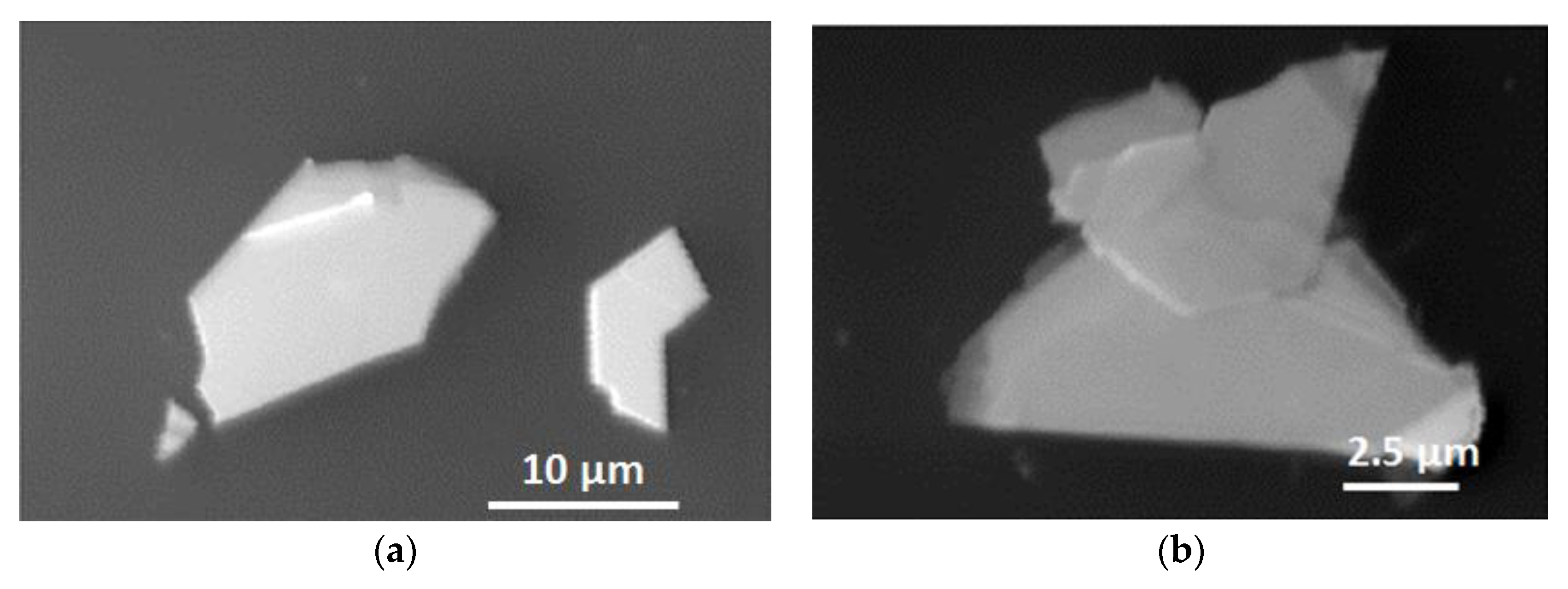
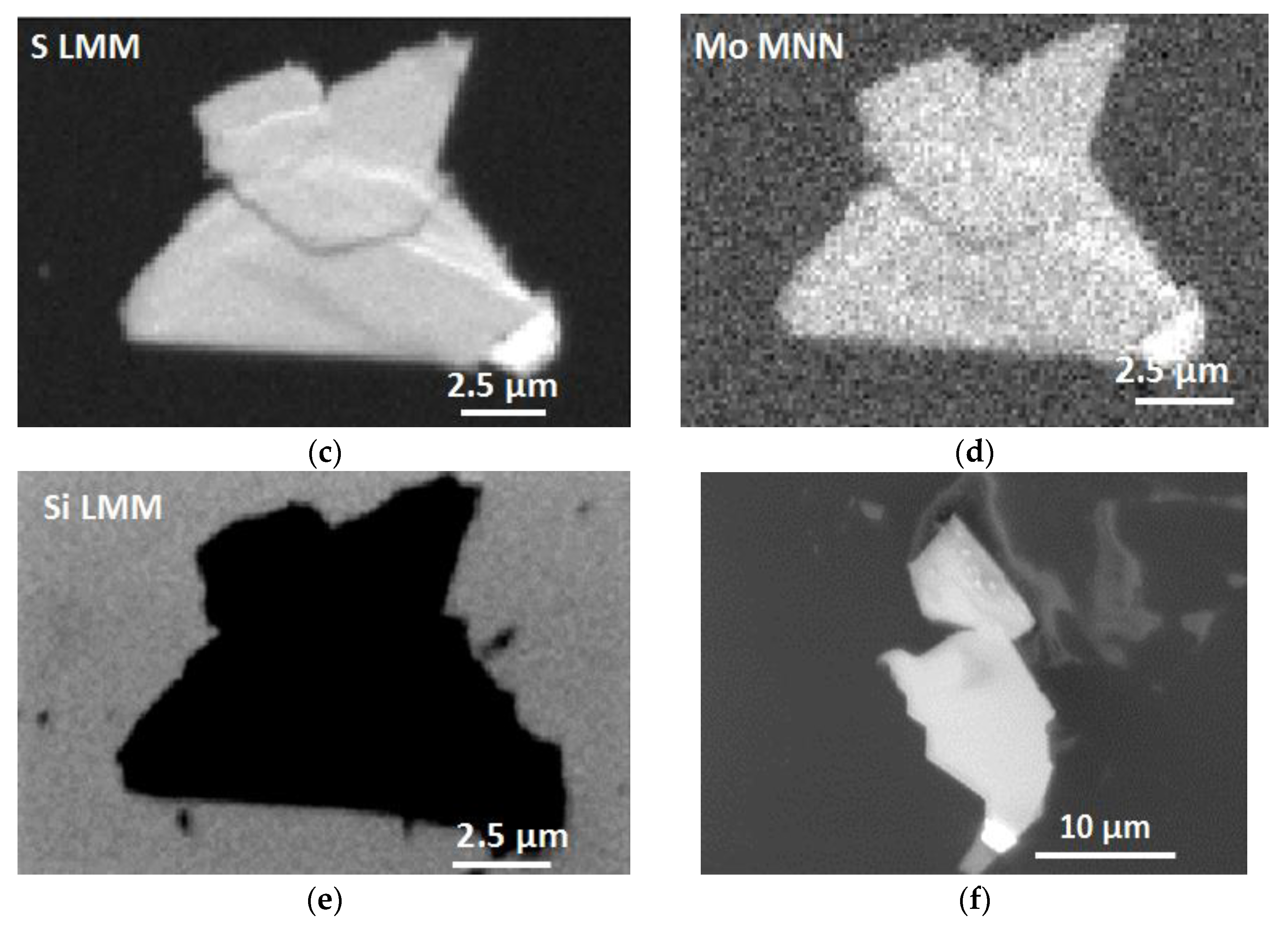
3.2. Scanning Electron Microscopy (SEM) Characterization
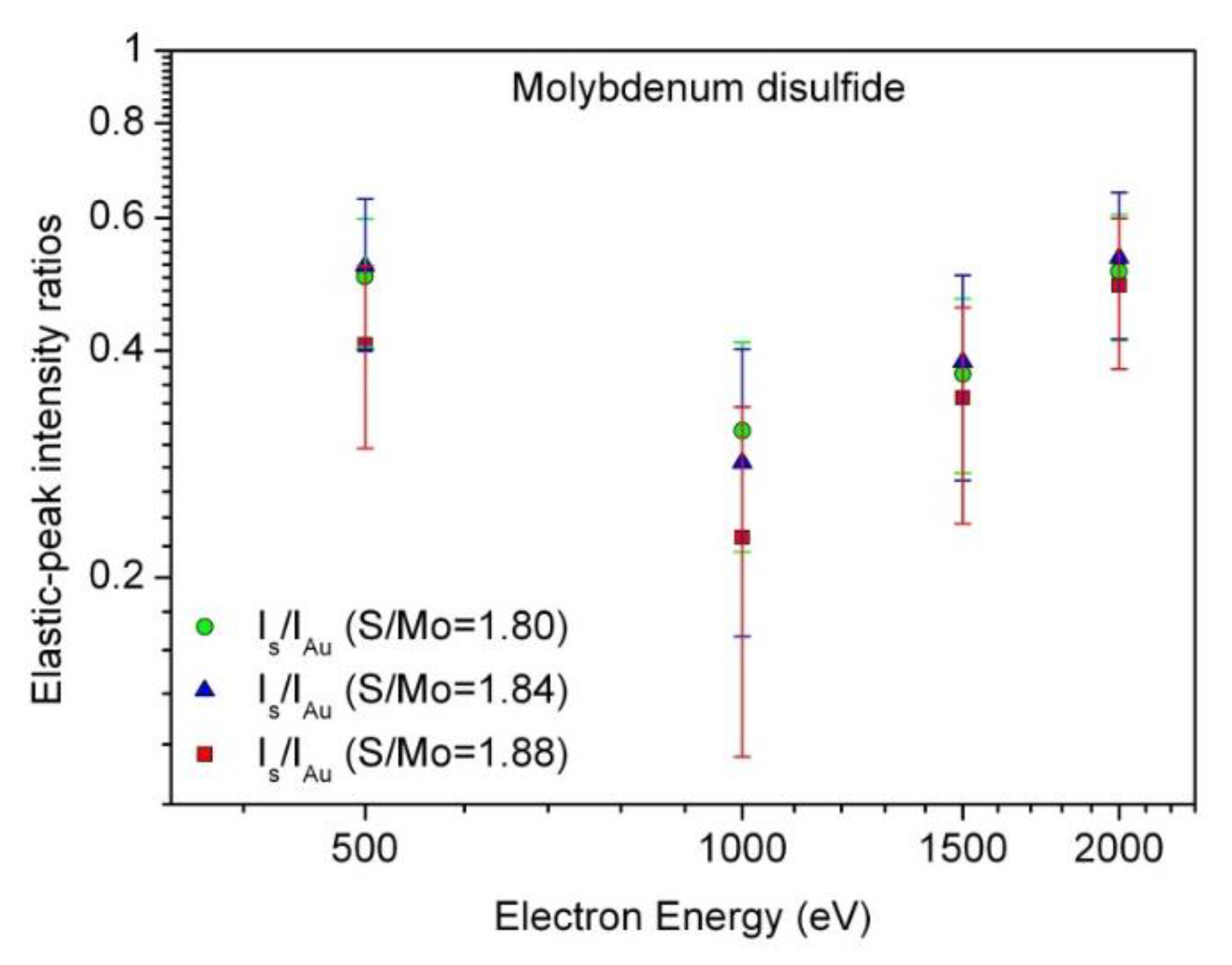
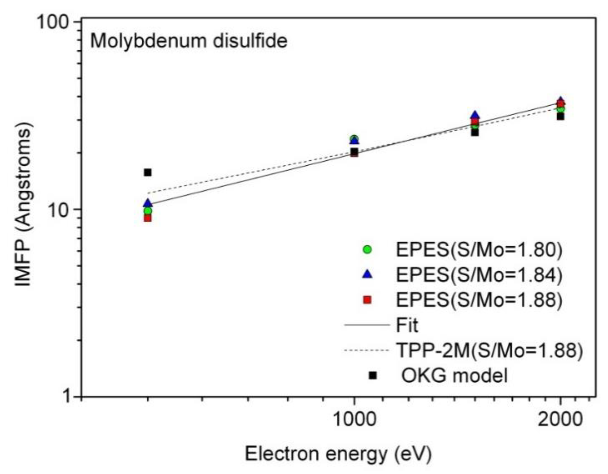
3.3. Elastic-Peak Electron Spectroscopy (EPES) Characterization: Evaluation of the Electron Inelastic Mean Free Path (IMFP)
4. Conclusions
Author Contributions
Funding
Conflicts of Interest
References
- Huang, X.; Zeng, Z.; Zhang, H. Metal dichalcogenide nanosheets: Preparation, properties and applications. Chem. Soc. Rev. 2013, 42, 1934–1946. [Google Scholar] [CrossRef]
- Wang, Q.H.; Kalantar-Zadeh, K.; Kis, A.; Coleman, J.N.; Strano, M.S. Electronics and optoelectronics of two-dimensional transition metal dichalcogenides. Nat. Nanotechnol. 2012, 7, 699–712. [Google Scholar]
- Feng, J.; Qian, X.; Huang, C.; Li, J. Strain-engineered artificial atom as a broad-spectrum solar energy funnel. Nat. Photonics 2012, 6, 866–872. [Google Scholar] [CrossRef]
- Mak, K.F.; McGill, K.L.; Park, J.; McEuen, P.L. The valley Hall effect in MoS2 transistors. Science 2014, 344, 1489–1492. [Google Scholar] [CrossRef] [PubMed]
- Karunadasa, H.I.; Montalvo, E.; Sun, Y.; Majda, M.; Long, J.R.; Chang, C.J. A molecular MoS2 edge site mimic for catalytic hydrogen generation. Science 2012, 335, 698–702. [Google Scholar] [CrossRef] [PubMed]
- Lukowski, M.A.; Daniel, A.S.; Meng, F.; Forticaux, A.; Li, L.; Jin, S. Enhanced hydrogen evolution catalysis from chemically exfoliated metallic MoS2 nanosheets. J. Am. Chem. Soc. 2013, 135, 10274–10277. [Google Scholar] [CrossRef] [PubMed]
- Xie, J.; Zhang, H.; Li, S.; Wang, R.; Sun, X.; Zhou, M.; Zhou, J.; Lou, X.W.; Xie, Y. Defect-rich MoS2 ultrathin nanosheets with additional active edge sites for enhanced electrocatalytic hydrogen evolution. Adv. Mater. 2013, 25, 5807–5813. [Google Scholar] [CrossRef] [PubMed]
- Kim, S.-Y.; Kwak, J.; Ciobanu, C.V.; Kwon, S.-Y. Recent developments in controlled vapor-phase growth of 2D group 6 transition metal dichalcogenides. Adv. Mater. 2019, 31, 1804939. [Google Scholar] [CrossRef]
- Kalanyan, B.; Beams, R.; Katz, M.B.; Davydov, A.V.; Maslar, J.E.; Kanjolia, R.K. MoS2.thin films from a (Nt Bu)2 (NMe2)2 Mo and 1-propanethiol atomic layer deposition process. J. Vac. Sci. Technol. 2019, 37. [Google Scholar] [CrossRef]
- Powell, C.J.; Jablonski, A. Evaluation of calculated and measured electron inelastic mean free paths near solid surfaces. J. Phys. Chem. Ref. Data 1999, 28, 19–62. [Google Scholar] [CrossRef]
- Penn, D.R. Electron mean-free-path calculations using a model dielectric function. Phys. Rev. 1987, B 35, 482–486. [Google Scholar] [CrossRef]
- Tanuma, S.; Powell, C.J.; Penn, D.R. Calculations of electron inelastic mean free paths: VIII. Data for 15 elemental solids over the 50–2000 eV range. Surf. Interface Anal. 2005, 37, 1–14. [Google Scholar] [CrossRef]
- Tanuma, S.; Powell, C.J.; Penn, D.R. Calculation of electron inelastic mean free paths. (IMFPs) VII. Reliability of the TPP-2M IMFP predictive equation. Surf. Interface Anal. 2003, 35, 268–275. [Google Scholar] [CrossRef]
- Tanuma, S.; Powell, C.J.; Penn, D.R. Calculations of electron inelastic mean free paths. IX. Data for 41 elemental solids over the 50 eV to 30 keV range. Surf. Interface Anal. 2011, 43, 689–713. [Google Scholar] [CrossRef]
- Gergely, G. Elastic peak electron spectroscopy for auger electron spectroscopy and electron energy loss spectroscopy. Surf. Interface Anal. 1981, 3, 201–205. [Google Scholar] [CrossRef]
- Jablonski, A. Determination of the electron inelastic mean free path in solids from the elastic electron backscattering intensity. Surf. Interface Anal. 2005, 37, 1035–1044. [Google Scholar] [CrossRef]
- Jablonski, A. Surface sensitivity of elastic peak electron spectroscopy. Appl. Surf. Sci. 2016, 378, 87–101. [Google Scholar] [CrossRef]
- Krawczyk, M.; Lisowski, W.; Pisarek, M.; Nikiforow, K.; Jablonski, A. Surface characterization of low-temperature grown yttrium oxide. Appl. Surf. Sci. 2018, 437, 347–356. [Google Scholar] [CrossRef]
- Tanuma, S.; Powell, C.J.; Penn, D.R. Calculations of electron inelastic mean free paths. V. Data for 14 organic compounds over the 50–2000 eV range. Surf. Interface Anal. 1994, 21, 165–176. [Google Scholar] [CrossRef]
- Dubus, A.; Jablonski, A.; Tougaard, S. Evaluation of theoretical models for elastic electron backscattering from surfaces. Progress Surf. Sci. 2000, 63, 135–175. [Google Scholar] [CrossRef]
- Oswald, R.; Kasper, E.; Gaukler, K.H. A multiple scattering theory of elastic electron backscattering from amorphous surfaces. J. Electr. Spectrosc. Relat. Phenom. 1993, 61, 251–274. [Google Scholar] [CrossRef]
- Jablonski, A. Determination of the IMFP from electron elastic backscattering probability. Surf. Interface Anal. 2000, 29, 582–595. [Google Scholar] [CrossRef]
- Jablonski, A. Angular distribution of elastic electron backscattering from surfaces: Determination of the electron inelastic mean free path. J. Phys. D Appl. Phys. 2014, 47, 055301. [Google Scholar] [CrossRef]
- Jablonski, A. Analytical theory of elastic electron backscattering from elements, alloys, and compounds: Comparison with experimental data. J. Electr. Spectr. Rel. Phenom. 2016, 206, 24–45. [Google Scholar] [CrossRef]
- Yi, M.; Shen, Z. A review on mechanical exfoliation for the scalable production of graphene. J. Mater. Chem. 2015, 3, 11700–11715. [Google Scholar] [CrossRef]
- Spychalski, W.L.; Pisarek, M.; Szoszkiewicz, R. Microscale insight into oxidation of single MoS2 crystals in air. J. Phys. Chem. 2017, 121, 26027–26033. [Google Scholar] [CrossRef]
- Ukegbu, U.; Szoszkiewicz, R. Microscopic kinetics of heat-induced oxidative etching of thick MoS2 crystals. J. Phys. Chem. 2019, 123, 22123–22129. [Google Scholar] [CrossRef]
- Childs, K.D.; Carlson, B.A.; LaVanier, L.A.; Moulder, J.F.; Paul, D.F.; Stickle, W.F.; Watson, D.G. Handbook of Auger Electron Spectroscopy, a Book of Reference Data for Identification and Interpretation in Auger Electron Spectroscopy, 3rd ed.; Hedberg, C.L., Ed.; Physical Electronics Inc.: Eden Prairie, MN, USA, 1995. [Google Scholar]
- Jablonski, A.; Zemek, J. Remarks on some reference materials for applications in elastic peak electron spectroscopy. Anal. Sci. 2010, 26, 239–246. [Google Scholar] [CrossRef][Green Version]
- Jablonski, A.; Krawczyk, M. Determination of the Electron IMFP from Elastic Peak Electron Spectroscopy, Users’ Guide, 1st ed.; Institute of Physical Chemistry, Polish Academy of Sciences: Warsaw, Poland, 2014; (Electronic version obtainable from authors). [Google Scholar]
- Wang, X.; Cormier, C.R.; Khosravi, A.; Smyth, C.M.; Shallenberger, J.R.; Addou, R.; Wallace, R.M. In situ exfoliated 2D molybdenum disulfide analyzed by XPS. Surf. Sci. Spectra 2020, 27. [Google Scholar] [CrossRef]
- Powell, C.J.; Jablonski, A. NIST Electron. Inelastic-Mean-Free-Path Database SRD 71: Version 1.2; National Institute of Standards and Technology: Gaithersburg, MA, USA, 2010. [Google Scholar]
- Ataca, C.; Sahin, H.; Ciraci, S. Stable, single-layer MX2 transition-metal oxides and dichalcogenides in a honeycomb-like structure. J. Phys. Chem. 2012, C 116, 8983–8999. [Google Scholar] [CrossRef]
- Mak, K.F.; Lee, C.; Hone, J.; Shan, J.; Heinz, T.F. Atomically thin MoS2: A new direct-.gap semiconductor. Phys. Rev. Lett. 2010, 105, 136805. [Google Scholar] [CrossRef]
- Haynes, W.M. CRC Handbook of Chemistry and Physics, 94th ed.; CRC Press: Boca Raton, FL, USA; New York, NY, USA; London, UK, 2013. [Google Scholar]
- Szoszkiewicz, R.; Rogala, M.; Dąbrowski, P. Surface-bound and volatile Mo oxides produced during oxidation of single MoS2 crystals in air and high relative humidity. Materials 2020, 13, 3067. [Google Scholar] [CrossRef]


| IMFP (nm) | ||||||
|---|---|---|---|---|---|---|
| Surface Stoichiometry (in S/Mo AC Ratios) | ||||||
| S/Mo = 1.80 | S/Mo = 1.84 | S/Mo = 1.88 | S/Mo = 1.88 | S/Mo = 2.00 | ||
| E (eV) | EPES | EPES | EPES | TPP-2M | OKG theory | TPP-2M |
| 500 | 0.98 | 1.07 | 0.90 | 1.22 | 1.57 | 1.19 |
| 1000 | 2.37 | 2.31 | 1.99 | 2.03 | 2.03 | 1.98 |
| 1500 | 2.81 | 3.16 | 2.93 | 2.77 | 2.57 | 2.70 |
| 2000 | 3.45 | 3.75 | 3.66 | 3.48 | 3.13 | 3.39 |
| Δj Deviation (%) | ||||
|---|---|---|---|---|
| Energy(eV) | S/Mo = 1.80 | S/Mo = 1.84 | S/Mo = 1.88 | Δf Deviation (%) |
| 500 | −4.85 | 3.88 | −12.62 | −13.44 |
| 1000 | 19.09 | 16.08 | 0 | 0.50 |
| 1500 | −3.77 | 8.22 | 0.34 | 8.15 |
| 2000 | −9.92 | −2.09 | −4.44 | 12.98 |
© 2020 by the authors. Licensee MDPI, Basel, Switzerland. This article is an open access article distributed under the terms and conditions of the Creative Commons Attribution (CC BY) license (http://creativecommons.org/licenses/by/4.0/).
Share and Cite
Krawczyk, M.; Pisarek, M.; Szoszkiewicz, R.; Jablonski, A. Surface Characterization of MoS2 Atomic Layers Mechanically Exfoliated on a Si Substrate. Materials 2020, 13, 3595. https://doi.org/10.3390/ma13163595
Krawczyk M, Pisarek M, Szoszkiewicz R, Jablonski A. Surface Characterization of MoS2 Atomic Layers Mechanically Exfoliated on a Si Substrate. Materials. 2020; 13(16):3595. https://doi.org/10.3390/ma13163595
Chicago/Turabian StyleKrawczyk, Mirosław, Marcin Pisarek, Robert Szoszkiewicz, and Aleksander Jablonski. 2020. "Surface Characterization of MoS2 Atomic Layers Mechanically Exfoliated on a Si Substrate" Materials 13, no. 16: 3595. https://doi.org/10.3390/ma13163595
APA StyleKrawczyk, M., Pisarek, M., Szoszkiewicz, R., & Jablonski, A. (2020). Surface Characterization of MoS2 Atomic Layers Mechanically Exfoliated on a Si Substrate. Materials, 13(16), 3595. https://doi.org/10.3390/ma13163595