Article

AlxIn1−xN on Si (100) Solar Cells (x = 0–0.56) Deposited by RF Sputtering

1
Photonics Engineering Group, University of Alcalá, 28871 Alcalá de Henares, Spain
2
Thin Film and Microelectronics Group, University Complutense of Madrid, 28040 Madrid, Spain
3
Electronics and Semiconductors Group, Applied Physics Department, Universidad Autónoma de Madrid, 28049 Madrid, Spain
*
Author to whom correspondence should be addressed.
Materials 2020, 13(10), 2336; https://doi.org/10.3390/ma13102336
Submission received: 17 April 2020 / Revised: 11 May 2020 / Accepted: 13 May 2020 / Published: 19 May 2020
(This article belongs to the Special Issue Advanced Materials for Photonics and Photovoltaics Applications)

Abstract

:
We investigate the photovoltaic performance of solar cells based on n-AlxIn1−xN (x = 0–0.56) on p-Si (100) hetero-junctions deposited by radio frequency sputtering. The AlxIn1−xN layers own an optical bandgap absorption edge tuneable from 1.73 eV to 2.56 eV within the Al content range. This increase of Al content results in more resistive layers (≈10−4–1 Ω·cm) while the residual carrier concentration drops from ~1021 to ~1019 cm−3. As a result, the top n-contact resistance varies from ≈10−1 to 1 MΩ for InN to Al0.56In0.44N-based devices, respectively. Best results are obtained for devices with 28% Al that exhibit a broad external quantum efficiency covering the full solar spectrum with a maximum of 80% at 750 nm, an open-circuit voltage of 0.39 V, a short-circuit current density of 17.1 mA/cm2 and a conversion efficiency of 2.12% under air mass 1.5 global (AM1.5G) illumination (1 sun), rendering them promising for novel low-cost III-nitride on Si photovoltaic devices. For Al contents above 28%, the electrical performance of the structures lessens due to the high top-contact resistivity.

1. Introduction

Nowadays, the main goal of the photovoltaic industry is to develop novel technologies that manage to simultaneously improve device efficiency and reduce fabrication costs. In that sense, materials such as perovskites [1] and III-V compounds [2] have obtained great results. However, new low-cost materials are needed to complement the already established Si technology. III-nitride semiconductors and alloys are very promising for application in solar cells because of their tunable wide direct bandgap energy from the near-infrared (0.7 eV, InN) to the ultraviolet (6.2 eV, AlN) and their particular material properties, such as thermal and chemical stability, make them quite promising to be used in space applications [3].
The difficulties of growing high-quality and single-phase AlxIn1−xN relies on the big differences between its binary constituents, InN and AlN (bonding energies, lattice mismatch, and growth temperature) being responsible for the immiscibility gap, and therefore for the phase separation and composition inhomogeneities commonly present in the alloy [4].
The growth of AlxIn1−xN alloys has been reported by different techniques, but mainly by metal-organic chemical vapour deposition [5,6,7], molecular beam epitaxy [8,9,10], and sputtering [11,12,13]. The first two growth techniques achieve the fabrication of high crystal quality layers at high growth temperatures. However, radio frequency (RF) sputtering presents some extra advantages since this technique permits the deposition of polycrystalline single-phase AlxIn1−xN on large-area substrates using a low-cost technology exportable to the industry.
Our research group already has experience concerning the growth of Indium rich AlxIn1−xN (x~0–0.35) on different substrates, such as glass [14], sapphire [15], and Si (111) with [16] and without [17] an AlN buffer layer. Sputtered AlxIn1−xN can be successfully deposited in a low-temperature regime, ranging from room temperature to 550 °C. We have synthesized nitride layers on sapphire with high structural quality, bandgap energy from 1.7 eV to 2.0 eV, and a photoluminescence emission at room temperature that blue shifts from 1.59 eV (InN) to 1.86 eV (Al0.36In0.64N) depending on the Al mole fraction [15].
III-nitride materials are usually grown on Si substrates with a (111) cubic crystal orientation due to the lower lattice parameter mismatch between the wurtzite nitride structure and the silicon one. However, silicon-based solar cells are based on silicon with (100) cubic crystal orientation due to their lower density of atoms at the surface and of dangling bonds that generate non-desired recombination centres [18]. So, to accommodate III-nitrides to this technology it is required the development of AlxIn1−xN layers on Si (100) substrates. In that sense, InN and AlxIn1−xN layers have been fabricated by molecular beam epitaxy methods on Si (100) [19,20], achieving layers oriented along the c-axis. Nevertheless, the crystalline quality of the AlxIn1−xN (x = 0.20–0.43) material degrades for Al contents above x > 0.36 because of the presence of structural defects [20]. He et al. reported the properties of InN and AlxIn1−xN (x < 0.30) layers deposited on Si (100) by RF magnetron sputtering, getting also layers oriented along the c-axis and without phase separation [21]. Also, Afzal et al. studied the fabrication of AlxIn1−xN thin films on Si (100) through the deposition of single stack InN films by reactive RF magnetron sputtering in an Ar–N2 environment and then the deposition of an Al stack by direct current sputtering in Ar atmosphere at room temperature. To get wurtzite crystalline layers, annealing of the layers at 400 °C for at least 4 hours was needed [22].
On the other hand, Liu et al. reported first solar cells based on n-AlxIn1−xN (x = 0.27) on p-Si (100) hetero-junctions deposited by RF sputtering, pointing to a conversion efficiency of 1.1% under AM-1.5G illumination (1 sun) for bandgap energy of 2.1 eV [23]. We have also recently reported the influence of including an AlN interlayer thickness (0–15 nm) on the photovoltaic performance of AlxIn1−xN (x = 0.37) on Si (111) hetero-junctions obtaining best results—a conversion efficiency of 1.5% under 1-sun AM1.5G illumination [24]—for devices with a 4-nm-thick AlN buffer layer, thanks to the improvement of the AlxIn1−xN crystalline quality [16]. For thicker buffers, the performance is reduced due to inefficient tunnel transport through the AlN buffer.
These are the first efficiency reports of AlxIn1−xN-based solar cells deposited by sputtering. They are quite promising but need much improvement. For example, these devices present “S” shaped current density-voltage curves under illumination, which strongly limit their performance reducing the fill factor to 20% probably due to the presence of interfacial defects. To get rid of this double diode characteristic of the junction, we studied the effect of increasing the substrate temperature so that the mobility of the adatoms at the growing surface would be high enough to reduce the density of the non-desired recombination centres [25]. Electrical results on AlxIn1−xN (x = 0.40) on Si (111) layers deposited at 550 °C point to a current density-voltage response without "S" shape, while maintaining the high AlxIn1−xN crystal quality achieving record conversion efficiency values for this technology of 2.5% [26].
This is a very good step forward, but the fabrication of efficient AlxIn1−xN on Si devices needs the increase of the Al mole fraction of the alloy to increase the overlapping of the device spectral response with the maximum of the solar spectrum and therefore increase their conversion efficiency. Recent theoretical simulations of the photovoltaic characteristics of this kind of hetero-junction forecast their potential as solar cells estimating a maximum conversion efficiency of 23.6% in devices with Al mole fractions ~0.50 and including an antireflection coating [27].
In this paper, we report the electrical and optical properties of n-AlxIn1-xN on p-Si (100) hetero-junctions deposited at 550 °C by RF magnetron sputtering as a function of the Al mole fraction (x = 0–0.56) with the propose of developing operative low-cost solar cells. The photovoltaic performance of these junctions is also studied and deeply analysed.

2. Materials and Methods

2.1. AlxIn1−xN Deposition by RF Sputtering

AlxIn1−xN samples were deposited on p-doped 300-μm-thick Si (100) with a resistivity of 1–10 Ω·cm using a reactive RF magnetron sputtering system with 2 inch confocal magnetron cathodes of pure indium (4N5) and pure aluminium (5N), and pure nitrogen (6N) as the reactive gas. The substrates were chemically cleaned in organic solvents before being loaded into the chamber where they were outgassed at 600 °C for 30 min. Then, substrates were cooled down to the growth temperature. Before deposition, targets and substrate were cleaned using a plasma etching with Ar (5N) in the growth chamber. Optimized AlxIn1−xN layers present in this study were deposited with a nitrogen flow of 14 sccm at a pressure of 0.47 Pa. The RF power applied to Al target, PAl, was varied from 0 to 225 W (samples D1 to D7 in Table 1) to modulate the Al mole fraction, while the RF power applied to In target and the temperature were fixed to 30 W and 550 °C, respectively. Under these deposition conditions the deposition rate increases linearly with PAl from 0.59 nm/min for PAl = 0 W to 1.66 nm/min for PAl = 225 W. Taking this in mind, we have adjusted the deposition time to target a nominal thickness of the AlxIn1−xN layer of 90 nm. X-ray reflection (XRR) measurements performed in these films point to an average thickness of the AlxIn1−xN of 88 ± 8 nm. More details about the deposition procedure and characterization of the samples can be found in ref. [28].

2.2. Material Characterization

The electrical and optical properties were analysed in AlxIn1−xN layers deposited on sapphire substrates at the same time and under the same growth conditions. We used room-temperature Hall-effect measurements under the conventional van der Pauw geometry. The optical properties of the layers were estimated from transmittance measurements carried out at normal incidence using an optical spectrum analyser over the 350–1700 nm wavelength range at room temperature.

2.3. Device Fabrication

AlxIn1−xN on Si structures were processed into devices of ~0.7 cm2, with both top and bottom contacts formed by 100 nm-thick Al deposited by RF sputtering. Before the deposition of the AlxIn1−xN film, the bottom contact to p-Si was sputtered and then annealed at 450 °C during 3 min under nitrogen atmosphere to provide an ohmic behaviour [25]. Afterwards, AlxIn1−xN films were fabricated and finally, the top n-contact was deposited. Figure 1a,b show a schematic description of the AlxIn1−xN on Si solar cell structure with a top-view optical microscopy image of a representative device, respectively.
The resistivity of the top and bottom contacts was obtained from transmission line measurements on AlxIn1−xN on sapphire samples and bare p-Si substrates, respectively. The ohmicity of the n-AlxIn1−xN top contact was evaluated measuring the current density-voltage curve between two Al pads (2.5 × 1 mm2) spaced from 0.5 to 3 mm in the dark; while the ohmicity of the p-Si bottom contact was evaluated in bare p-Si wafers measuring the current density-voltage curve between two Al pads (1 × 0.5 cm2) spaced 1–6 mm in the dark [25]. Figure 1c presents the evolution of the n-contact resistance as a function of PAl used for the AlxIn1−xN growth, which increases from 0.07 Ω to 2.2 MΩ in the studied range. The bottom p-contact resistivity is ~6 Ω·cm2.

2.4. Device Characterization Techniques

Devices were characterized by current density-voltage curves performed in dark and under standard solar illumination at 25 °C. Dark measurements were carried out with a four-point probe station, whereas measurements under illumination were recorded in a solar simulator with an AM1.5G spectrum under 1 sun (Pin = 100 mW/cm2). External quantum efficiency (EQE) measurements were carried out at room temperature exciting with a 250 W halogen lamp coupled to an Oriel Cornerstone 130 1/8 m monochromator in the visible range (400–1100 nm) at zero bias. A red He-Ne laser (λ = 633 nm) with an output power of 0.6 mW was used to calibrate the generated photocurrent versus the input optical power.

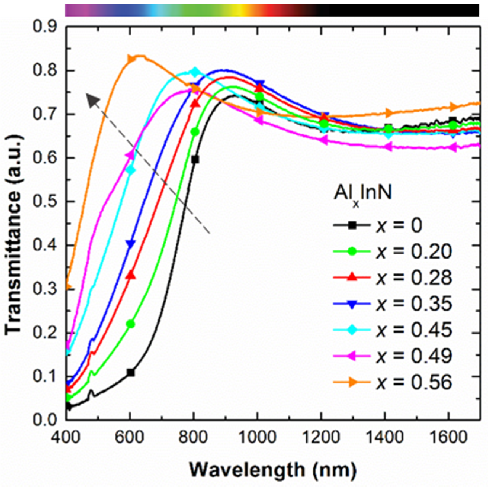
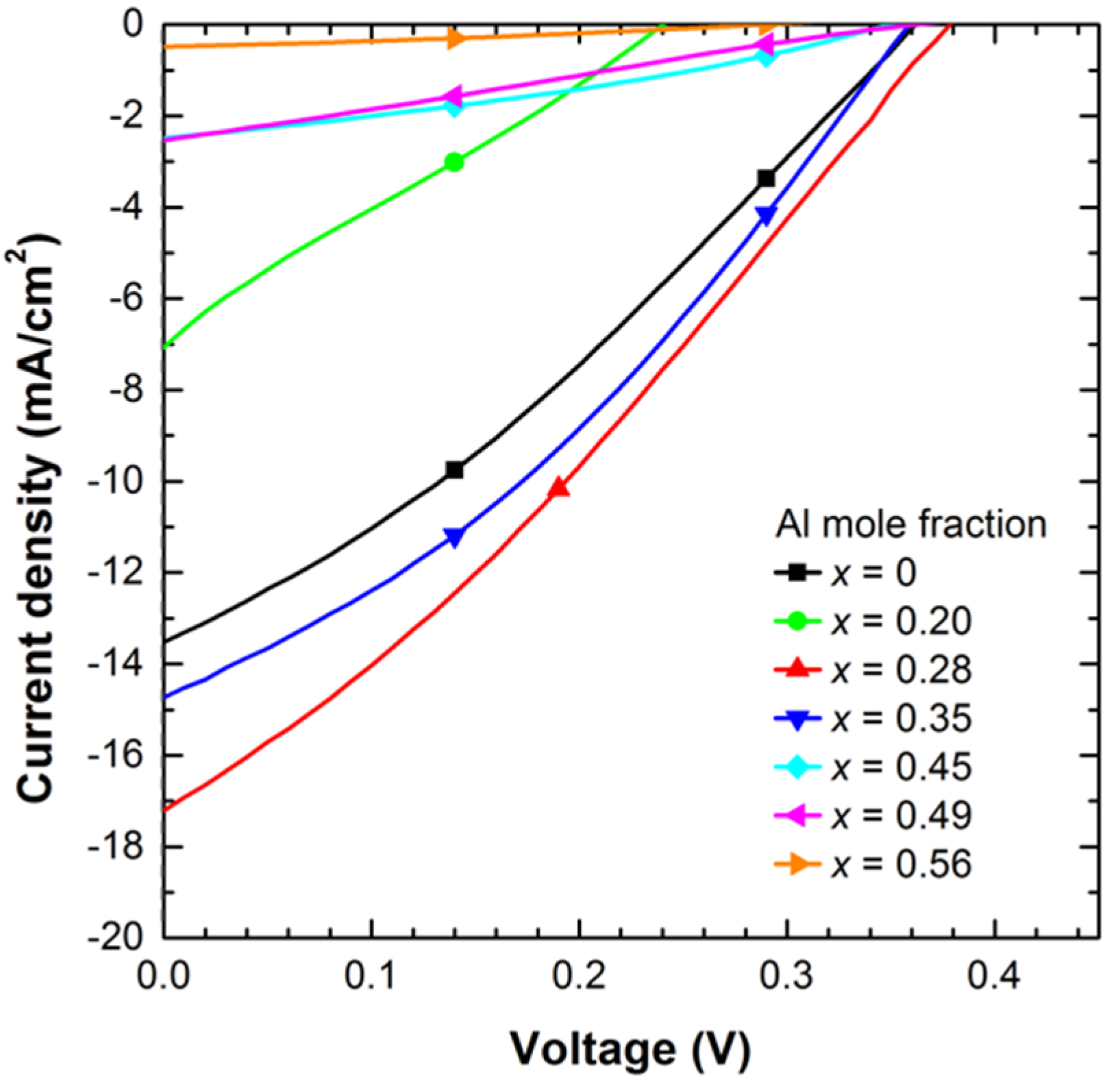
3. Results and Discussion

The structural, morphological and optical quality and properties of the AlxIn1−xN on Si (100) layers understudy was deeply analysed in reference [28]. In this report, our group demonstrated the successful deposition of high-quality and wurtzite single-phase n-type AlxIn1−xN layers with an Al mole fraction over the range of x = 0 to x = 0.56 on p-Si (100) substrates by RF magnetron sputtering. High-resolution X-ray diffraction measurements revealed that the layers own wurtzite single-phase crystalline structure oriented along the c-axis perpendicular to the sample surface. 2θ/ω scans performed in these layers show the diffraction peaks associated to the Si (100) and the AlInN (0002) reflections revealing that there is no phase separation in the AlInN alloy along the studied range of Al power supply and that no other parasitic reflections related to other phases were detected. On the other hand, the full width at half maximum of the rocking curve around the AlxIn1−xN (0002) diffraction peak decreased from ~9° to ~3° when incorporating Al to the AlxIn1−xN alloy. The root mean square surface roughness of the samples, estimated from atomic force microscopy, evolved from 20 nm for InN to 1.5 nm for Al0.56In0.44N films. For Al mole fractions equal and below 0.35, samples showed strong low- and room-temperature photoluminescence emission, which blue-shifted from 1.59 eV for InN to 1.82 eV for Al0.35In0.65N samples at 11 K. Taking into account these results, the developed n-AlxIn1−xN/p-Si junctions presented promising material properties to explore their performance operating as solar cells.
To develop efficient devices, it is of crucial importance to proper control the n-type doping. For this aim, Hall effect measurements were carried out in AlxIn1−xN films deposited on sapphire at the same time and under the same growth conditions to explore the evolution of their electrical characteristics, such as carrier concentration, layer resistivity, and carrier mobility, depending on the alloy mole fraction. As plotted in Figure 2, the resistivity of the III-nitride layers increases four orders of magnitude from 0.2 mΩ·cm to 3.4 Ω·cm for the InN (D1) to the Al0.45In0.55N samples (D5), respectively. We would like to point out that AlN material usually owns a resistivity higher than 1014 Ω·cm [29]. In this sense, the residual n-type carrier concentration decreases by almost three orders of magnitude from 7.5 × 1021 cm−3 to 1.6 × 1019 cm−3, and the carrier mobility decreases from 4.2 cm2/V·s to 0.1 cm2/V·s within the same Al mole fraction range. The responsible for the high carrier concentration of these layers are the unintentional doping coming from hydrogen and/or oxygen impurities incorporated during the sputtering deposition, and point defects like nitrogen vacancies, as previously reported [30,31,32].
Figure 3 shows the optical transmittance spectra measured in AlxIn1−xN samples deposited simultaneously on sapphire under the same deposition conditions vs the Al mole fraction x. The optical absorption band-edge blue shifts as expected with the Al content. However, transmittance measurements of layers with thickness below 100 nm never reach zero values at short wavelengths. This effect can lead to an overestimation of the estimated bandgap energy.
To overcome this, we estimated the bandgap energy from transmittance spectra measured in thick AlxIn1−xN on sapphire samples (thicknesses above 300 nm) with an Al mole fraction similar to those of the samples of this paper grown at 300 °C by RF sputtering [25]. The method to estimate the bandgap energy from transmittance measurements is described in Ref. [25]. Table 1 shows the comparison between the optical bandgap energy estimated from both set of samples, the ones of this paper (thin ones) and the ones of Ref. [25] (thick ones). From these data, we can see how the bandgap energy Eg increases from 1.73 eV to 2.56 eV according to the rise in Al mole fraction from x = 0 to 0.56, as summarized in Table 1.
It has to be noted that the high values of Eg are related to the so-called Burstein-Moss effect, i.e., the band filling of the conduction band and the blue shift of the bandgap energy of the material due to an increase of the unintentional doping (residual carrier concentrations close to 1021 cm−3) caused by impurities like oxygen and defects like nitrogen vacancies.
Current density vs voltage (J-V) curves of the processed devices were measured in the dark to analyse the electrical behaviour of the diodes. Figure 4 illustrates the J-V curves of the fabricated n-p junctions with structures D1–D7 under dark conditions pointing to a rectifying behaviour. The reverse saturation current density (J0), series and shunt resistances (Rs, Rsh) and the diode ideality factor (η) were estimated fitting experimental data to the expression: J = J0 · [exp (Vd/(η · VT)) − 1] + Vd/Rsh, where Vd is the diode voltage (Vd = V – J · Rs), and VT is the thermal voltage given by VT = kB · T/q (26 meV at room temperature).
From the results summed up in Table 2, we deduce that Rs increases from ~4.7 Ω·cm2 for InN- until ~60.3 Ω·cm2 for AlxIn1−xN-based devices (x = 0.56), probably due to the high-top n-contact resistivity present at high Al mole fractions (see Figure 1c). The gradual increase of Rsh of more than two orders of magnitude (Rsh ~ 12–3100 kΩ·cm2) and the drop of the reverse saturation current density (J0 ~ 3.6−0.15 mA/cm2) with the Al mole fraction are assigned to the improved material quality of the AlxIn1−xN layers compared to their InN counterparts, as previously demonstrated by our group [28]. At the same time, the ideality factor η drops from ~6.0 for devices with an Al mole fraction of 0.28 to ~3.0 for higher ones.
Figure 5 presents the J-V measurements of all devices under AM1.5G illumination (1 sun) carried out to evaluate their photovoltaic performance in terms of open-circuit voltage (Voc), short-circuit current density (Jsc), fill factor (FF), and power conversion efficiency (Eff.). Jsc was calculated taking into account the net area of the devices without the shadow of the top contact fingers of ~0.13 cm2.
The analysis of the photovoltaic parameters Voc, Jsc, FF and efficiency extracted from the J-V curves of Figure 5 is summarized in Table 2 as a function of the Al mole fraction x. This analysis reveals that the open-circuit voltage, the short-circuit current density and the FF increase from 0.36 V to 0.39 V, from 13.4 mA/cm2 to 17.1 mA/cm2 and from 30.7% to 31.4% for InN and Al0.28In0.72N-based devices, respectively. This improvement leads to a maximum conversion efficiency of the AlxIn1−xN on Si devices of 2.2% with 28% of Al content.
However, the high serial resistance obtained for devices growth under an Al power supply of 100 W (D2) leads to a low open-circuit voltage and short-circuit current values. This effect may be attributed to some alloy disorder on the nitride/Si interface that can be found at low Al power supplies and degrades the electrical behaviour of the junction [33].
When increasing the Al mole fraction above 28% the Voc, Jsc, and efficiency drop down to 0.29 V, 0.5 mA/cm2, and 0.05% for the Al0.56In044N-based device, respectively. This trend is contrary as expected from theory when assuming the positive influence of increasing the Al mole fraction of the alloy, hence the bandgap energy, on the open-circuit voltage and the short-circuit current of the device, as previously reported [27]. So, the drop of the photovoltaic performance of the junction for Al contents above ~30% is attributed to the deterioration of the electrical properties of the AlxIn1−xN layer (resistivity increases and carrier concentration and mobility decrease with the Al content) that increases the serial resistance of the junction and the top contact resistance of the device.
To explore the theoretical limits of performance of these n-p junctions without the above-mentioned deterioration, we have performed simulations of the J-V curves under AM1.5G illumination (1 sun) of our devices with the PC1D program [34] following the procedure described in the paper [27]. First of all, we have simulated the InN-based device to have a starting point for the next simulations of the devices with increasingly Al mole fraction. As plotted in Figure 6, we have fitted the simulated J-V curve of the InN-based device to the experimental one, taking into account the thickness of the InN layer obtained by X-ray reflection measurements [28] and the n-type carrier concentration of the InN layer of Figure 2.
Afterwards, to study the evolution of the photovoltaic performance of the devices through their J-V curves with the Al mole fraction we have kept the thickness, doping and top and bottom contact resistances fixed to the values used for the simulation of the InN (see legend of Figure 6), while we have changed the following simulation parameters with the Al mole fraction: bandgap energy, electron affinity, refractive index, dielectric constant, intrinsic concentration, and Nc/Nv ratio. We note that the PC1D program offers the possibility to take into account the experimental absorption of the layers, so in our case, we have used the transmittance data measured in AlxIn1−xN on sapphire samples grown at 300 °C with thicknesses above 300 nm and with Al mole fraction similar to those of this study [25]. From these simulations and under these particular conditions of nitride layer thickness and n-doping concentration, we can conclude that theoretically the photovoltaic performance of the AlxIn1−xN on Si (100) devices would improve with the Al content as theoretically expected (higher Voc, Jsc and conversion efficiency), achieving a maximum of Voc = 0.58 V, Jsc = 23.9 mA/cm2 and efficiency of 4.2% for n-AlxIn1−xN on p-Si devices with 50% Al.
To investigate the influence of the impinging wavelength on the photocurrent of the devices, responsivity measurements were carried out in the 375–1100 nm wavelength range. The external quantum efficiency (EQE) stands for the fraction of collected electron-hole pairs per incident photon and was estimated from these measurements as EQE = (Jop/Pop)·(hc/qλ), where Jop is the photocurrent density, Pop the optical power density impinging the device, q the electron charge, h is Planck’s constant, c is the speed of light and λ the wavelength of the incident light. The spectral evolution of the EQE curves of the devices is displayed in Figure 7. EQE values for all AlxIn1−xN on Si devices at 860 nm are 66.7% (x = 0), are 29.9% (x = 0.20), 73.8% (x = 0.28), 58.3% (x = 0.28), 20.1% (x = 0.45), 21.4% (x = 0.49), and 1.1% (x = 0.56). The best device based on an Al0.28In0.72N on Si structure presents a maximum EQE of 80% at 750 nm.
For Al mole fractions below 0.35, the device EQE presents a broad spectral response covering the full solar spectrum from the visible to the near-infrared range with a peak in the visible above the AlxIn1−xN bandgap energy followed by a photoresponse in the near-infrared with a cut-off ~1100 nm related to the Si band edge. Moreover, the band edge at short wavelengths follows the AlxIn1−xN absorption shift with the Al mole fraction as plotted the normalized EQE in the inset of Figure 7.
However, for Al mole fractions above 0.35, the EQE drops accordingly with J-V results of Figure 7 without observing any contribution coming from the Si layer. This lessening of the photovoltaic performance of the devices is attributed to the increase of the AlxIn1−xN resistivity of three orders of magnitude that lead to deterioration of the top contact performance. These results are very promising for AlxIn1−xN on Si structures working as solar cells. Nevertheless, the degradation of the photovoltaic performance for devices with Al contents above 35% need to be overcome. For this aim, new strategies should be incorporated, such as doping the AlxIn1−xN layer with Si and/or introducing a thin highly n-doped InN layer on top of the junction to improve the contact resistance.

4. Conclusions

Photovoltaic devices based on n-AlxIn1−xN on p-Si (100) hetero-junction solar cells with Al content ranging from 0% to 56% were fabricated by RF sputtering. The variation on the Al content leads to an evolution of the optical bandgap edge from 1.73 to 2.56 eV. Increasing the Al leads also to a 7-fold increase of the top n-contact resistance due to the higher AlxIn1-xN resistivity and the drop of the n-type carrier concentration. Best results achieved for solar cells with x = 0.28 are Voc = 0.39 V, Jsc = 17.1 mA/cm2, and FF = 31.4% under AM1.5G equivalent illumination (1 sun), pointing to a conversion efficiency of 2.12% without any top/back coating or surface treatment. For Al contents above 28 %, the photovoltaic performance is gradually reduced due to the strong top contact resistance, agreeing with the EQE of the devices, which drastically drops. Theoretical simulations of these structures point to a maximum of Voc = 0.58 V, Jsc = 23.9 mA/cm2, and efficiency of 4.2% for n-AlxIn1−xN on p-Si devices with 50% Al and a III-nitride resistivity in the ≈10−4 Ω·cm range.

Author Contributions

Conceptualization, S.V.-F. and F.B.N.; methodology, S.V.-F. and F.B.N.; software, R.B. and S.V.-F.; validation, J.O., A.F.B. and F.B.N.; formal analysis, R.B., J.O. and A.D.-L.; investigation, R.B., S.V.-F., J.O., A.D.-L., A.F.B. and F.B.N.; resources, R.B.; writing—original draft preparation, S.V.-F. and R.B.; writing—review and editing, J.O., A.D.-L., A.F.B. and F.B.N.; visualization, S.V.-F. and R.B.; supervision, S.V.-F. and F.B.N.; project administration, S.V.-F. and F.B.N.; funding acquisition, S.V.-F. and F.B.N. All authors have read and agreed to the published version of the manuscript.

Funding

This research was funded by the national projects from the Ministry of Research and Innovation TEC2017-84378-R and NERA (RTI2018-101037-B-I00); the projects from the Comunidad de Madrid SINFOTON2-CM (P2018/NMT-4326), MADRID-PV2 (P-2018/EMT-4308) and SOLA (CM/JIN/2019-013); the projects from the University of Alcalá ANIS (CCG2018/EXP-042) and PISA (CCG19/IA-005); and by the FEDER program. R. Blasco acknowledges the financial support of his contract associated with the Ramon y Cajal Fellowship RYC-2013-14084.

Conflicts of Interest

The authors declare no conflict of interest. The funders had no role in the design of the study; in the collection, analyses, or interpretation of data; in the writing of the manuscript, or in the decision to publish the results.

References

  1. Palmstrom, A.F.; Eperon, G.E.; Leijtens, T.; Prasanna, R.; Habisreutinger, S.N.; Nemeth, W.; Gaulding, E.A.; Dunfield, S.P.; Reese, M.; Nanayakkara, S.; et al. Enabling flexible all-perovskite tandem solar cells. Joule 2019, 3, 2193. [Google Scholar] [CrossRef]
  2. Veinberg-Vidal, E.; Vauche, L.; Medjoubi, K.; Weick, C.; Besançon, C.; Garcia-Linares, P.; Datas, A.; Kaminski-Cachopo, A.; Voarino, P.; Mur, P.; et al. Characterization of dual-junction III-V on Si tandem solar cells with 23.7% efficiency under low concentration. Prog. Photovolt. Res. Appl. 2019, 27, 652. [Google Scholar] [CrossRef]
  3. Bhuiyan, A.G.; Sugita, K.; Hashimoto, A.; Yamamoto, A. InGaN solar cells: Present state of the art and important challenges. IEEE J. Photovolt. 2012, 2, 3. [Google Scholar] [CrossRef]
  4. Irvine, S.; Capper, P. Metalorganic Vapor Phase Epitaxy (MOVPE): Growth, Materials Properties and Applications; John Wiley & Sons: Hoboken, NJ, USA, 2019. [Google Scholar]
  5. Dinh, D.V.; Hu, N.; Honda, Y.; Amano, H.; Pristovsek, M. Indium incorporation and optical properties of polar, semipolar and nonpolar InAlN. Semicond. Sci. Technol. 2020, 35, 035004. [Google Scholar] [CrossRef]
  6. Borovac, D.; Sun, W.; Song, R.; Wierer, J.J., Jr.; Tansu, N. On the thermal stability of nearly lattice-matched AlInN films grown on GaN via MOVPE. J. Cryst. Growth 2020, 533, 125469. [Google Scholar] [CrossRef]
  7. Miyoshi, M.; Yamanaka, M.; Egawa, T.; Takeuchi, T. Epitaxial growth and characterization of approximately 300-nm-thick AlInN films nearly lattice-matched to c-plane GaN grown on sapphire. Appl. Phys. Express 2018, 11, 051001. [Google Scholar] [CrossRef]
  8. Engel, Z.; Clinton, E.A.; Matthews, C.M.; Doolittle, W.A. Controlling surface adatom kinetics for improved structural and optical properties of high indium content aluminum indium nitride. J. Appl. Phys. 2020, 127, 125301. [Google Scholar] [CrossRef]
  9. Gacevic, Z.; Fernández-Garrido, S.; Rebled, J.M.; Estrade, S.; Peiro, F.; Calleja, E. High quality InAlN single layers lattice-matched to GaN grown by molecular beam epitaxy. Appl. Phys. Lett. 2011, 99, 031103. [Google Scholar] [CrossRef] [Green Version]
  10. Terashima, W.; Che, S.-B.; Ishitani, Y.; Yoshikawa, A. Growth and characterization of AlInN ternary alloys in whole composition range and fabrication of InN/AlInN multiple quantum wells by RF molecular beam epitaxy. Jpn. J. Appl. Phys. 2006, 45, L539. [Google Scholar] [CrossRef]
  11. Izyumskaya, N.; Avrutin, V.; Ding, K.; Özgür, Ü.; Morkoç, H.; Fujioka, H. Emergence of high quality sputtered III-nitride semiconductors and devices. Semicond. Sci. Technol. 2019, 34, 093003. [Google Scholar] [CrossRef]
  12. Lv, W.; Shen, L.; Liu, J.; Chen, J.; Wu, L.; Qi, D.; Zhang, G.; Li, X. Mechanical properties of single-phase Al1-xInxN films across the compositional range (0 ≤ x ≤ 0.7) grown by radio-frequency magnetron sputtering. Appl. Surf. Sci. 2020, 504, 144335. [Google Scholar] [CrossRef]
  13. Han, Q.; Duan, C.; Du, G.; Shi, W.; Ji, L. Magnetron sputter epitaxy and characterization of wurtzite AlInN on Si (111) substrates. J. Electron. Mater. 2010, 39, 489. [Google Scholar] [CrossRef]
  14. Núñez-Cascajero, A.; Blasco, R.; Valdueza-Felip, S.; Montero, D.; Olea, J.; Naranjo, F.B. High quality Al0.37In0.63N layers grown at low temperature (<300 °C) by radio-frequency sputtering. Mater. Sci. Semicond. Process 2019, 100, 8. [Google Scholar]
  15. Núñez-Cascajero, A.; Monteaguso-Lerma, L.; Valdueza-Felip, S.; Navío, C.; Monroy, E.; Gonzalez-Herráez, M.; Naranjo, F.B. In-rich AlxIn1−xN grown by RF-sputtering on sapphire: From closely-packed columnar to high-surface quality compact layers. J. Phys. D Appl. Phys. 2017, 50, 65101. [Google Scholar] [CrossRef]
  16. Núñez-Cascajero, A.; Valdueza-Felip, S.; Blasco, R.; Mata, M.; Molina, S.I.; González-Herráez, M.; Monroy, E.; Naranjo, F.B. Quality improvement of AlInN/p-Si heterojunctions with AlN buffer layer deposited by RF-sputtering. J. Alloys Compd. 2018, 769, 824. [Google Scholar] [CrossRef]
  17. Núñez-Cascajero, A.; Monteagudo-Lerma, L.; Valdueza-Felip, S.; Navío, C.; Monroy, E.; Gonzalez-Herráez, M.; Naranjo, F.B. Study of high In-content AlInN deposition on p-Si(111) by RF-sputtering. Jpn. J. Appl. Phys. 2016, 55, 05FB07. [Google Scholar] [CrossRef]
  18. Lannoo, M. The role of dangling bonds in the properties of surfaces and interfaces of semiconductors. Rev. Phys. Appl. 1990, 25, 887. [Google Scholar] [CrossRef]
  19. Yodo, T.; Ando, H.; Nosei, D.; Harada, Y. Growth and characterization of InN heteroepitaxial layers grown on Si substrates by ECR-Assisted MBE. Phys. Status Solidi B 2001, 228, 21. [Google Scholar] [CrossRef]
  20. Chen, W.C.; Wu, Y.H.; Peng, C.Y.; Hsiao, C.N.; Chang, L. Effect of In/Al ratios on structural and optical properties of InAlN films grown on Si (100) by RF-MOMBE. Nanoscale Res. Lett. 2014, 9, 204. [Google Scholar] [CrossRef] [Green Version]
  21. He, H.; Yongge, C.; Renli, F.; Hai, W.; Jiquan, H.; Changgang, H.; Wang, M.; Zhonghua, D. Structure and optical properties of InN and InAlN films grown by rf magnetron sputtering. J. Mater. Sci. Mater. 2010, 21, 676. [Google Scholar] [CrossRef]
  22. Afzal, N.; Devarajan, M.; Subramani, S.; Ibrahim, K. Structural and surface analysis of AlInN thin films synthesized by elemental stacks annealing. Mater. Res. Express 2014, 1, 026403. [Google Scholar] [CrossRef]
  23. Liu, H.F.; Tan, C.C.; Dalapati, G.K.; Chi, D.Z. Magnetron-sputter deposition of high-indium-content n-AlInN thin film on p-Si (001) substrate for photovoltaic applications. J. Appl. Phys. 2012, 112, 063114. [Google Scholar] [CrossRef]
  24. Valdueza-Felip, S.; Núñez-Cascajero, A.; Blasco, R.; Montero, D.; Grenet, L.; Mata, M.; Fernández, S.; Marcos, L.R.; Molina, S.I.; Olea, J.; et al. Influence of the AlN interlayer thickness on the photovoltaic properties of in-rich AlInN on Si heterojunctions deposited by RF sputtering. Aip Adv. 2018, 8, 115315. [Google Scholar] [CrossRef] [Green Version]
  25. Blasco, R. Development of solar cells based on AlInN on Si heterojunctions grown by RF-sputtering. Ph.D. Thesis, University of Alcalá, Alcalá de Henares, Spain, March 2020. [Google Scholar]
  26. Blasco, R.; Núñez-Cascajero, A.; Jiménez-Rodríguez, M.; Montero, D.; Grenet, L.; Olea, J.; Naranjo, F.B.; Valdueza-Felip, S. Influence of the AlInN thickness on the photovoltaic characteristics of AlInN on Si solar cells deposited by RF sputtering. Phys. Status Solidi A 2018, 216, 1800494. [Google Scholar] [CrossRef]
  27. Blasco, R.; Naranjo, F.B.; Valdueza-Felip, S. Design of AlInN on silicon heterojunctions grown by sputtering for solar devices. Curr. Appl. Phys. under review.
  28. Blasco, R.; Valdueza-Felip, S.; Montero, D.; Olea, J.; Naranjo, F.B. Low-to-mid Al content (x~0-0.56) AlxIn1-xN layers deposited on Si (100) by RF sputtering. Phys. Status Solidi B 2020, 257, 1900575. [Google Scholar] [CrossRef]
  29. Final Advanced Materials. Aluminium Nitride Substrate. Available online: www.final-materials.com/gb/383-aluminium-nitride-substrate (accessed on 2 May 2020).
  30. Darakchieva, V.; Barradas, N.P.; Xie, M.Y.; Lorenz, K.; Alves, E.; Schubert, M.; Persson, P.O.; Giuliani, F.; Munnik, F.; Hsiao, C.L.; et al. Role of impurities and dislocations for the unintentional n-type conductivity in InN. Physica B 2009, 404, 4476. [Google Scholar] [CrossRef]
  31. Darakchieva, V.; Lorenz, K.; Barradas, N.P.; Alves, E.; Monemar, B.; Schubert, M.; Franco, N.; Hsiao, C.L.; Chen, L.C.; Schaff, W.J.; et al. Hydrogen in InN: A ubiquitous phenomenon in molecular beam epitaxy grown material. Appl. Phys. Lett. 2010, 96, 081907. [Google Scholar] [CrossRef] [Green Version]
  32. Wu, J. When group-III nitrides go infrared: New properties and perspectives. J. Appl. Phys. 2009, 106, 11101. [Google Scholar] [CrossRef]
  33. Núñez-Cascajero, A. Development of Nitrides Based on InN for Sensor Applications. Ph.D. Thesis, University of Alcalá, Alcalá de Henares, Spain, June 2017. [Google Scholar]
  34. PC1D—Software for modelling a solar cell. Available online: www.engineering.unsw.edu.au/energy-engineering/research/software-data-links/pc1d-software-for-modelling-a-solar-cell (accessed on 2 May 2020).
Figure 1. (a) Schematic description of an AlxIn1−xN on Si hetero-junction solar cell. (b) Top-view image of a representative device with ~0.7 cm2 area. (c) Variation of the top n-contact resistance deposited on the AlxIn1−xN layer vs the power applied to the Al target (PAl) used for the AlxIn1−xN growth.
Materials 13 02336 g001
Figure 2. Dependence of the room temperature carrier concentration and resistivity of the AlxIn1−xN on sapphire films vs the Al mole fraction x. For x > 0.45 electrical measurements were not reliable due to the high resistivity of the layers, being above the resolution of the Hall effect setup.
Materials 13 02336 g002
Figure 3. Optical transmission spectra of the AlxIn1−xN on sapphire samples vs the Al mole fraction.
Materials 13 02336 g003
Figure 4. Current density vs voltage curves in the dark of the AlxIn1−xN on Si (100) devices vs the Al mole fraction x.
Materials 13 02336 g004
Figure 5. Current density vs voltage curves of the AlxIn1−xN on Si (100) devices under AM1.5G illumination (1 sun) vs the Al mole fraction x.
Materials 13 02336 g005
Figure 6. Comparison of the experimental J-V curve of the InN on Si device with the simulated one with PC1D program taking into account the simulation parameters from the inset.
Materials 13 02336 g006
Figure 7. Influence of the Al mole fraction x on the EQE of the AlxIn1−xN on Si (100) devices as a function of the wavelength. Inset: detail of the normalized EQE of devices with x ≤ 0.35.
Materials 13 02336 g007
Table 1. Summary of the optical bandgap energy (Eg) of the AlxIn1−xN on Si devices.
SamplePAl (W)xEg of Thin Samples (eV)Eg of Thick Samples (eV)
D1001.741.73
D21000.201.87-
D31250.282.031.79
D41500.352.082.13
D51750.452.24-
D62000.492.382.27
D72250.562.572.56
Table 2. Summary of the electrical performance of the AlxIn1−xN on Si (100) devices. The area of the devices was estimated taking into account the area of the top n-contact of ~0.13 cm2.
SamplexArea (cm2)Rs
(Ω·cm2)
Rsh
(kΩ·cm2)
J0 @-1V
(µA/cm2)
ηVOC
(V)
JSC
(mA/ cm2)
FF (%)Eff. (%)EQE at 860 nm (%)
D100.674.7123.602.80.3613.430.71.4966.7
D20.200.6058.99800.043.80.257.321.60.4029.9
D30.280.622.11800.416.00.3917.131.42.1273.8
D40.350.7012.3214.404.70.3614.633.81.7758.3
D50.450.6014.11800.314.20.352.532.80.2820.1
D60.490.4818.03200.233.40.362.525.20.2321.4
D70.560.6560.331000.153.00.290.4731.00.051.1

