Texture and Microstructural Features at Different Length Scales in Inconel 718 Produced by Selective Laser Melting


 , , ,
, , , 
Abstract
1. Introduction
2. Materials and Methods
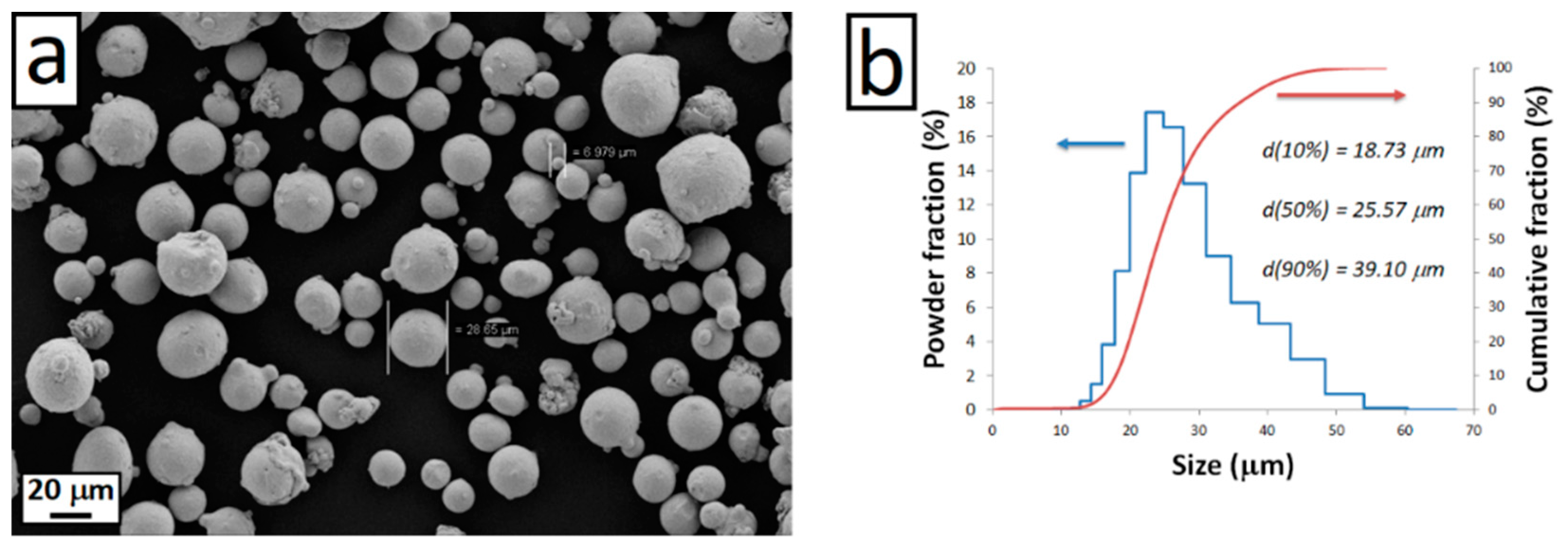
2.1. Manufacturing Procedure
2.2. Processing Parameters Optimization Procedure
2.3. Microstructural Characterization of the As-Built State
2.4. Microstructural Evolution Investigation during Aging
3. Results
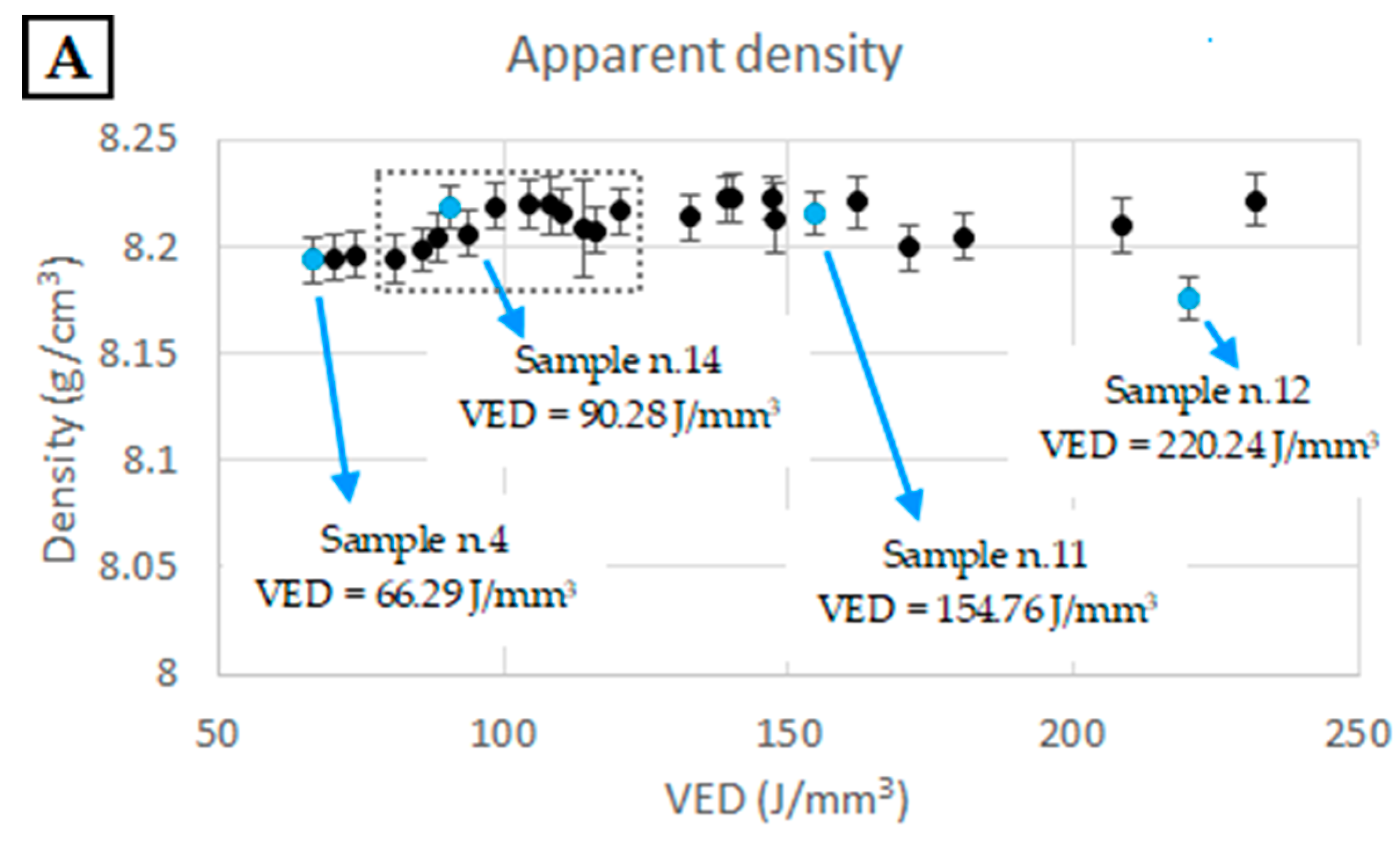
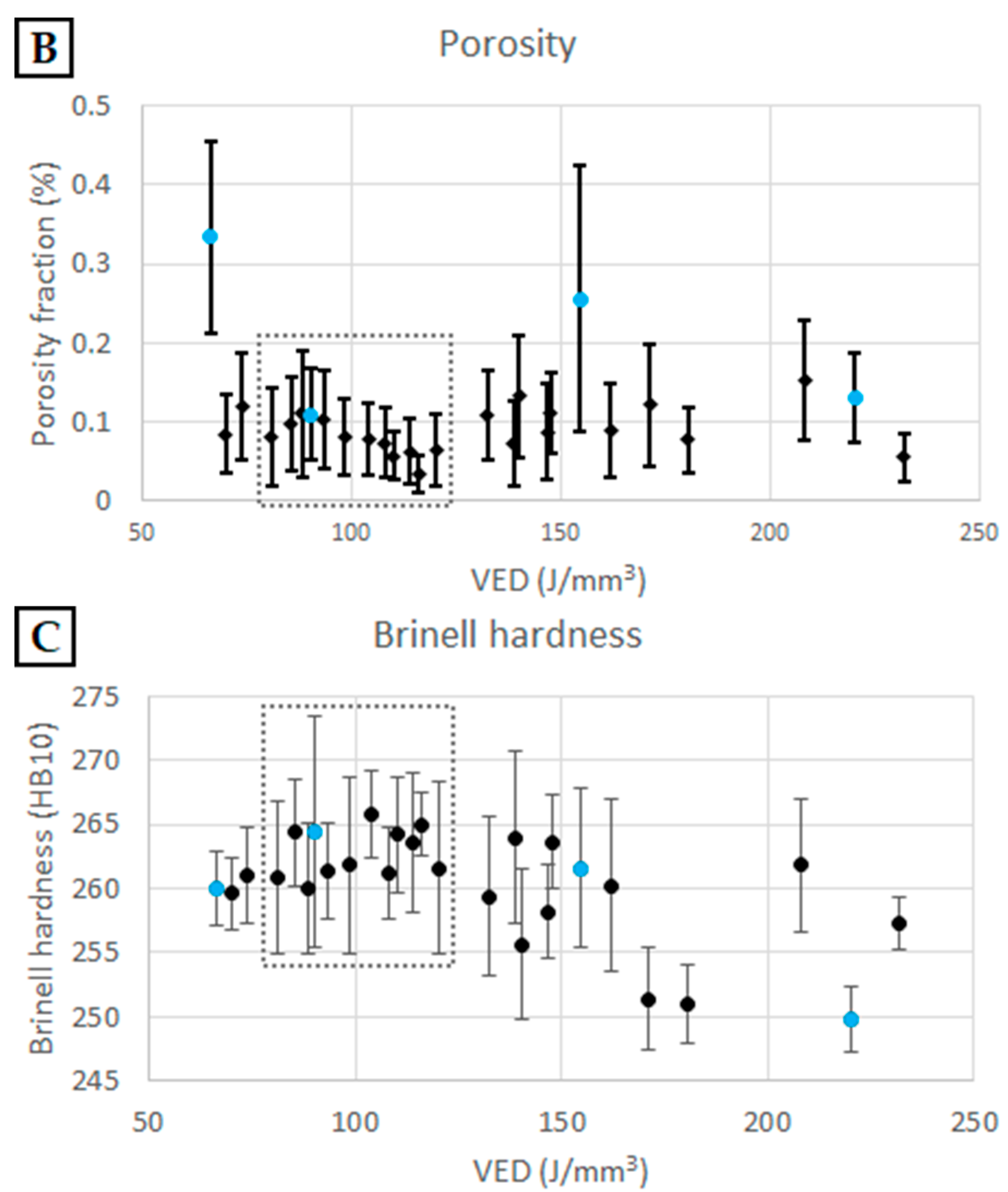
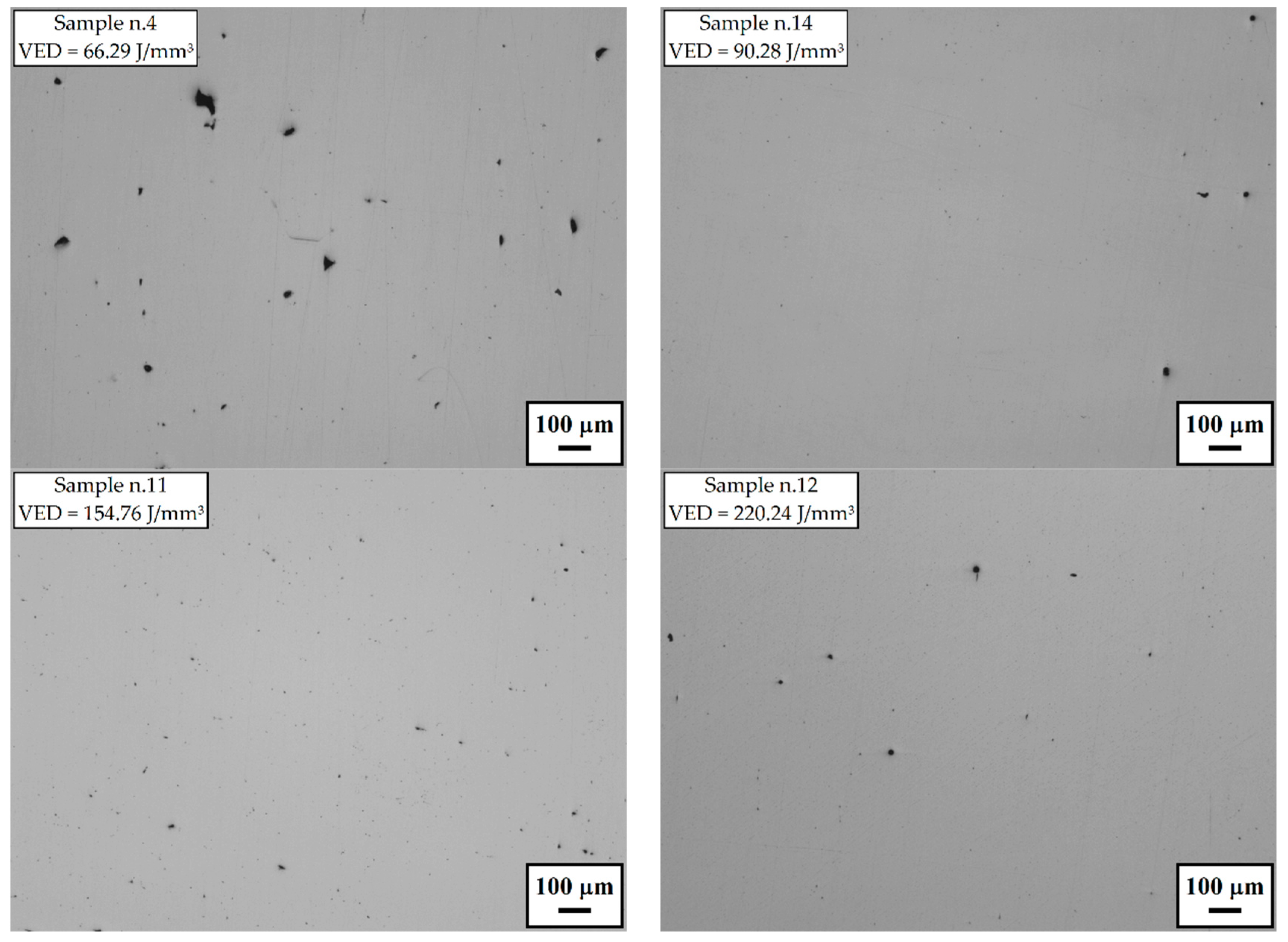
3.1. Optimization of the Process Parameters
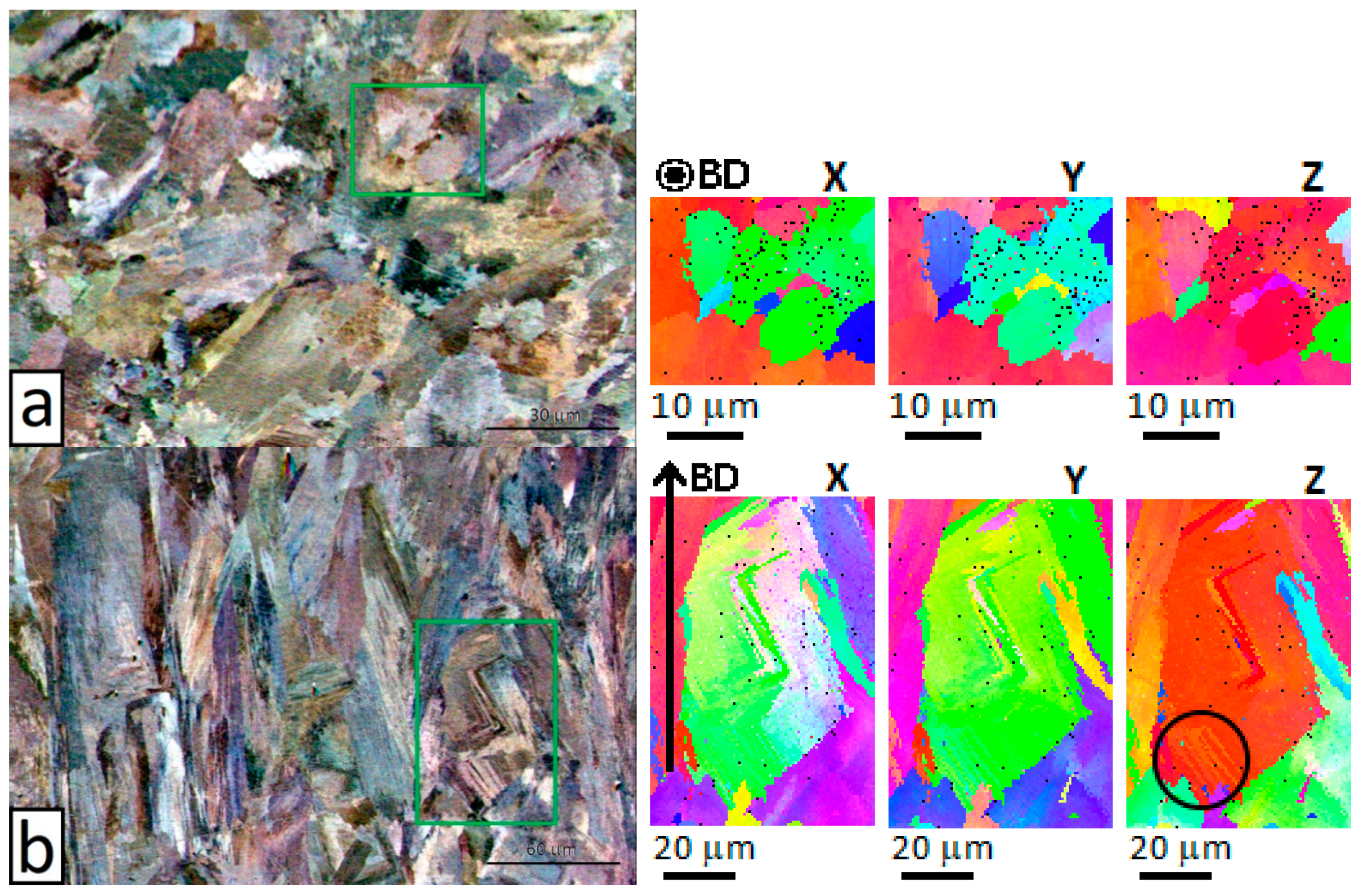
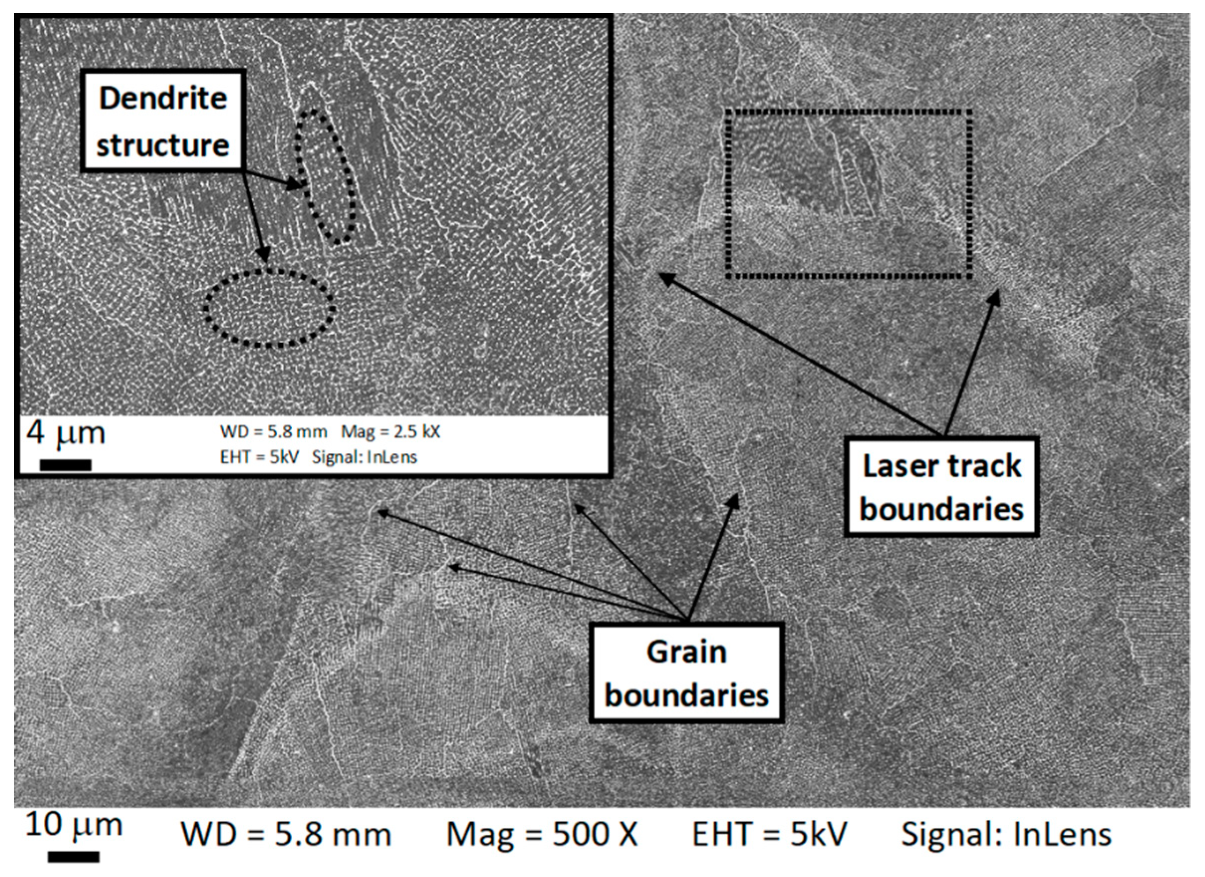
3.2. Grains and Laser-Related Microstructure (10−3–10−4 m)
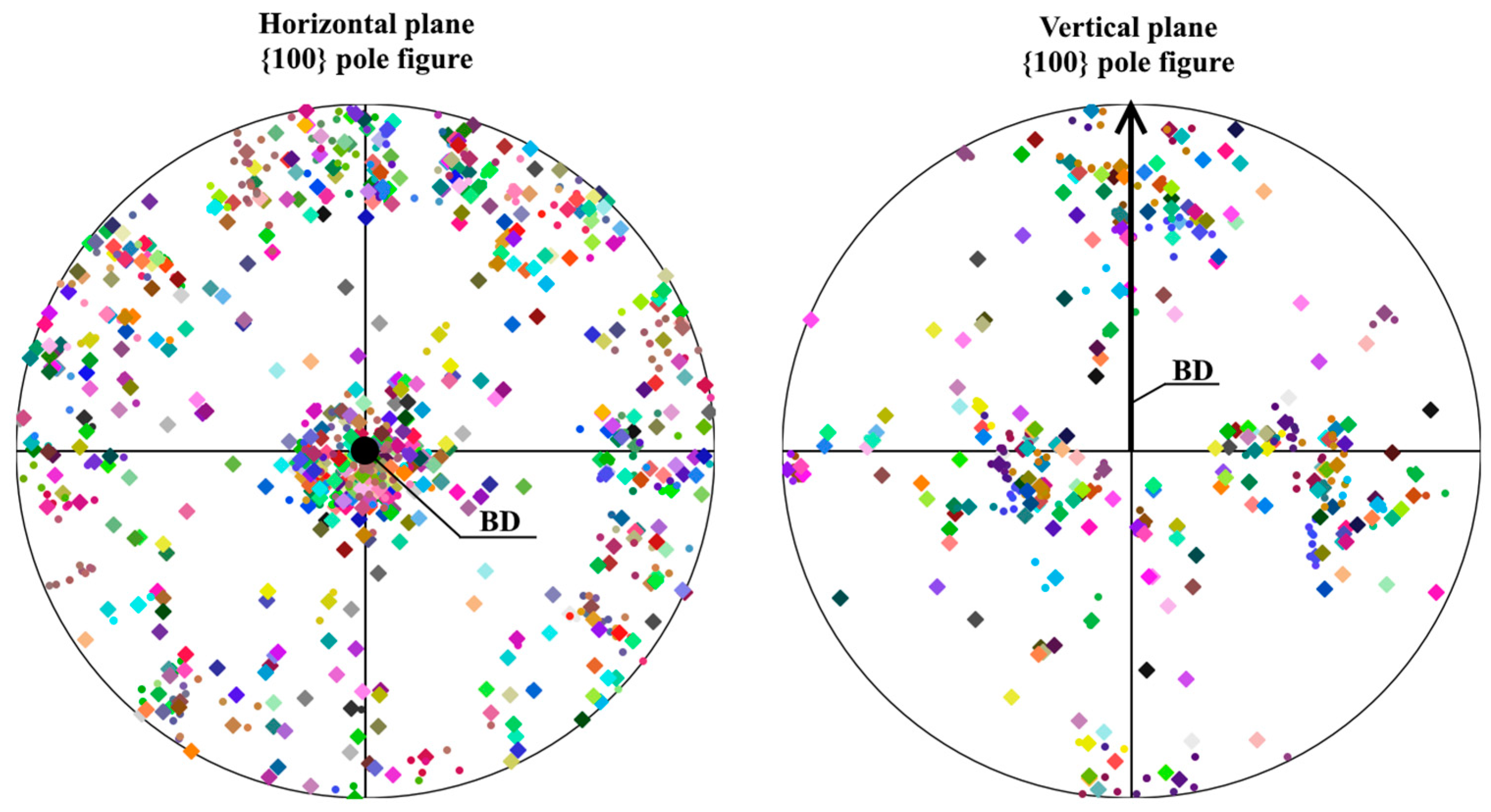
3.3. Crystallographic Texture (10−4–10−5 m)
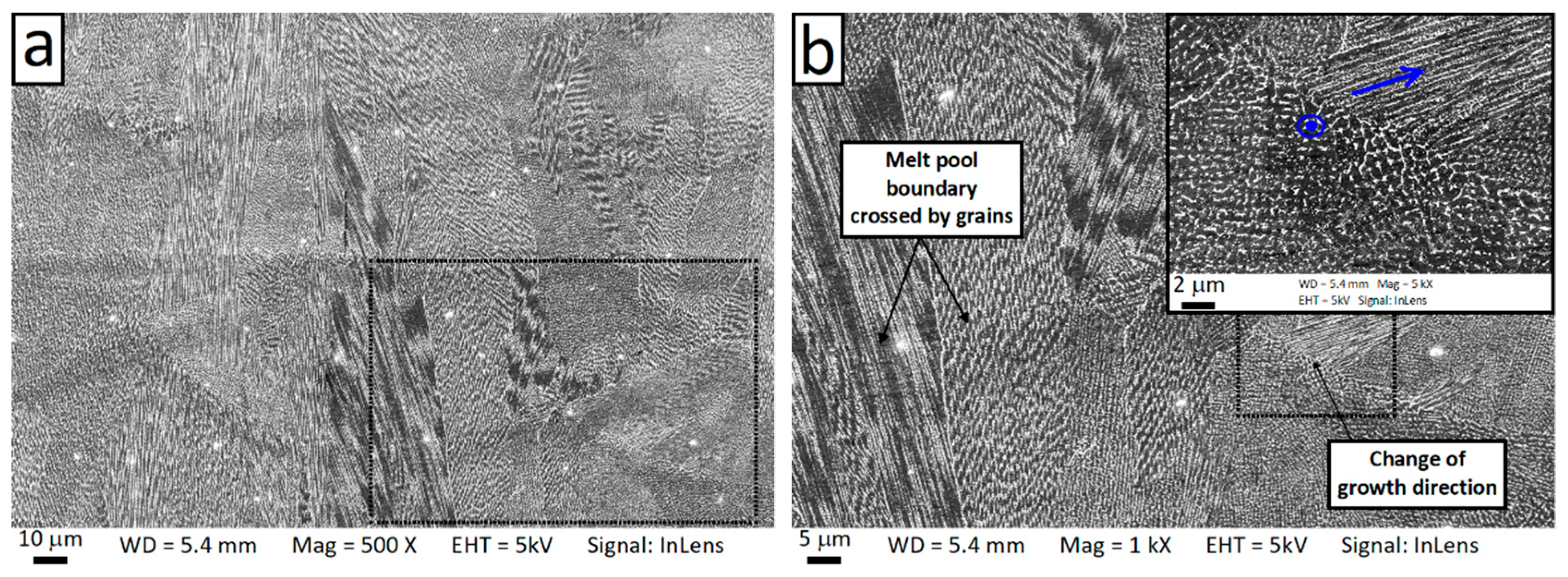
3.4. Intragranular Dendrites (10−5–10−6 m)
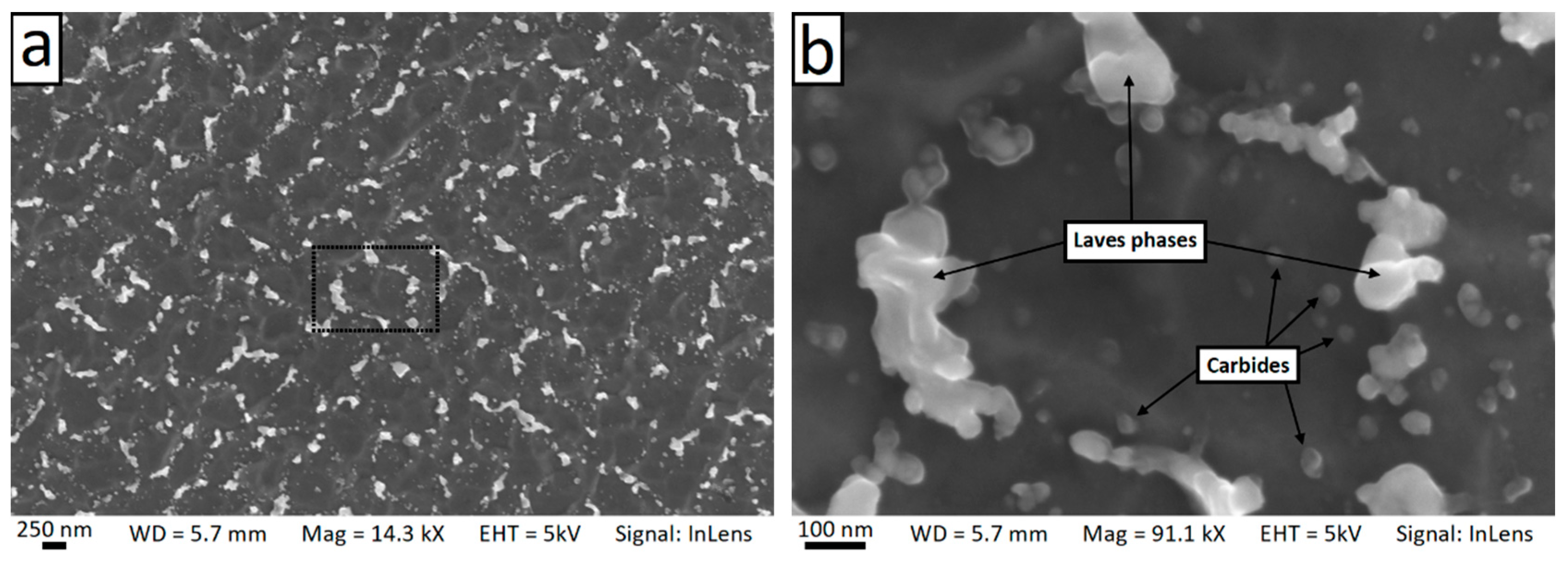
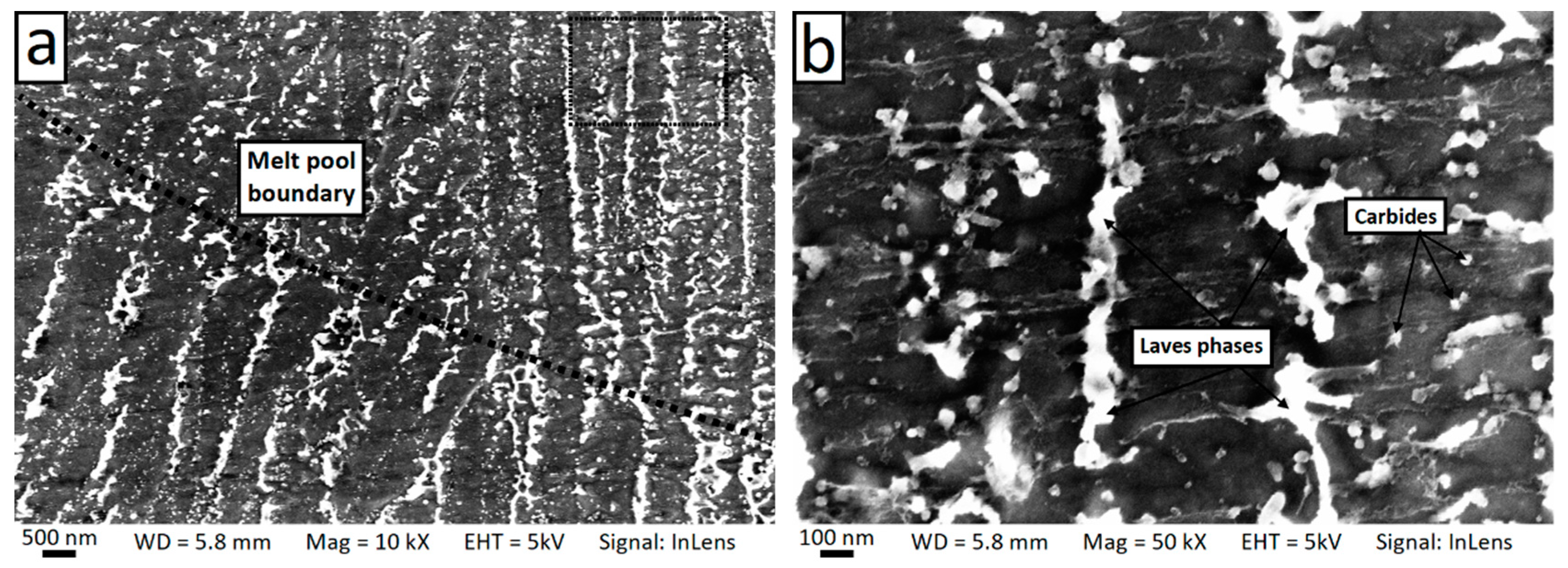
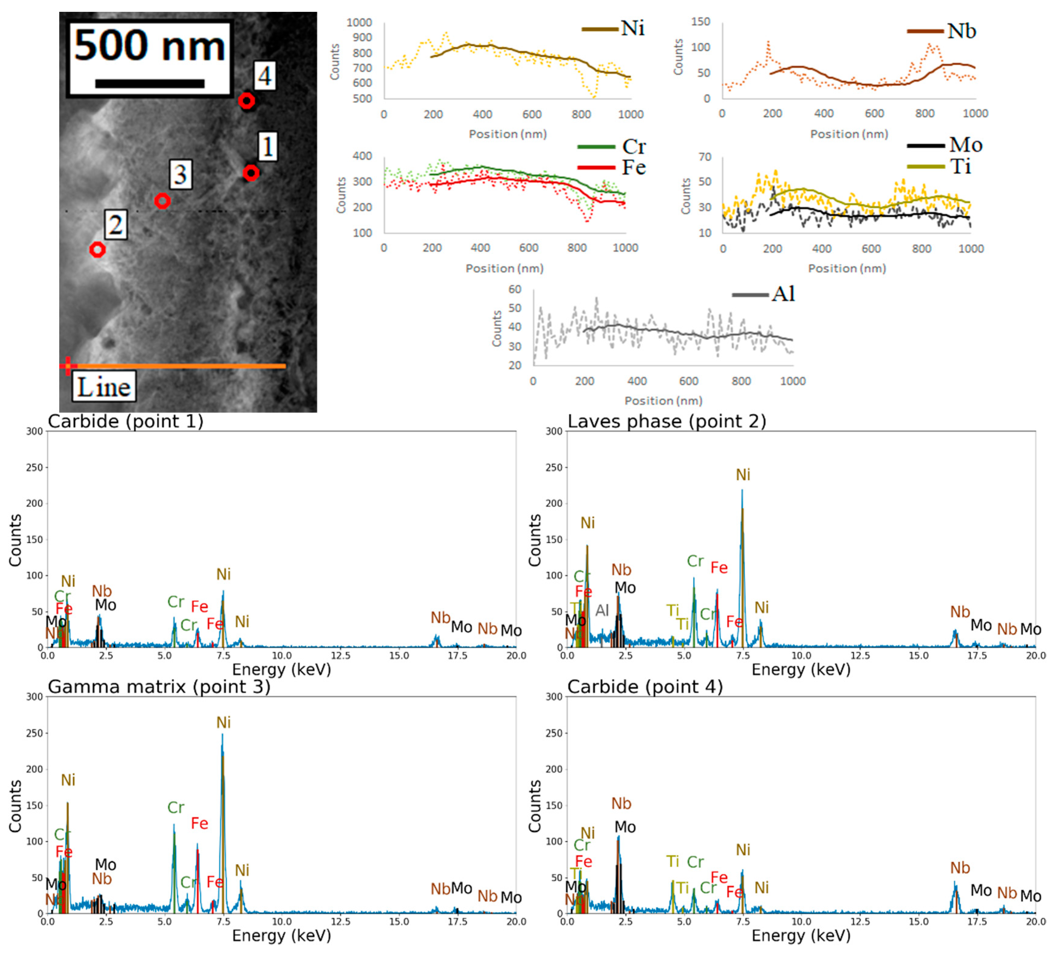
3.5. Microsegregation, Interdendrite, and Intradendrite Phases (10−6–10−8 m)
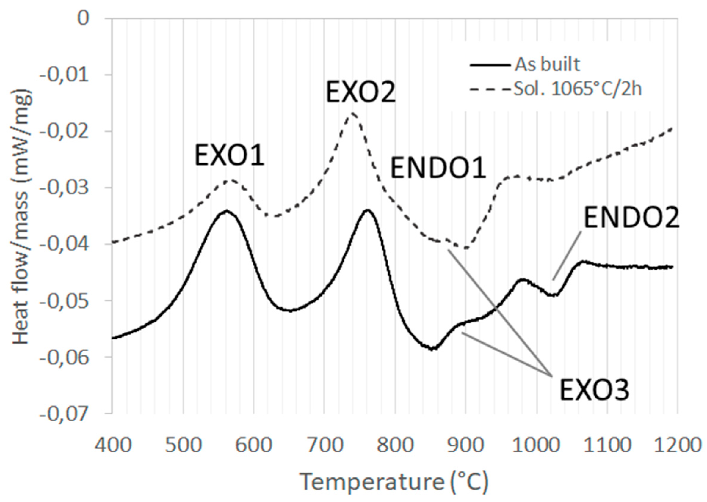
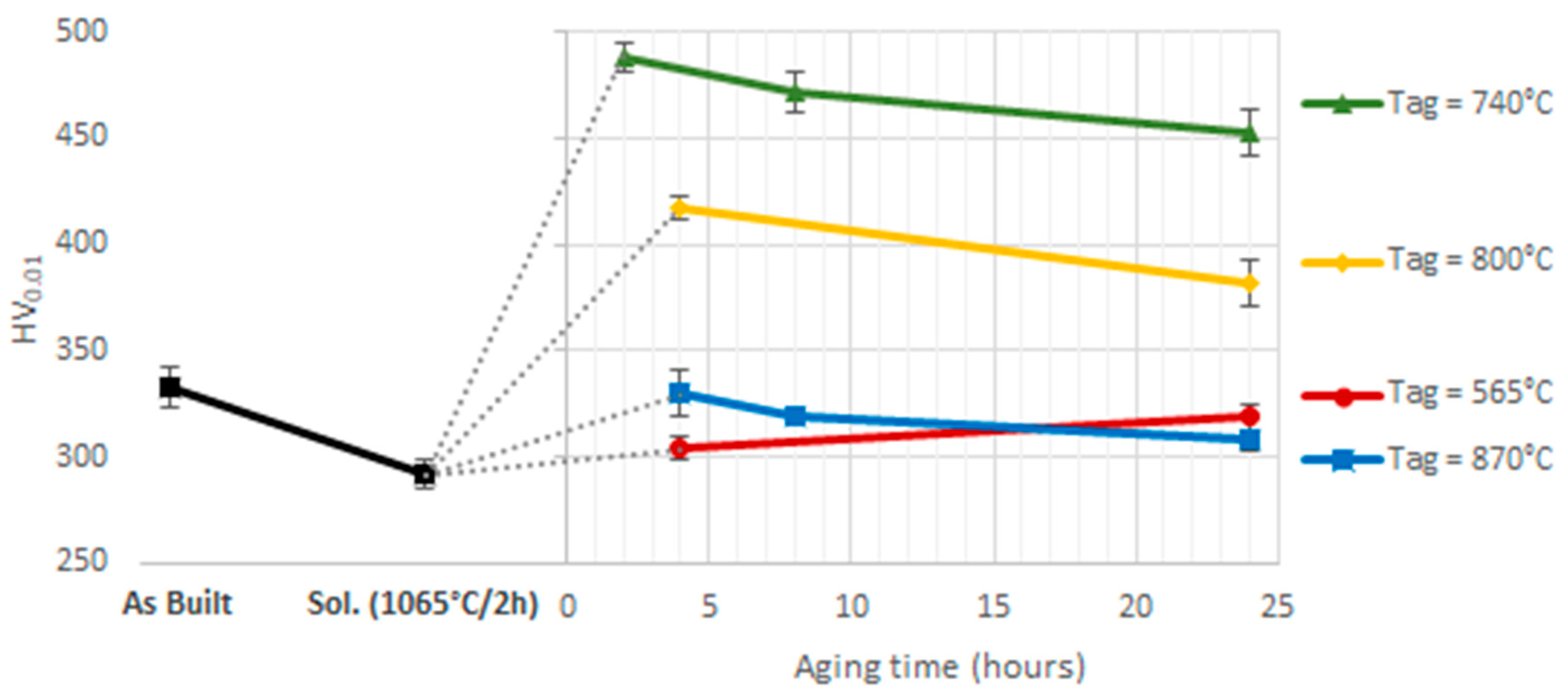
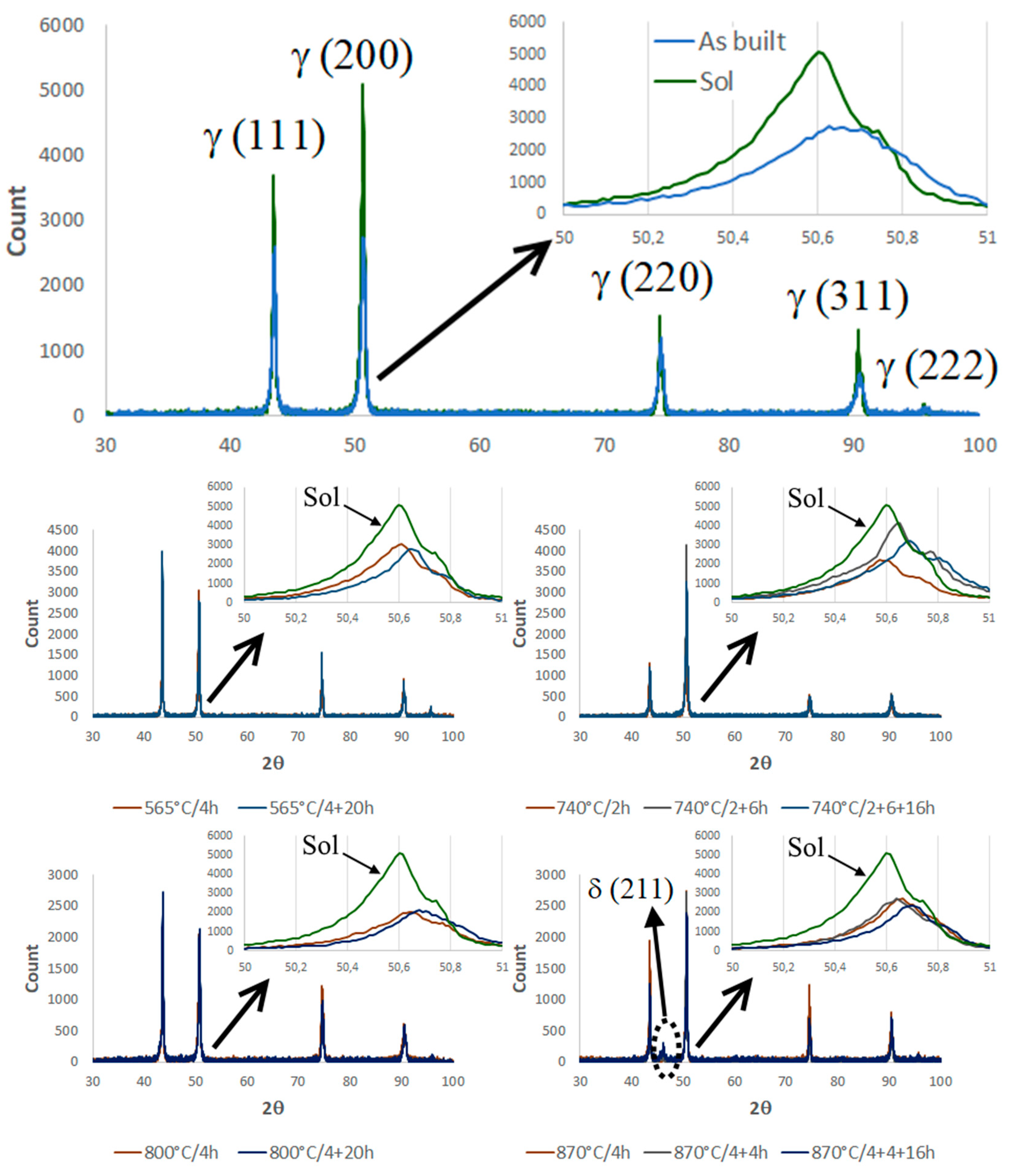
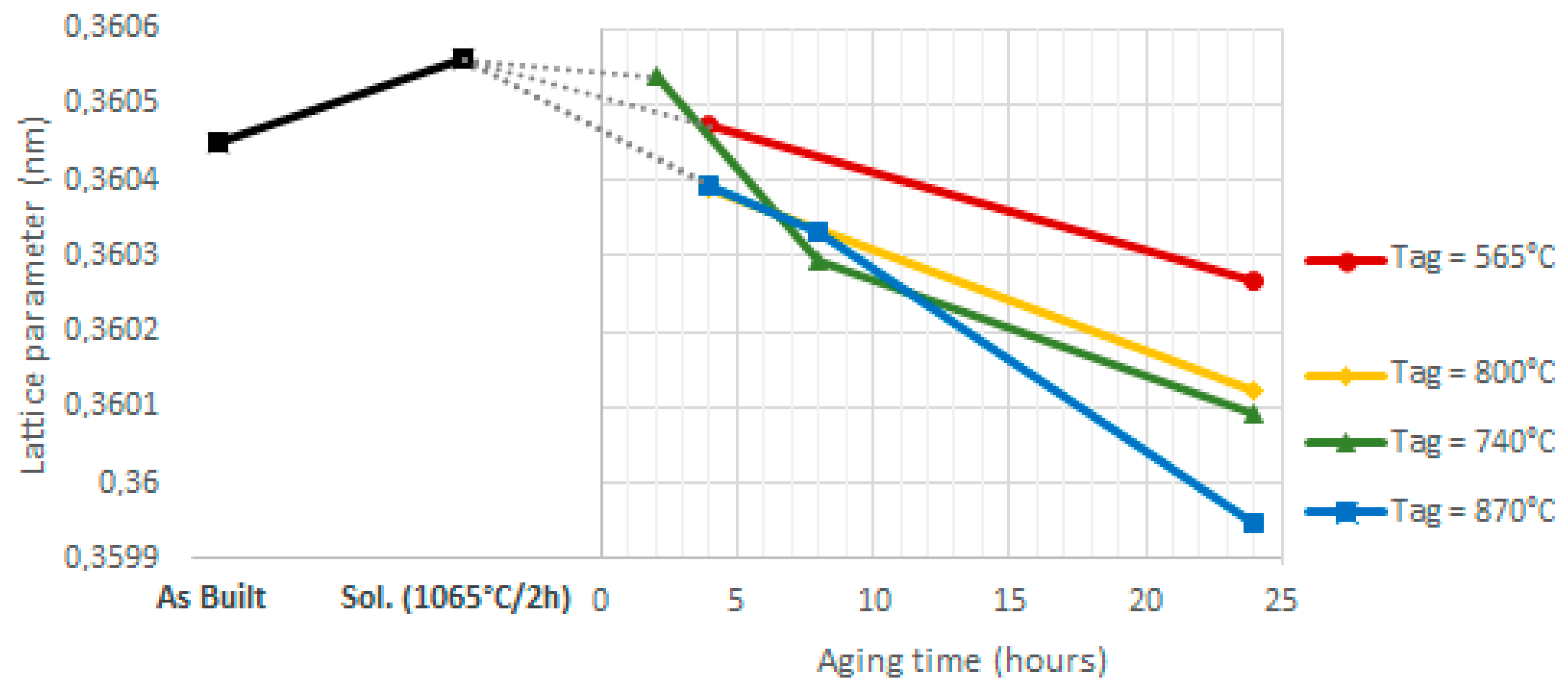
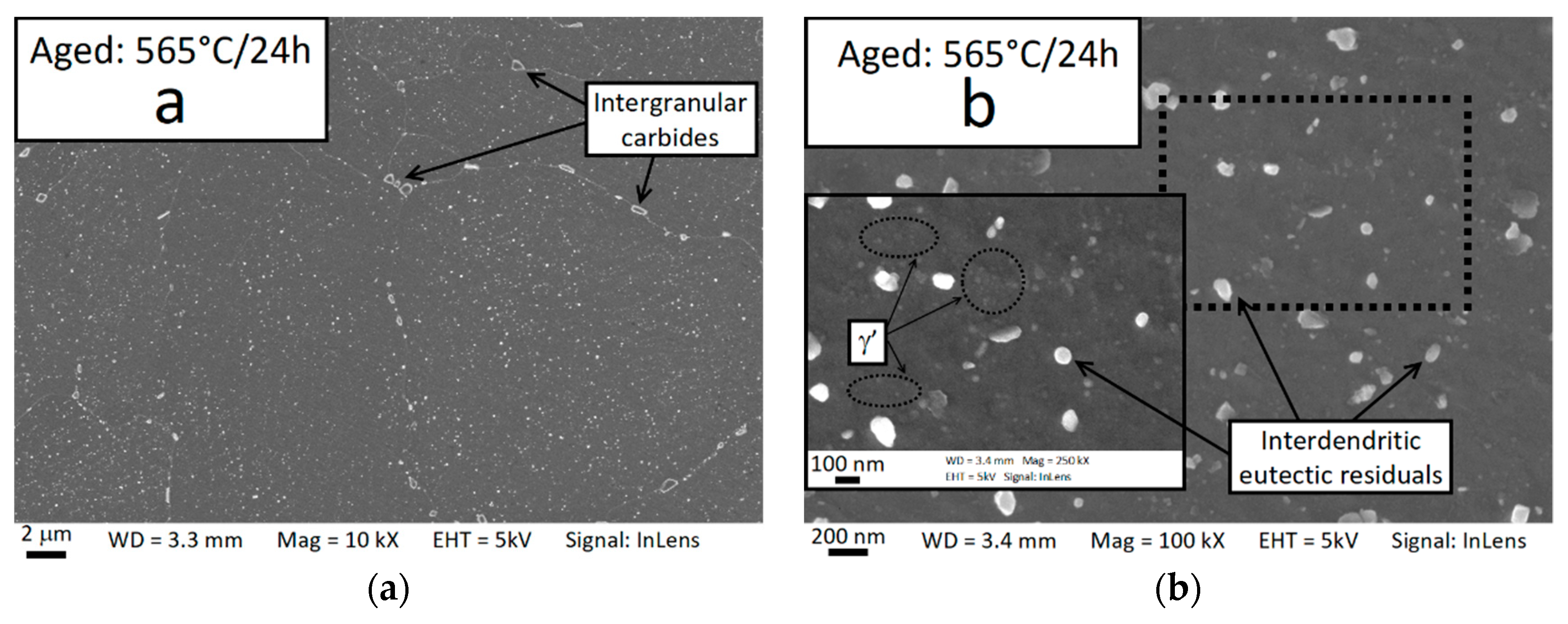
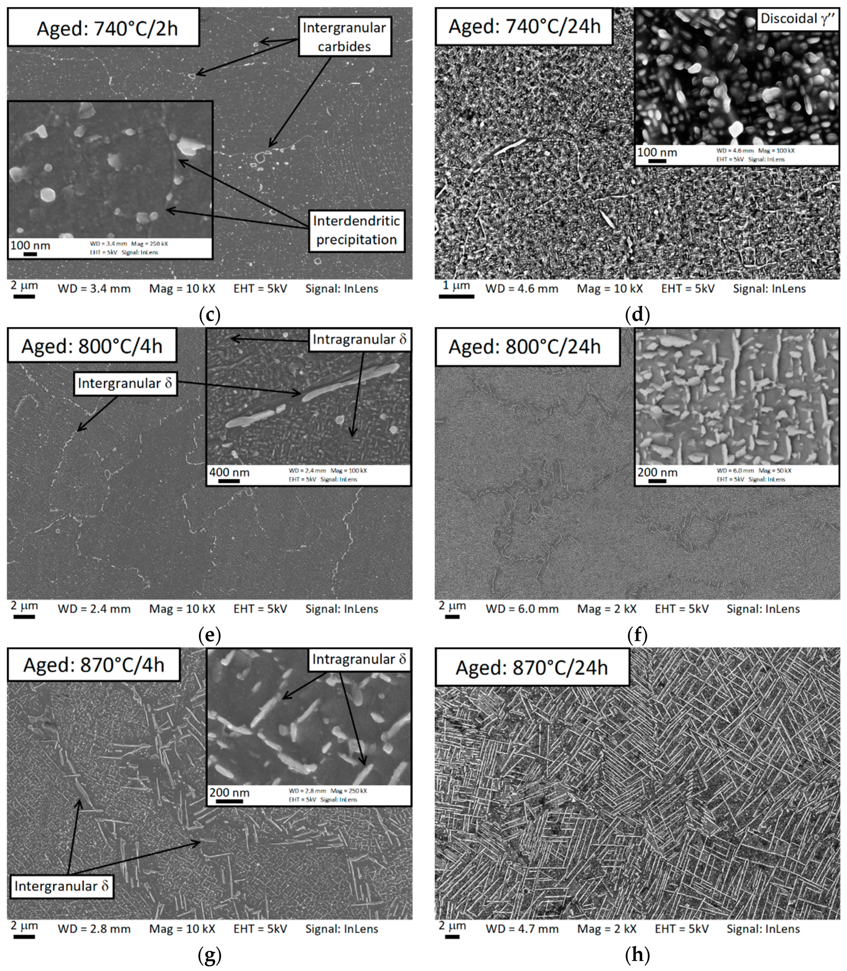
3.6. Aged State Microstructure
4. Discussion
4.1. Considerations on the Grain Structure and Texture
4.2. Development of the Intragranular Dendrites
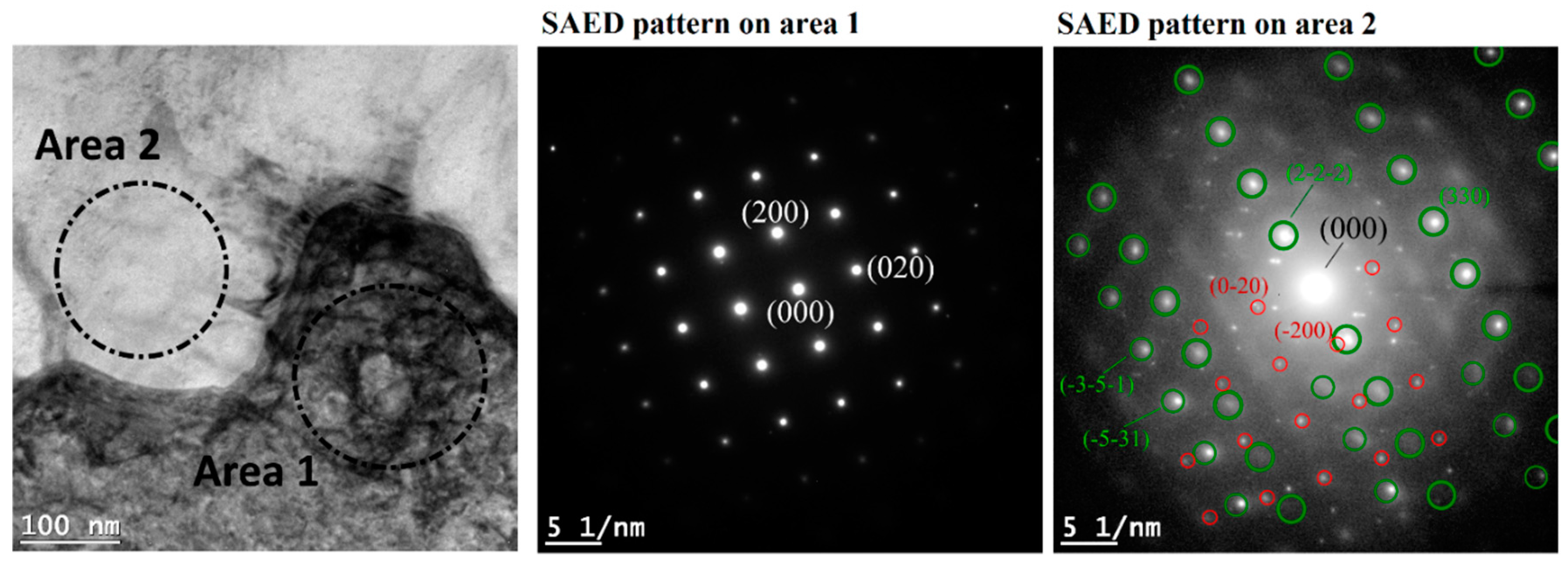
4.3. Formation of the Dendrite’s Features: Microsegregation, Eutectic Phases, and Dislocations
4.4. Evolution of the Microstructure during the Aging Treatment
5. Conclusions
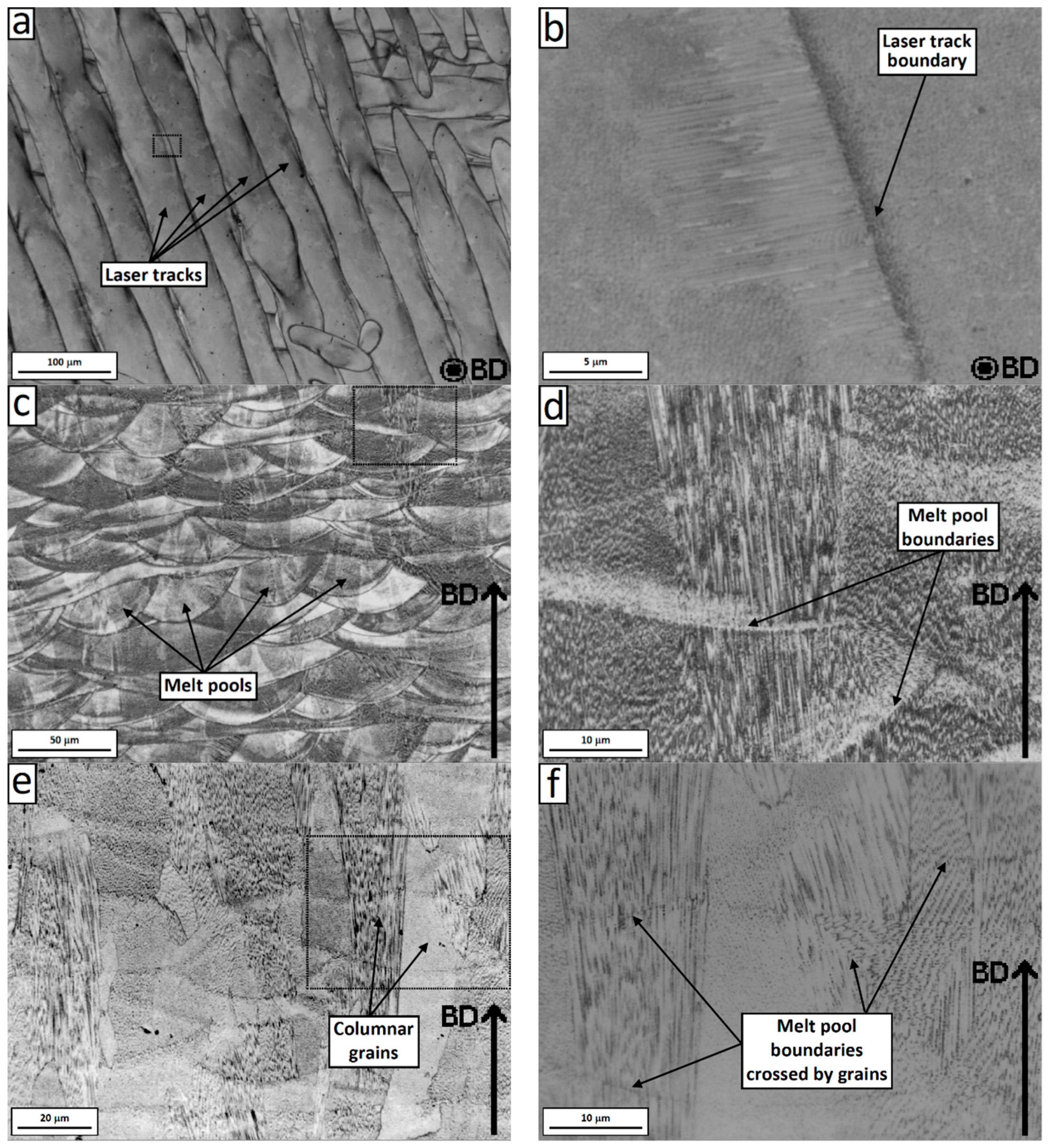
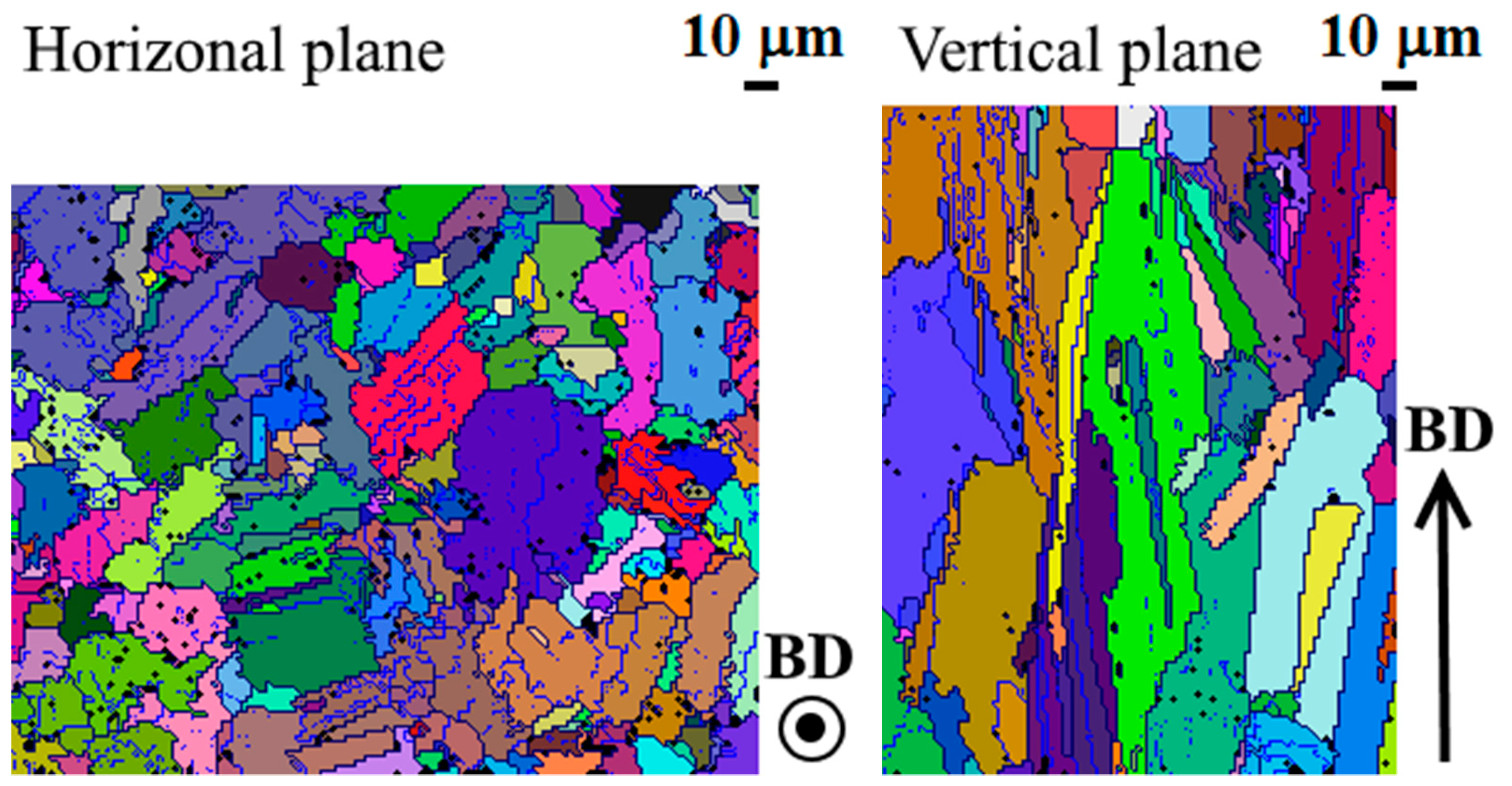
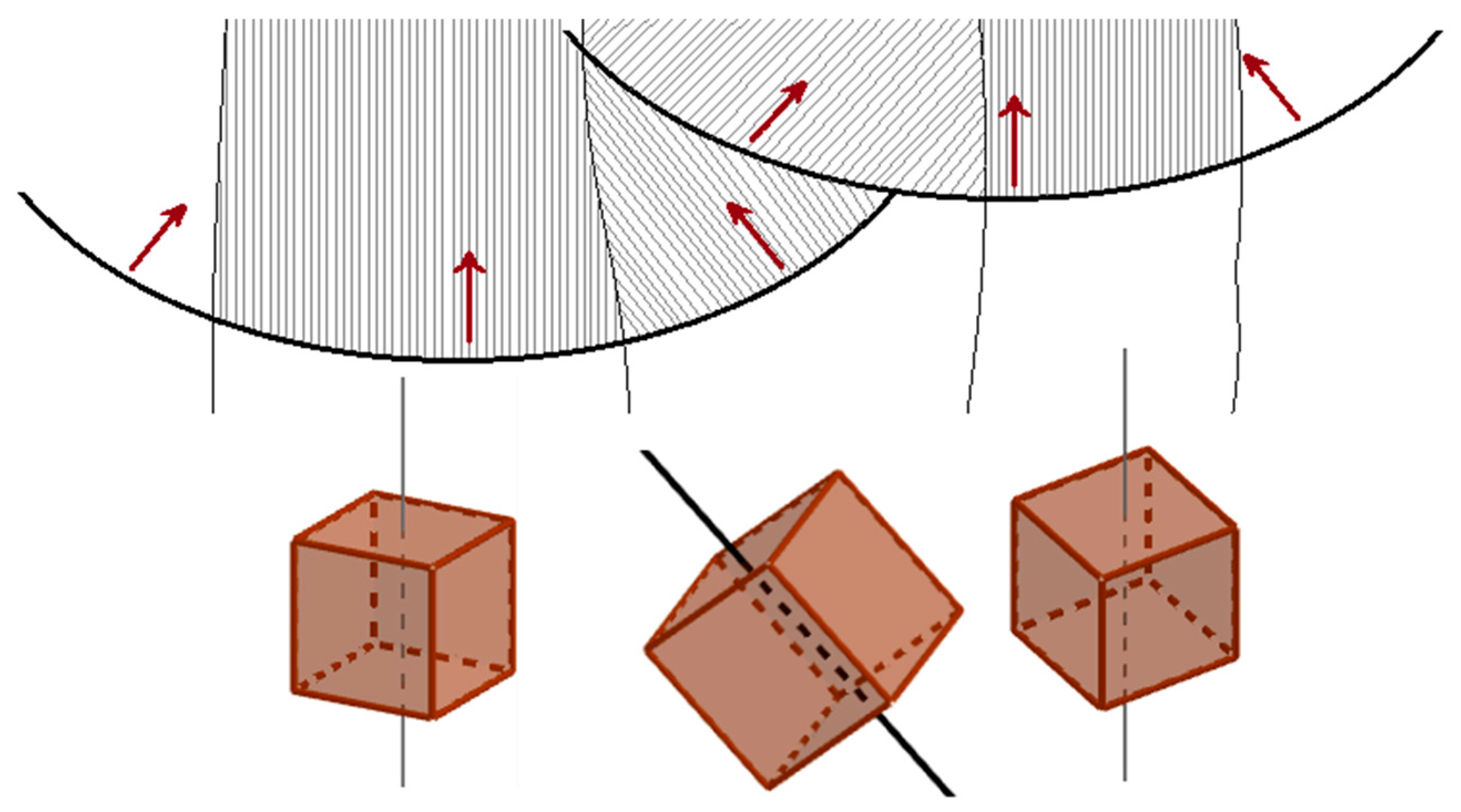
- Length scale from 10−3 to 10−4 m: Laser related features, columnar grains developed mainly along the build direction and not confined within the melt pools or laser tracks, and presence of subgranular domains separated by low-angle boundaries. The bimodal grain structure, which is usually reported when a periodic scanning strategy is adopted, was not observed in the current study. The 67° rotation scan strategy has a role in impeding the formation of the bimodal grain structure because it removes one constraint in the selection of the most favorably oriented grains; therefore, it is assumed to reduce harshness of the competitive growth and thus to favor epitaxial growth at the expense of heterogeneous nucleation;
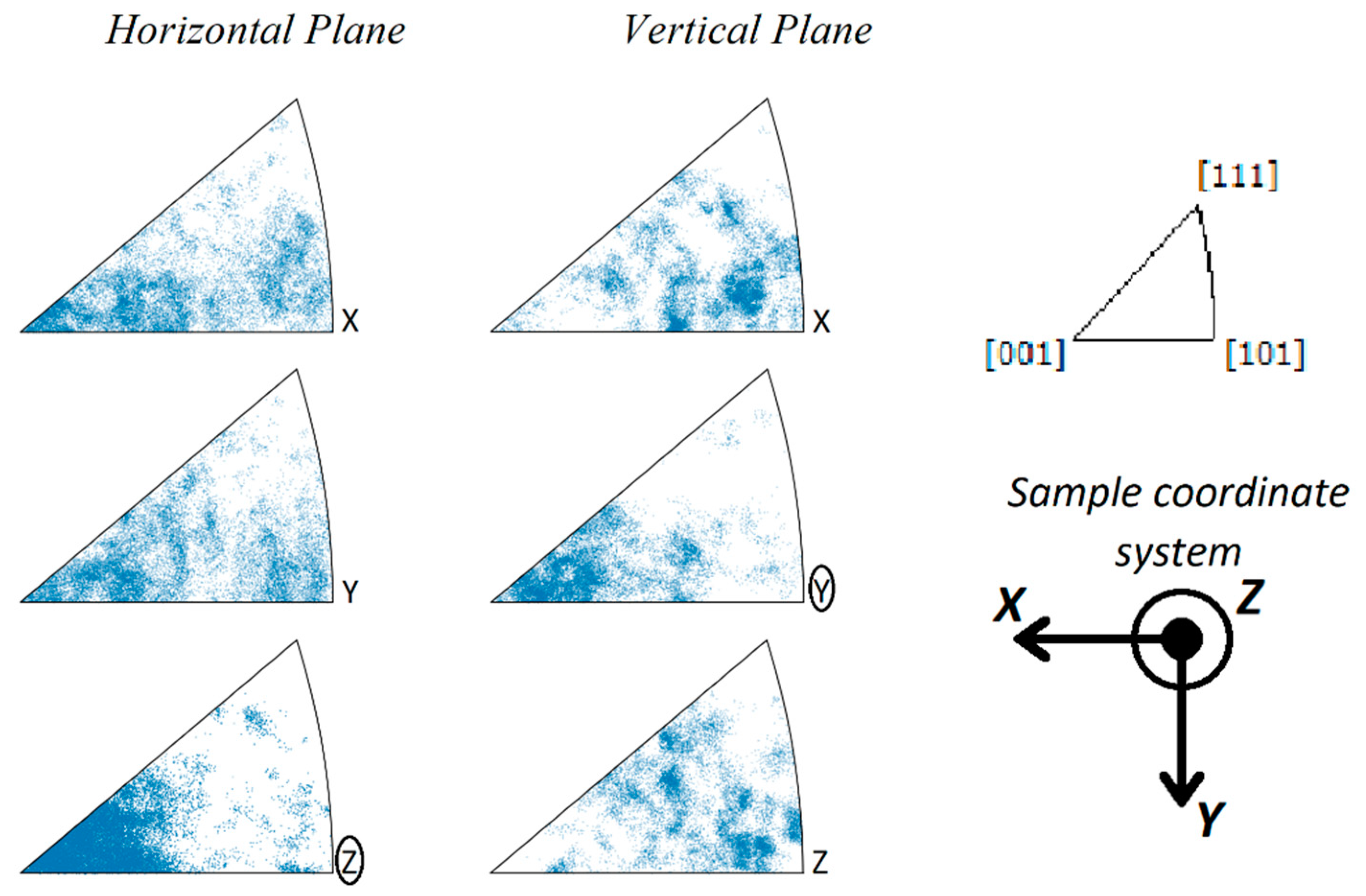
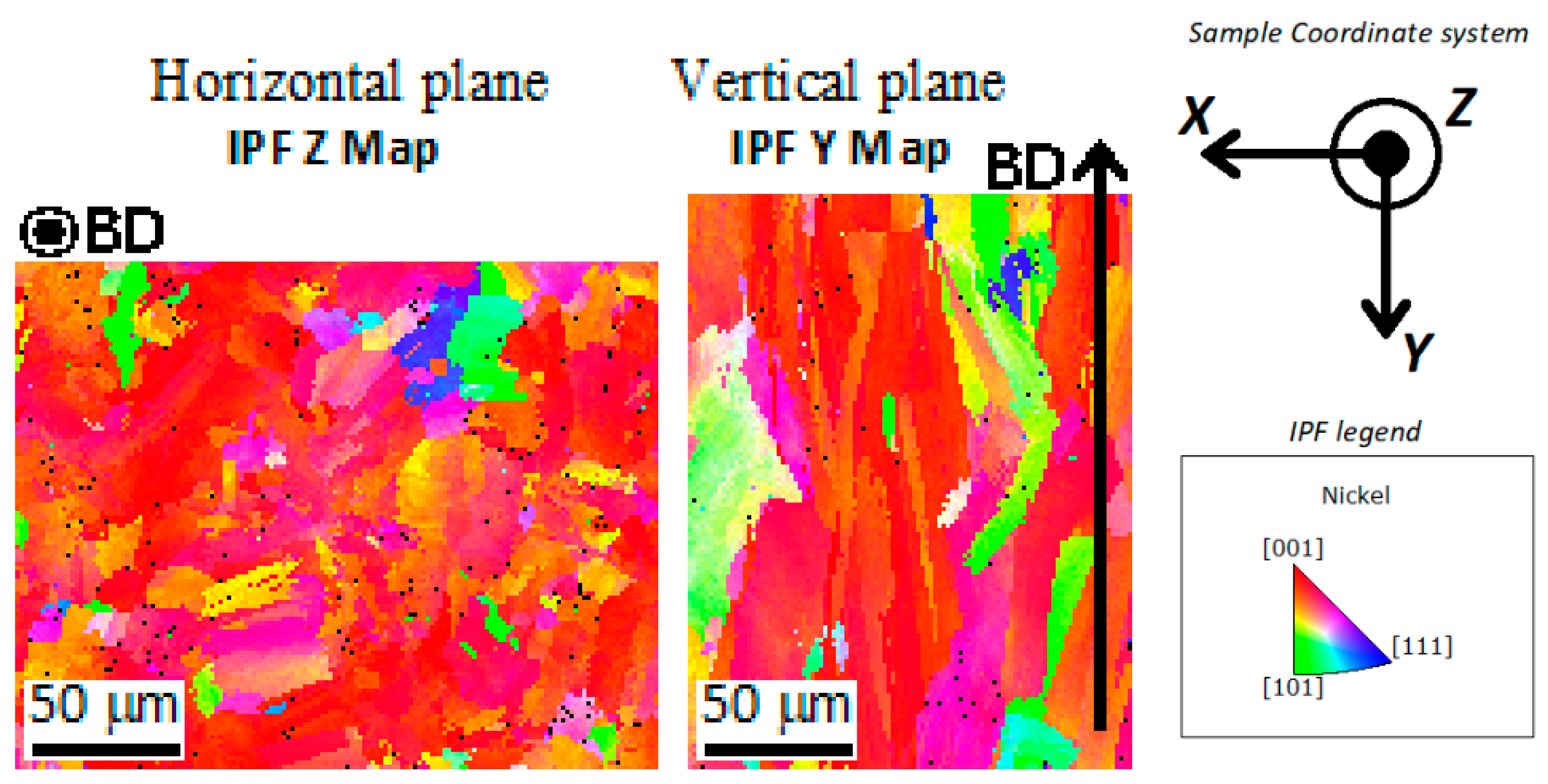
- Length scale from 10−4 to 10−5 m: Predominant <100> crystallographic texture of the grains and substantial isotropy of the crystallographic orientation around the build direction. The lack of observable texture on the horizontal plane is further evidence of the less severe selection of the growing grains;
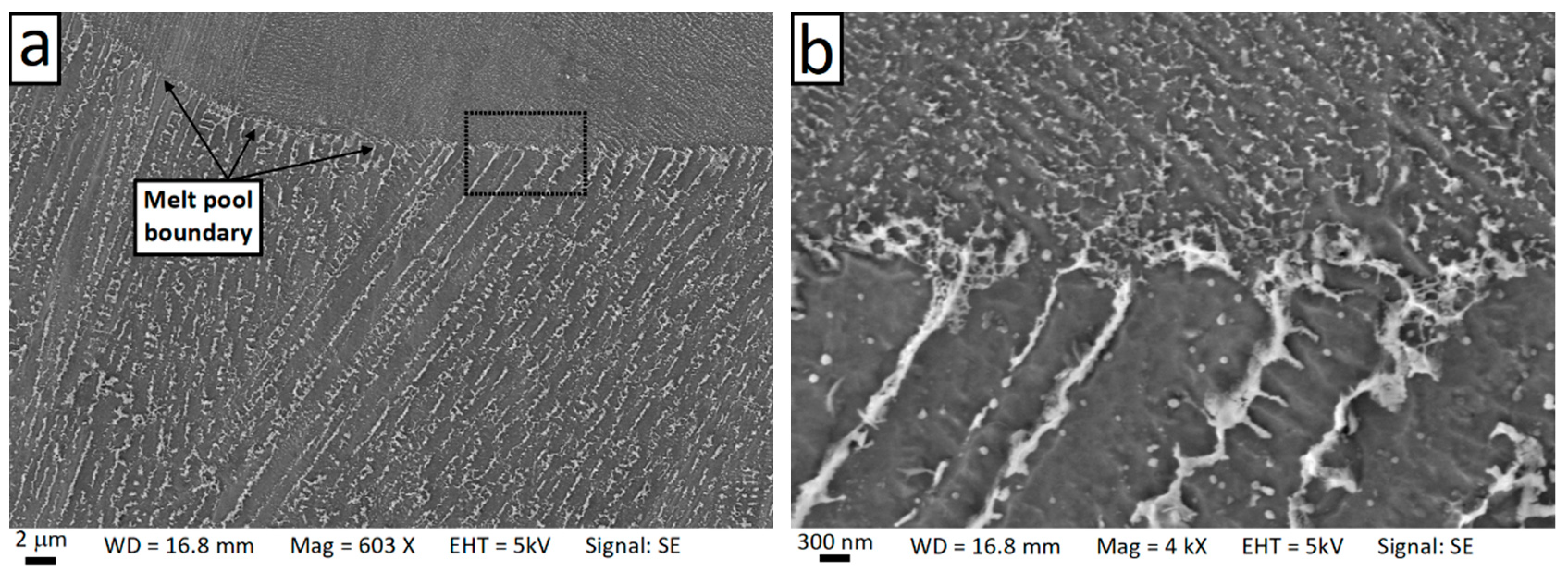
- Length scale from 10−5 to 10−6 m: Columnar intragranular dendrites mainly oriented along the build direction or grown following a zig-zag path along the melt pools due to abrupt changes of 90° in the growth direction. Contrary to what was found at the grain length scale, the microstructure at the length scale of dendrites was affected by the laser related boundaries, with abrupt changes in growth direction and dendrite size observed due to the nonuniform solidification conditions and the complex thermal field in the melt pool;
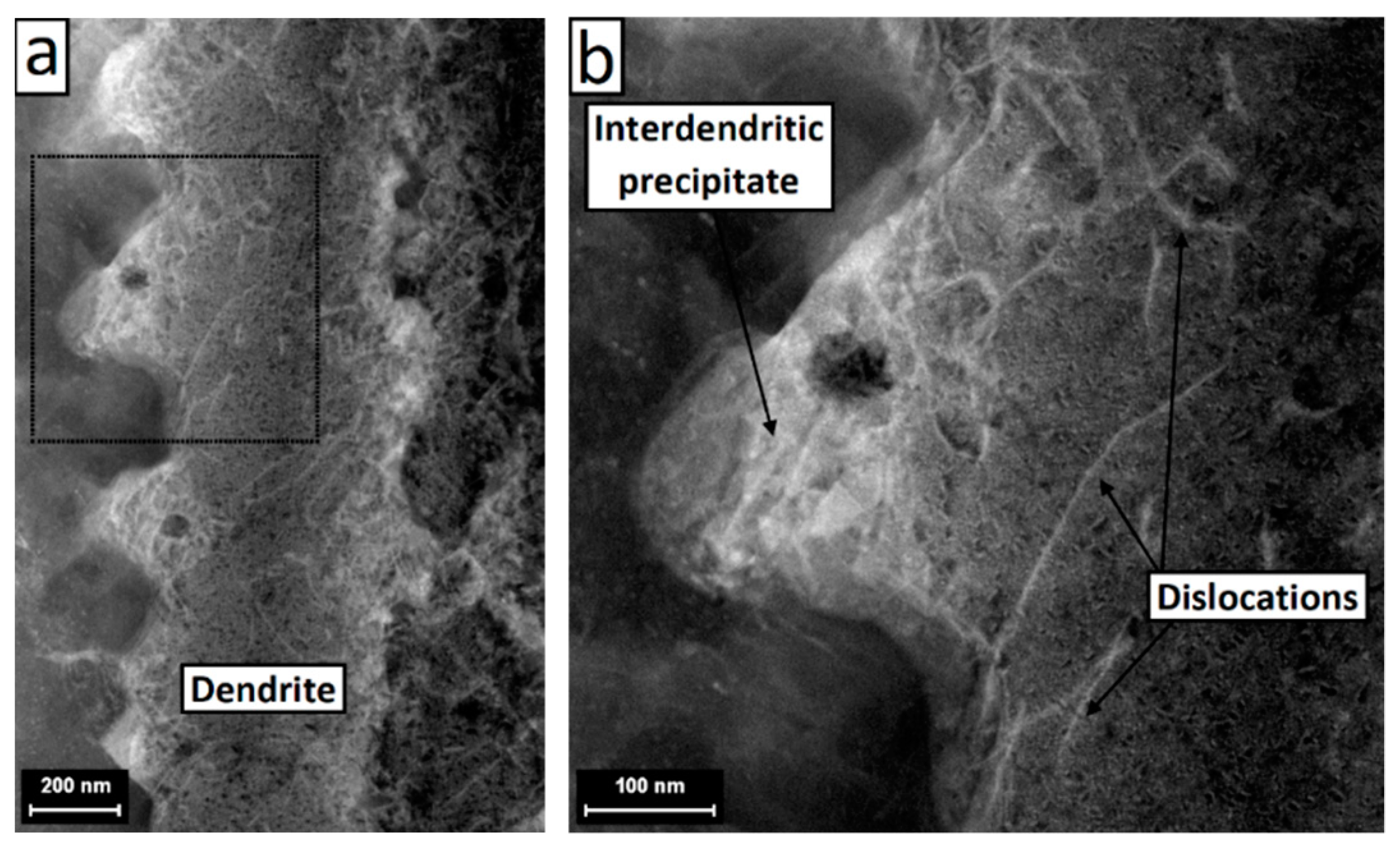
- Length scale from 10−6 to 10−8 m: Microsegregation of the alloying elements inside the dendrite and presence of extremely fine particles (i.e., carbides and Laves phases) and dislocations at the interdendric boundaries.
Author Contributions
Funding
Acknowledgments
Conflicts of Interest
References
- Thomas, A.; El-Wahabi, M.; Cabrera, J.M.; Prado, J.M. High temperature deformation of Inconel 718. J. Mater. Process. Technol. 2006, 177, 469–472. [Google Scholar] [CrossRef]
- Pieraggi, B.; Uginet, J.F. Fatigue and Creep Properties in Relation with Alloy 718 Microstructure. Superalloys 1994, 718, 625–706. [Google Scholar] [CrossRef]
- Greene, G.A.; Finfrock, C.C. Oxidation of Inconel 718 in Air at High Temperatures. Oxid. Met. 2001, 55, 505–521. [Google Scholar] [CrossRef]
- Al-Hatab, K.A.; Al-Bukhaiti, M.A.; Krupp, U.; Kantehm, M. Cyclic oxidation behavior of in 718 superalloy in air at high temperatures. Oxid. Met. 2011, 75, 209–228. [Google Scholar] [CrossRef]
- Akca, E.; Gürsel, A. A Review on Superalloys and IN718 Nickel-Based INCONEL Superalloy. Period. Eng. Nat. Sci. 2015, 3, 15–27. [Google Scholar] [CrossRef]
- Barker, J.F. The Initial Years of Alloy 718–A GE Perspective. Superalloy 718-Metall. Appl. 1989, 269–277. [Google Scholar] [CrossRef]
- Paulonis, D.F.; Schirra, J.J. Alloy 718 at Pratt & Whitney-Historical Perspective and Future Challenges. Superalloys 2001, 718, 13–23. [Google Scholar] [CrossRef]
- INCONEL Alloy 718. In Special Metals Company, Publication Number SMC-045. 2007. Available online: http://www.specialmetals.com/assets/smc/documents/inconel_alloy_718.pdf (accessed on 14 March 2019).
- Cozar, R.; Pineau, A. Morphology of Y′ and Y″ precipitates and thermal stability of Inconel 718 type alloys. Metall. Trans. 1973, 4, 47–59. [Google Scholar] [CrossRef]
- Radavich, J.F. The Physical Metallurgy of Cast and Wrought Alloy 718. Superalloys 1989, 718, 229–240. [Google Scholar] [CrossRef]
- Lingenfelter, A. Welding of Inconel Alloy 718: A Historical Overview. Superalloys 1989, 718, 673–683. [Google Scholar] [CrossRef]
- DuPont, J.N.; Lippold, J.C.; Kiser, S.D. Welding Metallurgy and Weldability of Nickel-Base Alloys, 1st ed.; John Wiley & Sons, Inc.: Hoboken, NJ, USA, 2009; ISBN 978-0-470-08714-5. [Google Scholar]
- Radhakrishna, C.; Rao, K.P. The formation and control of Laves phase in superalloy 718 welds. J. Mater. Sci. 1997, 32, 1977–1984. [Google Scholar] [CrossRef]
- Carter, L.N.; Attallah, M.M.; Reed, R.C. Laser Powder Bed Fabrication of Nickel-Base Superalloys: Influence of Parameters; Characterisation, Quantification and Mitigation of Cracking. In Proceedings of the Superalloys 2012: 12th International Symposium on Superalloys, Champion, PA, USA, 9–13 September 2012; Huron, E.S., Reed, R.C., Hardy, M.C., Mills, M.J., Montero, R.E., Portella, P.D., Telesman, J., Eds.; The Minerals, Metals & Materials Society: Pittsburgh, PA, USA; pp. 577–586. [Google Scholar] [CrossRef]
- Murr, L.E. Metallurgy of additive manufacturing: Examples from electron beam melting. Addit. Manuf. 2015, 5, 40–53. [Google Scholar] [CrossRef]
- Jia, Q.; Gu, D. Selective laser melting additive manufacturing of Inconel 718 superalloy parts: Densification, microstructure and properties. J. Alloy. Compd. 2014, 585, 713–721. [Google Scholar] [CrossRef]
- Kuo, Y.L.; Horikawa, S.; Kakehi, K. The effect of interdendritic δ phase on the mechanical properties of Alloy 718 built up by additive manufacturing. Mater. Des. 2017, 116, 411–418. [Google Scholar] [CrossRef]
- Gong, X.; Chou, K. Microstructures of Inconel 718 by Selective Laser Melting. In Proceedings of the TMS 2015 144th Annual Meeting & Exhibition, Orlando, FL, USA, 15–19 March 2015; The Minerals, Metals & Materials Society: Pittsburgh, PA, USA; pp. 461–468. [Google Scholar] [CrossRef]
- Amato, K.N.; Gaytan, S.M.; Murr, L.E.; Martinez, E.; Shindo, P.W.; Hernandez, J.; Collins, S.; Medina, F. Microstructures and mechanical behavior of Inconel 718 fabricated by selective laser melting. Acta Mater. 2012, 60, 2229–2239. [Google Scholar] [CrossRef]
- Wang, Z.; Guan, K.; Gao, M.; Li, X.; Chen, X.; Zeng, X. The microstructure and mechanical properties of deposited-IN718 by selective laser melting. J. Alloy. Compd. 2012, 513, 518–523. [Google Scholar] [CrossRef]
- DebRoy, T.; Wei, H.L.; Zuback, J.S.; Mukherjee, T.; Elmer, J.W.; Milewski, J.O.; Beese, A.M.; Wilson-Heid, A.; De, A.; Zhang, W. Additive manufacturing of metallic components–Process, structure and properties. Prog. Mater. Sci. 2018, 92, 112–224. [Google Scholar] [CrossRef]
- Murr, L.E.; Martinez, E.; Amato, K.N.; Gaytan, S.M.; Hernandez, J.; Ramirez, D.A.; Shindo, P.W.; Medina, F.; Wicker, R.B. Fabrication of metal and alloy components by additive manufacturing: Examples of 3D materials science. J. Mater. Res. Technol. 2012, 1, 42–54. [Google Scholar] [CrossRef]
- Simchi, A. Direct laser sintering of metal powders: Mechanism, kinetics and microstructural features. Mater. Sci. Eng. A 2006, 428, 148–158. [Google Scholar] [CrossRef]
- Yap, C.Y.; Chua, C.K.; Dong, Z.L.; Liu, Z.H.; Zhang, D.Q.; Loh, L.E.; Sing, S.L. Review of selective laser melting: Materials and applications. Appl. Phys. Rev. 2015, 2, 1–21. [Google Scholar] [CrossRef]
- Zhang, D.; Niu, W.; Cao, X.; Liu, Z. Effect of standard heat treatment on the microstructure and mechanical properties of selective laser melting manufactured Inconel 718 superalloy. Mater. Sci. Eng. A 2015, 644, 32–40. [Google Scholar] [CrossRef]
- Qi, H.; Azer, M.; Ritter, A. Studies of Standard Heat Treatment Effects on Microstructure and Mechanical Properties of Laser Net Shape Manufactured INCONEL 718. Metall. Mater. Trans. A 2009, 40, 2410–2422. [Google Scholar] [CrossRef]
- Maamoun, A.H.; Xue, Y.F.; Elbestawi, M.A.; Veldhuis, S.C. The Effect of Selective Laser Melting Process Parameters on the Microstructure and Mechanical Properties of Al6061 and AlSi10Mg Alloys. Materials 2019, 12, 12. [Google Scholar] [CrossRef]
- Uzan, N.E.; Shneck, R.; Yeheskel, O.; Frage, N. Fatigue of AlSi10Mg specimens fabricated by additive manufacturing selective laser melting (AM-SLM). Mater. Sci. Eng. A 2017, 704, 229–237. [Google Scholar] [CrossRef]
- Qiu, C.; Adkins, N.J.E.; Attallah, M.M. Microstructure and tensile properties of selectively laser-melted and of HIPed laser-melted Ti-6Al-4V. Mater. Sci. Eng. A 2013, 578, 230–239. [Google Scholar] [CrossRef]
- Divya, V.D.; Muñoz-Moreno, R.; Messé, O.M.D.M.; Barnard, J.S.; Baker, S.; Illston, T.; Stone, H.J. Microstructure of selective laser melted CM247LC nickel-based superalloy and its evolution through heat treatment. Mater. Charact. 2016, 114, 62–74. [Google Scholar] [CrossRef]
- Kanagarajah, P.; Brenne, F.; Niendorf, T.; Maier, H.J. Inconel 939 processed by selective laser melting: Effect of microstructure and temperature on the mechanical properties under static and cyclic loading. Mater. Sci. Eng. A 2013, 588, 188–195. [Google Scholar] [CrossRef]
- Roberts, I.A.; Wang, C.J.; Esterlein, R.; Stanford, M.; Mynors, D.J. A three-dimensional finite element analysis of the temperature field during laser melting of metal powders in additive layer manufacturing. Int. J. Mach. Tools Manuf. 2009, 49, 916–923. [Google Scholar] [CrossRef]
- Tian, Y.; McAllister, D.; Colijn, H.; Mills, M.; Farson, D.; Nordin, M.; Babu, S. Rationalization of microstructure heterogeneity in INCONEL 718 builds made by the direct laser additive manufacturing process. Metall. Mater. Trans. A 2014, 45, 4470–4483. [Google Scholar] [CrossRef]
- Wang, X.; Chou, K. Effects of thermal cycles on the microstructure evolution of Inconel 718 during selective laser melting process. Addit. Manuf. 2017, 18, 1–14. [Google Scholar] [CrossRef]
- Popovich, V.A.; Borisov, E.V.; Popovich, A.A.; Sufiiarov, V.S.; Masaylo, D.V.; Alzina, L. Functionally graded Inconel 718 processed by additive manufacturing: Crystallographic texture, anisotropy of microstructure and mechanical properties. Mater. Des. 2017, 114, 441–449. [Google Scholar] [CrossRef]
- Mostafa, A.; Rubio, I.P.; Brailovski, V.; Jahazi, M.; Medraj, M. Structure, Texture and Phases in 3D Printed IN718 Alloy Subjected to Homogenization and HIP Treatments. Metals 2017, 7, 196. [Google Scholar] [CrossRef]
- Dinda, G.P.; Dasgupta, A.K.; Mazumder, J. Texture control during laser deposition of nickel-based superalloy. Scr. Mater. 2012, 67, 503–506. [Google Scholar] [CrossRef]
- Chlebus, E.; Gruber, K.; Kuźnicka, B.; Kurzac, J.; Kurzynowski, T. Effect of heat treatment on microstructure and mechanical properties of Inconel 718 processed by selective laser melting. Mater. Sci. Eng. A 2015, 639, 647–655. [Google Scholar] [CrossRef]
- Smith, D.H.; Bicknell, J.; Jorgensen, L.; Patterson, B.M.; Cordes, N.L.; Tsukrov, I.; Knezevic, M. Microstructure and mechanical behavior of direct metal laser sintered Inconel alloy 718. Mater. Charact. 2016, 113, 1–9. [Google Scholar] [CrossRef]
- Popovich, V.A.; Borisov, E.V.; Popovich, A.A.; Sufiiarov, V.S.; Masaylo, D.V.; Alzina, L. Impact of heat treatment on mechanical behaviour of Inconel 718 processed with tailored microstructure by selective laser melting. Mater. Des. 2017, 131, 12–22. [Google Scholar] [CrossRef]
- Li, J.; Zhao, Z.; Bai, P.; Qu, H.; Liu, B.; Li, L.; Wu, L.; Guan, R.; Liu, H.; Guo, Z. Microstructural evolution and mechanical properties of IN718 alloy fabricated by selective laser melting following different heat treatments. J. Alloy. Compd. 2019, 772, 861–870. [Google Scholar] [CrossRef]
- Holland, S.; Wang, X.; Chen, J.; Cai, W.; Yan, F.; Li, L. Multiscale characterization of microstructures and mechanical properties of Inconel 718 fabricated by selective laser melting. J. Alloy. Compd. 2019, 784, 182–194. [Google Scholar] [CrossRef]
- Calandri, M.; Manfredi, D.; Calignano, F.; Ambrosio, E.P.; Biamino, S.; Lupoi, R.; Ugues, D. Solution Treatment Study of Inconel 718 Produced by SLM Additive Technique in View of the Oxidation Resistance. Adv. Eng. Mater. 2018, 20, 1800351. [Google Scholar] [CrossRef]
- EOS NickelAlloy IN718, In EOS Electro Optical System: Industrial 3D Printing, Material Data Sheet. 2014. Available online: http://ip-saas-eos-cms.s3.amazonaws.com/public/4528b4a1bf688496/ff974161c2057e6df56db5b67f0f5595/EOS_NickelAlloy_IN718_en.pdf (accessed on 14 March 2019).
- ASTM B962-17, Standard Test Methods for Density of Compacted or Sintered Powder Metallurgy (PM) Products Using Archimedes’ Principle; Astm International: West Conshohocken, PA, USA, 2017.
- Bassini, E.; Calandri, M.; Parizia, S.; Marchese, G.; Biamino, S.; Ugues, D. Ottimizzazione dei parametri di processo e cenni sui trattamenti termici per la realizzazione di componenti in Inconel 625 e 718 via Selective Laser Melting (SLM). In Proceedings of the 37° Convegno Nazionale AIM, Bologna, Italy, 12–14 September 2018. [Google Scholar]
- Shifeng, W.; Shuai, L.; Qingsong, W.; Yan, C.; Sheng, Z.; Yusheng, S. Effect of molten pool boundaries on the mechanical properties of selective laser melting parts. J. Mater. Process. Technol. 2014, 214, 2660–2667. [Google Scholar] [CrossRef]
- Krakow, R.; Johnstone, D.N.; Eggeman, A.S.; Hünert, D.; Hardy, M.C.; Rae, C.M.F.; Midgley, P.A. On the crystallography and composition of topologically close-packed phases in ATI 718Plus®. Acta Mater. 2017, 130, 271–280. [Google Scholar] [CrossRef]
- Manikandan, S.G.K.; Sivakumar, D.; Rao, K.P.; Kamaraj, M. Laves phase in alloy 718 fusion zone-microscopic and calorimetric studies. Mater. Charact. 2015, 100, 192–206. [Google Scholar] [CrossRef]
- Brenne, F.; Taube, A.; Pröbstle, M.; Neumeier, S.; Schwarze, D.; Schaper, M.; Niendorf, T. Microstructural design of Ni-base alloys for high-temperature applications: Impact of heat treatment on microstructure and mechanical properties after selective laser melting. Prog. Addit. Manuf. 2016, 1, 141–151. [Google Scholar] [CrossRef]
- Cao, G.H.; Sun, T.Y.; Wang, C.H.; Li, X.; Liu, M.; Zhang, Z.X.; Hu, P.F.; Russell, A.M.; Schneider, R.; Gerthsen, D.; et al. Investigations of γ′, γ″ and δ precipitates in heat-treated Inconel 718 alloy fabricated by selective laser melting. Mater. Charact. 2018, 136, 398–406. [Google Scholar] [CrossRef]
- Zhang, F.; Levine, L.E.; Allen, A.J.; Stoudt, M.R.; Lindwall, G.; Lass, E.A.; Williams, M.E.; Idell, Y.; Campbell, C.E. Effect of heat treatment on the microstructural evolution of a nickel- based superalloy additive-manufactured by laser powder bed fusion. Acta Mater. 2018, 152, 200–214. [Google Scholar] [CrossRef]
- Tucho, W.M.; Cuvillier, P.; Sjolyst-Kverneland, A.; Hansen, V. Microstructure and hardness studies of Inconel 718 manufactured by selective laser melting before and after solution heat treatment. Mater. Sci. Eng. A 2017, 689, 220–232. [Google Scholar] [CrossRef]
- Yan, Z.; Liu, W.; Tang, Z.; Liu, X.; Zhang, N.; Li, M.; Zhang, H. Review on thermal analysis in laser-based additive manufacturing. Opt. Laser Technol. 2018, 106, 427–441. [Google Scholar] [CrossRef]
- Kou, S. Welding Metallurgy, 2nd ed.; Chapman & Hall: London, UK, 2003; ISBN 0-471-43491-4. [Google Scholar]
- Liu, F.; Lin, X.; Huang, C.; Song, M.; Yang, G.; Chen, J.; Huang, W. The effect of laser scanning path on microstructures and mechanical properties of laser solid formed nickel-base superalloy Inconel 718. J. Alloy. Compd. 2011, 509, 4505–4509. [Google Scholar] [CrossRef]
- Kuo, Y.-L.; Horikawa, S.; Kakehi, K. Effects of build direction and heat treatment on creep properties of Ni-base superalloy built up by additive manufacturing. Scr. Mater. 2017, 129, 74–78. [Google Scholar] [CrossRef]
- Porter, D.A.; Easterling, K.E. Phase Transformations in Metals and Alloys, 2nd ed.; Chapman & Hall: London, UK, 1992; ISBN 978-1-4899-3051-4. [Google Scholar]
- Xia, M.; Gu, D.; Yu, G.; Dai, D.; Chen, H.; Shi, Q. Selective laser melting 3D printing of Ni-based superalloy: Understanding thermodynamic mechanisms. Sci. Bull. 2016, 61, 1013–1022. [Google Scholar] [CrossRef]
- Acharya, R.; Sharon, J.A.; Staroselsky, A. Prediction of microstructure in laser powder bed fusion process. Acta Mater. 2017, 124, 360–371. [Google Scholar] [CrossRef]
- Wei, H.L.; Mazumder, J.; DebRoy, T. Evolution of solidification texture during additive manufacturing. Sci. Rep. 2015, 5, 1–7. [Google Scholar] [CrossRef] [PubMed]
- Wei, H.L.; Elmer, J.W.; Debroy, T. Origin of grain orientation during solidification of an aluminum alloy. Acta Mater. 2016, 115, 123–131. [Google Scholar] [CrossRef]
- Wan, H.Y.; Zhou, Z.J.; Li, C.P.; Chen, G.F.; Zhang, G.P. Effect of scanning strategy on grain structure and crystallographic texture of Inconel 718 processed by selective laser melting. J. Mater. Sci. Technol. 2018, 34, 1799–1804. [Google Scholar] [CrossRef]
- Choi, J.P.; Shin, G.H.; Yang, S.; Yang, D.Y.; Lee, J.S.; Brochu, M.; Yu, J.H. Densification and microstructural investigation of Inconel 718 parts fabricated by selective laser melting. Powder Technol. 2017, 310, 60–66. [Google Scholar] [CrossRef]
- Wang, X.; Chou, K. Electron Backscatter Diffraction Analysis of Inconel 718 Parts Fabricated by Selective Laser Melting Additive Manufacturing. JOM 2017, 69, 402–408. [Google Scholar] [CrossRef]
- Carter, L.N.; Martin, C.; Withers, P.J.; Attallah, M.M. The influence of the laser scan strategy on grain structure and cracking behaviour in SLM powder-bed fabricated nickel superalloy. J. Alloy. Compd. 2014, 615, 338–347. [Google Scholar] [CrossRef]
- Thijs, L.; Sistiaga, M.L.M.; Wauthle, R.; Xie, Q.; Kruth, J.-P.; Van Humbeeck, J. Strong morphological and crystallographic texture and resulting yield strength anisotropy in selective laser melted tantalum. Acta Mater. 2013, 61, 4657–4668. [Google Scholar] [CrossRef]
- Lee, J.S.; Gu, J.H.; Jung, H.M.; Kim, E.H.; Jung, Y.G.; Lee, J.H. Directional solidification microstructure control in CM247LC superalloy. Mater. Today Proc. 2014, 1, 3–10. [Google Scholar] [CrossRef]
- Stefanescu, D.M.; Ruxanda, R. Fundamentals of Solidification. In ASM Handbook, Metallography and Microstructures; Vander Voort, G.F., Ed.; ASM International: Materials Park, OH, USA, 2004; Volume 9, pp. 71–92. ISBN 978-0-87170-706-2. [Google Scholar]
- Hooper, P.A. Melt pool temperature and cooling rates in laser powder bed fusion. Addit. Manuf. 2018, 22, 548–559. [Google Scholar] [CrossRef]
- Li, S.; Xiao, H.; Liu, K.; Xiao, W.; Li, Y.; Han, X.; Mazumder, J.; Song, L. Melt-pool motion, temperature variation and dendritic morphology of Inconel 718 during pulsed- and continuous-wave laser additive manufacturing: A comparative study. Mater. Des. 2017, 119, 351–360. [Google Scholar] [CrossRef]
- Song, J.; Chew, Y.; Bi, G.; Yao, X.; Zhang, B.; Bai, J.; Moon, S.K. Numerical and experimental study of laser aided additive manufacturing for melt-pool profile and grain orientation analysis. Mater. Des. 2018, 137, 286–297. [Google Scholar] [CrossRef]
- Ali, H.; Ghadbeigi, H.; Mumtaz, K. Effect of scanning strategies on residual stress and mechanical properties of Selective Laser Melted Ti6Al4V. Mater. Sci. Eng. A 2018, 712, 175–187. [Google Scholar] [CrossRef]
- Parimi, L.L.; Ravi, G.; Clark, D.; Attallah, M.M. Microstructural and texture development in direct laser fabricated IN718. Mater. Charact. 2014, 89, 102–111. [Google Scholar] [CrossRef]
- Deng, D.; Peng, R.L.; Brodin, H.; Moverare, J. Microstructure and mechanical properties of Inconel 718 produced by selective laser melting: Sample orientation dependence and effects of post heat treatments. Mater. Sci. Eng. A 2018, 713, 294–306. [Google Scholar] [CrossRef]
- Kang, S.-H.; Deguchi, Y.; Yamamoto, K.; Ogi, K.; Shirai, M. Solidification Process and Behavior of Alloying Elements in Ni-Based Superalloy Inconel718. Mater. Trans. 2004, 45, 2728–2733. [Google Scholar] [CrossRef][Green Version]
- Knorovsky, G.A.; Cieslak, M.J.; Headley, T.J.; Romig, A.D.; Hammetter, W.F. INCONEL 718: A Solidification Diagram. Metall. Trans. A 1989, 20, 2149–2158. [Google Scholar] [CrossRef]
- DuPont, J.N.; Robino, C.V.; Michael, J.R.; Notis, M.R.; Marder, A.R. Solidification of Nb-Bearing Superalloys: Part, I. Reaction Sequences. Metall. Mater. Trans. A 1998, 29, 2785–2796. [Google Scholar] [CrossRef]
- DuPont, J.N.; Robino, C.V.; Marder, A.R.; Notis, M.R. Solidification of Nb-bearing superalloys: Part II. Pseudoternary solidification surfaces. Metall. Mater. Trans. A 1998, 29, 2797–2806. [Google Scholar] [CrossRef]
- Dupont, J.N.; Robino, C.V.; Marder, A.R. Modeling solute redistribution and microstructural development in fusion welds of Nb-bearing superalloys. Acta Mater. 1998, 46, 4781–4790. [Google Scholar] [CrossRef]
- Wilson, A.S. Formation and effect of topologically close-packed phases in nickel-base superalloys. Mater. Sci. Technol. 2017, 33, 1108–1118. [Google Scholar] [CrossRef]
- Schirra, J.J.; Caless, R.H.; Hatala, R.W. The effect of laves phases on the mechanical properties of wrought and cast + HIP Inconel 718. Superalloys 1991, 718, 375–388. [Google Scholar] [CrossRef]
- Slama, C.; Abdellaoui, M. Structural characterization of the aged Inconel 718. J. Alloy. Compd. 2000, 306, 277–284. [Google Scholar] [CrossRef]
- Rao, G.A.; Kumar, M.; Srinivas, M.; Sarma, D.S. Effect of standard heat treatment on the microstructure and mechanical properties of hot isostatically pressed superalloy inconel 718. Mater. Sci. Eng. A 2003, 355, 114–125. [Google Scholar] [CrossRef]
- Sundararaman, M.; Mukhopadhyay, P.; Banerjee, S. Precipitation and Room Temperature Deformation Behaviour of Inconel 718. Superalloys 1994, 718, 419–440. [Google Scholar] [CrossRef]
- Azadian, S.; Wei, L.Y.; Warren, R. Delta phase precipitation in Inconel 718. Mater. Charact. 2004, 53, 7–16. [Google Scholar] [CrossRef]
- Anderson, M.; Thielin, A.-L.; Bridier, F.; Bocher, P.; Savoie, J. Phase precipitation in Inconel 718 and associated mechanical properties. Mater. Sci. Eng. A 2017, 679, 48–55. [Google Scholar] [CrossRef]
- Slama, C.; Servant, C.; Cizeron, G. Aging of the Inconel 718 alloys between 500 and 750 °C. J. Mater. Res. 1997, 12, 2298–2316. [Google Scholar] [CrossRef]
- Sjoberg, G.; Ingesten, N.-G.; Carlson, R.G. Grain Boundary delta-phase Morphologies, Carbides and Notch Rupture Sensitivity of Cast Alloy 718. Superalloys 1991, 718, 603–620. [Google Scholar] [CrossRef]
- Nunes, R.M.; Pereira, D.; Clarke, T.; Hirsch, T.K. Delta Phase Characterization in Inconel 718 Alloys Through X-ray Diffraction. ISIJ Int. 2015, 55, 2450–2454. [Google Scholar] [CrossRef]
- Rong, Y.; Chen, S.; Gengxiang, H.U.; Gao, M.; Wei, R.P. Prediction and characterization of variant electron diffraction patterns for γ″ and δ precipitates in an INCONEL 718 alloy. Metall. Mater. Trans. A 1999, 30, 2297–2303. [Google Scholar] [CrossRef]


| Ni | Cr | Nb | Mo | Ti | Al | Fe |
| 50–55 | 17–21 | 4.75–5.5 | 2.8–3.3 | 0.65–1.15 | 0.2–0.8 | balance |
| Co | Cu | C | Si + Mn | P + S | B | |
| <1 | <0.3 | <0.08 | <0.35 | <0.015 | <0.006 |
| Sample | Power [W] | Scan Speed [mm/s] | Hatching Distance [mm] | VED [J/mm3] |
|---|---|---|---|---|
| 1 | 175 | 600 | 0.09 | 162.04 |
| 2 | 195 | 600 | 0.09 | 180.56 |
| 3 | 175 | 900 | 0.07 | 138.89 |
| 4 | 175 | 1200 | 0.11 | 66.29 |
| 5 | 175 | 1200 | 0.07 | 104.17 |
| 6 | 185 | 600 | 0.09 | 171.30 |
| 7 | 185 | 1200 | 0.11 | 70.08 |
| 8 | 185 | 900 | 0.07 | 146.83 |
| 9 | 175 | 1200 | 0.09 | 81.02 |
| 10 | 185 | 900 | 0.11 | 93.43 |
| 11 | 195 | 900 | 0.07 | 154.76 |
| 12 | 185 | 600 | 0.07 | 220.24 |
| 13 | 195 | 600 | 0.07 | 232.14 |
| 14 | 195 | 1200 | 0.09 | 90.28 |
| 15 | 175 | 600 | 0.07 | 208.33 |
| 16 | 195 | 1200 | 0.11 | 73.86 |
| 17 | 195 | 900 | 0.09 | 120.37 |
| 18 | 185 | 900 | 0.09 | 114.20 |
| 19 | 185 | 1200 | 0.07 | 110.12 |
| 20 | 185 | 1200 | 0.09 | 85.65 |
| 21 | 175 | 900 | 0.09 | 108.02 |
| 22 | 175 | 600 | 0.11 | 132.58 |
| 23 | 195 | 600 | 0.11 | 147.73 |
| 24 | 195 | 1200 | 0.07 | 116.07 |
| 25 | 185 | 600 | 0.11 | 140.15 |
| 26 | 195 | 900 | 0.11 | 98.48 |
| 27 | 175 | 900 | 0.11 | 88.38 |
| Parameter | Value |
|---|---|
| Laser power (W) | 195 |
| Scan speed (mm/s) | 1200 |
| Hatching distance (mm) | 0.09 |
| Spot size (μm) | 100 |
| Layer thickness (μm) | 20 |
| Sample | Heat Treatment Recipe | Total Aging Exposure |
|---|---|---|
| Disk 1 | 1065 °C/2 h, 565 °C/4 h | 4 h |
| +565 °C/20 h | 24 h | |
| Disk 2 | 1065 °C/2h, 740 °C/2 h | 2 h |
| +740 °C/6 h | 8 h | |
| +740 °C/16 h | 24 h | |
| Disk 3 | 1065 °C/2 h, 800 °C/4 h | 4 h |
| +800 °C/20 h | 24 h | |
| Disk 4 | 1065 °C/2 h, 870 °C/4 h | 4 h |
| +870 °C/4 h | 8 h | |
| +870 °C/16 h | 24 h |
© 2019 by the authors. Licensee MDPI, Basel, Switzerland. This article is an open access article distributed under the terms and conditions of the Creative Commons Attribution (CC BY) license (http://creativecommons.org/licenses/by/4.0/).
Share and Cite
Calandri, M.; Yin, S.; Aldwell, B.; Calignano, F.; Lupoi, R.; Ugues, D. Texture and Microstructural Features at Different Length Scales in Inconel 718 Produced by Selective Laser Melting. Materials 2019, 12, 1293. https://doi.org/10.3390/ma12081293
Calandri M, Yin S, Aldwell B, Calignano F, Lupoi R, Ugues D. Texture and Microstructural Features at Different Length Scales in Inconel 718 Produced by Selective Laser Melting. Materials. 2019; 12(8):1293. https://doi.org/10.3390/ma12081293
Chicago/Turabian StyleCalandri, Michele, Shuo Yin, Barry Aldwell, Flaviana Calignano, Rocco Lupoi, and Daniele Ugues. 2019. "Texture and Microstructural Features at Different Length Scales in Inconel 718 Produced by Selective Laser Melting" Materials 12, no. 8: 1293. https://doi.org/10.3390/ma12081293
APA StyleCalandri, M., Yin, S., Aldwell, B., Calignano, F., Lupoi, R., & Ugues, D. (2019). Texture and Microstructural Features at Different Length Scales in Inconel 718 Produced by Selective Laser Melting. Materials, 12(8), 1293. https://doi.org/10.3390/ma12081293