Abstract
We report an excellent growth behavior of a high-κ dielectric on ReS2, a two-dimensional (2D) transition metal dichalcogenide (TMD). The atomic layer deposition (ALD) of an Al2O3 thin film on the UV-Ozone pretreated surface of ReS2 yields a pinhole free and conformal growth. In-situ half-cycle X-ray photoelectron spectroscopy (XPS) was used to monitor the interfacial chemistry and ex-situ atomic force microscopy (AFM) was used to evaluate the surface morphology. A significant enhancement in the uniformity of the Al2O3 thin film was deposited via plasma-enhanced atomic layer deposition (PEALD), while pinhole free Al2O3 was achieved using a UV-Ozone pretreatment. The ReS2 substrate stays intact during all different experiments and processes without any formation of the Re oxide. This work demonstrates that a combination of the ALD process and the formation of weak S–O bonds presents an effective route for a uniform and conformal high-κ dielectric for advanced devices based on 2D materials.
1. Introduction
Transition metal dichalcogenides (TMDs) have emerged as strong candidates to be implemented as the semiconductor channel in Field Effect Transistor (FET) applications [1,2]. Their remarkable properties, such as sizable electronic bandgaps and the capability to scale down to sub-nanometer thickness, make semiconducting TMDs ideal candidates for applications in nanoelectronics [3]. Most semiconducting TMDs show significant changes in electronic properties from the bulk to the monolayer form, such as an indirect to direct band gap crossover [4]. Such properties provide opportunities to engineer material heterostructures to fit specific device requirements.
The reports on ReS2 are relatively limited compared to other TMD materials. ReS2 crystallizes in a distorted 1T phase, unlike most commonly studied TMDs, and this crystal structure causes unusual electronic and vibrational decoupling. Interestingly, the band gap type of ReS2 in monolayer and bulk form remains uncertain. ReS2 has been reported to have a direct bandgap, regardless of its thickness [5]. The ReS2 direct bandgap is reported to be 1.35 eV in bulk and 1.42 eV in its monolayer form [6,7]. Recent computational and experimental studies address controversies on the band gap of ReS2 [8,9,10,11]. Unlike early literature reports, such calculations revealed a layer dependence of the valence band maximum (VBM) position in ReS2 and indirect band gap character for bulk ReS2 [12,13,14]. Recently, ReS2-based FET devices have attracted interest [15,16,17,18,19,20,21,22], with a room temperature Ion/Ioff ratio on the order of ~105 using few-layer ReS2 flakes and Al2O3 as the high-κ top-gate dielectric [15]. In another report, top-gate FETs based on few-layer ReS2 nanosheets encapsulated in an Al2O3 dielectric showed Ion/Ioff > 106 [16]. Also, a high-performance ReS2-based tunneling FET was reported to be exploiting an O2 plasma treatment to accurately control the thickness of ReS2 [18]. Such encouraging results suggest that ReS2 could be a very promising candidate for future nanoelectronics.
When integrating TMDs into nanoelectronic devices, an optimized dielectric–semiconductor interface is crucial for TMD-based devices to reach commercial viability [23]. Previous reports demonstrate reduced Coulombic scattering and improved electron field-effect mobility in the TMD channel when interfacing with a high-κ dielectric [24]. Additionally, a conformal, pinhole-free dielectric layer inhibits the leakage current in a TMD-based device. However, the deposition of high-quality high-κ dielectrics onto the surface of TMD semiconductors has been a challenge due to the relative dearth of dangling bonds. The lower dangling bond density on the TMD surface causes the direct atomic layer deposition (ALD) of high-κ dielectrics to form islands instead of a continuous film [25]. The deposition of various dielectrics on 2D materials such as graphene, black phosphorus, MoS2, and WSe2 has been extensively studied [25,26,27,28,29,30,31]; however, a detailed interface investigation of a high-κ dielectric on ReS2 and ReSe2 remains of interest. Although a high-κ dielectric has been used for ReS2 based devices [15,16,19], the ReS2 interface chemistry with Al2O3 has not been reported. In this work, thermal ALD and PEALD (plasma-enhanced atomic layer deposition) are compared in order to study the high-κ dielectric interfacial chemistry. In-situ half-cycle X-ray photoelectron spectroscopy and ex-situ atomic force microscopy (AFM) and Raman have been used to explore this interface.
2. Materials and Methods
Bulk ReS2 crystals purchased from HQ Graphene (Groningen, The Netherlands) were used to prepare clean surfaces by mechanical exfoliation using Scotch(R) MagicTM tape (3M, Maplewood, MN, USA). Samples were loaded into an ultra-high vacuum (UHV) system, with 5 min of air exposure for an ALD/PEALD of Al2O3 and corresponding in-situ X-ray photoelectron spectroscopy (XPS, Sienta Omicron GmbH, Taunusstein, Germany) analysis. The UHV apparatus (base pressure ~10−10 mbar) and XPS employed in this work are described in detail elsewhere [32]. Samples were annealed at 250 °C in a chamber (base pressure ~10−9 mbar) under UHV for 1 h prior to the ALD processes, to desorb the adventitious carbon and oxygen from the sample surface (Figure S1a,b). After annealing, the surface chemistry of the sample did not change (Figure S1c,d). The UHV system was connected to the PEALD chamber (Picosun PR200, Espoo, Finland) through an intermediate chamber. A trimethylaluminum (TMA) and H2O (pulse time of 0.1 s and a 4.0 s Ar purge) were used for the thermal ALD process. During the PEALD process, TMA with a 0.1 s pulse time and a 4.0 s Ar purge, and a remote O2 plasma with a 3.0 s pulse and 4.0 s Ar purge were used as precursors. A Litmas RF-plasma source (RF power 2000 W) with an O2 gas flow of 120 sccm generated the remote O2 plasma. The deposition chamber (base pressure of 3 mbar) was held at 200 °C throughout all deposition processes of this work. The nucleation and the growth of Al2O3 by ALD and PEALD was studied by means of an in-situ half-cycle process. The XPS scans were measured following each successive half cycle, up to five full cycles and following 10, 40, and 80 full ALD/PEALD cycles (Figure S2). Each XPS spectra was recorded using a monochromatic Al Kα x-ray source with an Omicron EA125 hemispherical analyzer (Sienta Omicron GmbH, Taunusstein, Germany, pass energy of a 15 eV and a resolution of ±0.05 eV). AAnalyzer Version 1.36 software was used to deconvolute the XPS data [33]. An ex-situ atomic force microscope (AFM, Veeco Model 3100 Dimension V, Veeco, Plainview, NY, USA), operating in the tapping mode under ambient conditions, was also used to characterize the surface morphology after 80 full cycles of each process, and WSxM was used to analyze the AFM images [34]. An ex-situ Raman measurement was also acquired by a 532 nm wavelength laser with 0.22 mW power and ~500 nm spot size. The atomic Scanning Transmission Electron Microscope High-Angle Annular Dark-Field (STEM HAADF) images were obtained using a JEOL ARM200F microscope (JEOL, Tokyo, Japan) equipped with a spherical aberration (Cs) corrector (CEOS GmbH, Heidelberg, Germany) and operated at 200 kV. The corrector was carefully tuned by the Zemlin tableau method with Cs¼ 0.5 lm, and the resolution was demonstrated to be around 0.1 nm.
3. Results and Discussion
3.1. Surface Analysis of the Exfoliated ReS2 Surface
Figure 1a,b show the S 2p and Re 4f core level spectra, measured on an as-exfoliated ReS2 surface. It is important to note that we found two distinct states (red and blue spectra) in the S 2p core level in all samples studied in this work. These states are separated by 0.6 eV, and the ratio between their areas is 0.7. The binding energy of the S 2p3/2 core level of elemental sulfur (S0) is reported to be ~164.0 eV, which was not detected here [35]. Since there is no chemical state detected in the O 1s core level at ~530 eV (Figure S1b), the additional sulfur chemical state cannot be assigned to the formation of a S–O bond [26]. The same S 2p core level spectrum line shape has been shown in previous XPS reports of ReS2 [36,37,38,39,40,41]; however, the S 2p doublets were not examined carefully, and a second state was not detected. Other reports on distorted 1T-ReS2 show a similar binding energy separation (0.6 eV) in the S 2p core level [39,40]. An additional state in the Re 4f core level was detected at a 0.6 eV lower binding energy than the most intense peak for all samples used in this study (red spectra, Figure 1b). The metallic Re (Re0) state appears at a 1.1 eV lower binding energy from the Re4+ chemical state however, the binding energy separation between the two Re 4f doublets detected here is smaller (red and blue curves, Figure 1b) [40]. The additional state is not associated with the Re–O chemical state, as Re–O should be detected at a higher binding energy [42]. This extra feature at the lower binding energy in the Re 4f core level could be the result of surface roughness or defects [43]. The separation between the S 2p5/2 and Re 4f7/2 core levels for the distorted 1T-ReS2 phase (blue spectra, Figure 1) was 120.4 eV, in agreement with the previous report [44]. Interestingly, the S:Re ratio is 2:1 when considering the integrated area of both states (both red and blue spectra) in the S 2p and Re 4f core levels, while the S:Re ratio is only 1:1 when considering only the high binding energy state in the S 2p core level (blue spectra). The extra features at both S 2p and Re 4f were detected at different spots on the same sample, as well as on the same sample following a second exfoliation.
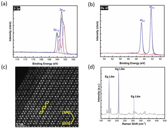
Figure 1.
(a) S 2p and (b) Re 4f X-ray photoelectron spectroscopy (XPS) core level spectra obtained on a freshly exfoliated ReS2 surface. The additional component in the lower binding energy is shown in red for both spectra. (c) High-angle annular dark field (HAADF) presents only Re atoms and (d) Raman spectrum of exfoliated ReS2.
A flake from an exfoliated ReS2 sample was imaged using STEM, as shown by the plan view in Figure 1c. ReS2 has triclinic symmetry in the crystal structure, wherein Re atoms in the layer form a zigzag Re–Re chain [17,20,45]. Figure 1c provides a view of the crystalline structure of the ReS2, and shows that the four Re atoms are arranged in a diamond-like shape and form atomic chains. The atomic structure confirms the distorted 1T phase, as suggested by previous investigations [20,36,45]. The TEM data show the presence of only one dominant distorted 1T phase in the ReS2 flakes. To further study the crystal structure of ReS2, Raman spectroscopy was performed on as-exfoliated bulk ReS2, showing conclusive evidence of having a distorted 1T structure. Because of the low symmetry of the distorted 1T phase, 18 Raman peaks were found in the range of 100–500 cm−1 in bulk ReS2, consistent with previous studies [46,47]. The primary Raman active modes at 150.2 cm−1 and 211.0 cm−1, associated with Eg-like and Ag-like modes, are presented in Figure 1d [48,49].
Thermal ALD of Al2O3 on ReS2
The evolution of the Re 4f and S 2p core levels throughout the thermal ALD of Al2O3 is shown in Figure 2a. The Re 4f and S 2p core level spectra were obtained from the ReS2 surface after in-situ annealing, after the first successive half-cycle of TMA and H2O, after the fifth half-cycle of TMA and H2O, and following 10, 40, and 80 full cycles of Al2O3. Only the XPS of the first and fifth half-cycle exposures are shown, as no significant changes occurred in the surface chemistry in between these measurements. Figure 2a indicates that the ReS2 sample is free of any additional chemical states in the Re 4f or S 2p core levels throughout the thermal ALD process, other than the state discussed above (Figure 1a,b), and rhenium oxide or sulfur oxide compounds (Re–O, Re–O–S, or S–O bonds) are below the XPS detection limit. The acquisition of XPS spectra for the Re 4f and S 2p core levels were extended on the higher binding energy side up to 55 eV and 175 eV (Figure 1a,b), respectively, to ensure that there were no additional chemical states at the Re 4f and S 2p core level spectra. Depositing Al2O3 on ReS2 decreases the intensities of the Re 4f and S 2p core levels (Figure 2a) due to XPS signal attenuation. However, the Re 4f and S 2p core levels are still clearly detectable even after 80 full cycles of thermal ALD due to the clustering of the Al2O3 film, as suggested by the ex-situ AFM topographic image in Figure 2b. At the initial stage, the slow growth rate indicates that thermal ALD of Al2O3 on the untreated ReS2 surface requires 10 thermal ALD cycles to nucleate, displaying the substrate-inhibited growth.
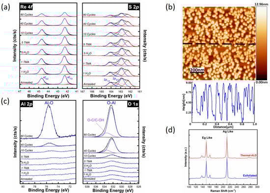
Figure 2.
Thermal atomic layer deposition (ALD) of Al2O3 on ReS2. (a) The evolution of Re 4f and S 2p core level spectra, (b) Ex-situ AFM image and line profile recorded following 80 cycles ALD of Al2O3, (c) Al 2p and O 1s core level spectra up to 80 cycles of Al2O3, and (d) Raman spectra comparison between exfoliated ReS2 and following 80 cycles of ALD of Al2O3.
Figure 2b shows a topographic image obtained by AFM of Al2O3 on ReS2 following 80 full cycles employing the thermal ALD process. After the thermal ALD on ReS2, an islanding growth is observed because of the relative dearth of dangling bonds on 2D TMD surfaces [25,26]. The AFM line profile shows that the height of these Al2O3 islands is ~8 nm, with a root mean square (RMS) surface roughness of 2.7 nm.
The corresponding Al 2p and O 1s core level spectra measured during the thermal ALD process are shown in Figure 2c. Aluminum remains near the XPS detection limit in the Al 2p core level following Al2O3 deposition up to 10 thermal ALD cycles. After 10 full cycles of Al2O3, the peak at 75.4 eV caused by the formation of Al–O bonds starts to increase, with an increasing number of ALD cycles. The analysis of this peak in the Al 2p core level after 40 and 80 full cycles reveals the formation of an Al2O3 film on ReS2. The line shape of the background intensity at the Al 2p core level increases at lower binding energies due to the presence of a Re 4f loss feature at 68 eV (Figure S3). After annealing, a small amount of oxygen (7.0 atomic%) was still detectable on the surface of the ReS2 sample (Figure 2c). The O 1s core level shown in Figure 2c after 40 and 80 full ALD cycles is deconvoluted into two peaks. The peak at 532.3 eV is associated with the Al−O chemical state and the peak at the higher binding energy (533.5 eV) is attributed to intermediate species, such as carbonyl and formate [28,50].
ReS2 samples characterized via ex-situ Raman spectroscopy following thermal ALD are consistent with the Raman spectra recorded on an as-exfoliated ReS2 surface [46,47]. Amorphous Al2O3 on the surface does not affect the Raman spectra of the substrate, and therefore structural changes through different processes of this work should be observable. Figure 2d shows the Raman spectra from as-exfoliated ReS2 and after 80 cycles thermal ALD of Al2O3. Two prominent Raman peaks at 150.2 cm−1 and 211.0 cm−1 are assigned to Eg-like and Ag-like vibrational modes, respectively [51]. In TMDs, Raman active modes have been reported to shift with changes in strain [52], temperature [53], and doping [54]. Figure 2d confirms that ReS2 remains unaffected following the annealing and the ALD process.
3.2. Plasma-Enhanced ALD of Al2O3 on ReS2
PEALD has been reported to achieve conformal high-κ dielectrics on the TMD surface without utilizing any surface pretreatment [55]. Based on this study, PEALD is used to improve the coverage of deposited Al2O3 on ReS2. More importantly, this work studies the interfacial chemistry changes during the PEALD process on ReS2. Similar to the thermal ALD process, an in-situ half-cycle PEALD study was performed to monitor the chemistry of the Al2O3/ReS2 interface. Figure 3a shows the Re 4f and S 2p core level spectra obtained from the annealed surface, after the first half-cycle of O2 plasma and TMA, after the fifth half-cycles of O2 plasma and TMA, and following 10, 40, and 80 full cycles of Al2O3. No additional chemical states were detected in the Re 4f or S 2p core levels on the surface of the annealed ReS2 sample. After the first pulse of remote O2 plasma, an additional chemical state in the corresponding S 2p core level was detected at 164.8 eV (Figure 3a, green peaks), which was concurrent with the appearance of an additional chemical state at a lower binding energy (530.5 eV) in the corresponding O 1s core level in Figure 3c.
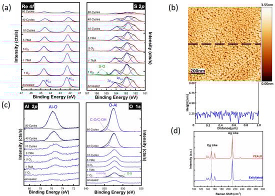
Figure 3.
Plasma-enhanced atomic layer deposition (PEALD) of Al2O3 on ReS2. (a) The evolution of (a) Re 4f and S 2p core level spectra, (b) Ex-situ AFM image and line profile recorded following 80 cycles PEALD of Al2O3, (c) Al 2p and O 1s core level spectra up to 80 cycles of Al2O3, and (d) Raman spectra recorded on exfoliated ReS2 and after 80 cycles of PEALD of Al2O3.
This additional chemical state corresponds to the S–O bonds created by the remote O2 plasma pulse. We estimated an oxidation of ~4.0% of S atoms on the surface after the first O2 plasma pulse. The S–O chemical bonds on the ReS2 surface act as nucleation sites, making the surface more reactive with the precursors. Through ligand exchange reactions, the S–O bonds are cleaned up by the successive TMA pulse and fall below the XPS detection limit [56]. During the rest of the PEALD process, the S–O chemical state remains below the XPS detection limit, and the ReS2 surface is free of any additional chemical states in the Re 4f or S 2p core levels, consistent with an abrupt interface. The first noticeable observation is that depositing Al2O3 on ReS2 using PEALD significantly decreases the intensities of the Re 4f and S 2p core levels from the substrate after 80 full cycles of PEALD, in comparison to thermal ALD (Figure 2a), which suggests better Al2O3 coverage on ReS2. This is consistent with the corresponding AFM topographic image in Figure 3b. The difference in thermal ALD and PEALD deposition after 80 cycles could be explained with the creation of S–O bonds as a reactive nucleation center in the PEALD method. Figure 3b shows the surface morphology of the sample after 80 PEALD cycles of Al2O3. The PEALD process results in a better coverage of the Al2O3 film with an RMS surface roughness of 0.49 nm compared to the thermal ALD process. The XPS-estimated Al2O3 thickness was 2.3 nm, which was calculated based on the substrate signal attenuation of the S 2p core level integrated intensity (Supplementary Materials, Section 3). The thickness calculated by XPS is underestimated due to the detection of the substrate signal through pinholes in the oxide film.
Figure 3c shows the evolution of the Al 2p and O 1s core level spectra of the PEALD process. Unlike the thermal ALD process, a small Al 2p peak is detected at 75.4 eV after the first TMA pulse, suggesting that, with the PEALD process, Al is deposited on the ReS2 surface without any inhibition time. The peak associated with the Al–O chemical state in Al 2p and O 1s core level spectra keeps increasing throughout the PEALD process. Similar to the thermal ALD process, the O 1s core level is deconvoluted into two main components of an Al–O chemical state at a low binding energy and an intermediate species chemical state at a higher binding energy. The ReS2 structure was monitored via ex-situ Raman spectroscopy before and after the PEALD (Figure 3d). The two prominent Raman peaks—Eg-like at 150.2 cm−1 and Ag-like at 211.0 cm−1—do not show any noticeable changes, confirming the stability of the ReS2 structure under the remote O2 plasma exposure of PEALD process.
The PEALD method results in a better coverage and lower root mean square (RMS) surface roughness due to a better nucleation and thus a thicker Al2O3 layer, as suggested by the associated XPS and AFM measurements. The PEALD of Al2O3 is greatly improved the low coverage and clustering behavior associated with the thermal ALD of Al2O3 on ReS2, however, pinholes with ~2 nm depth are observed, based on AFM measurements. Despite the improvement in Al2O3 coverage achieved with the PEALD process via the creation of S–O bonds, neither thermal ALD or PEALD yield conformal, pinhole-free Al2O3 on ReS2.
3.3. Al2O3 on A UV-Ozone Exposed ReS2 Surface
To grow a uniform dielectric layer on TMDs, a number of surface functionalization methods were proposed, such as UV-Ozone pre-treatment [26,57], oxygen plasma pre-treatment [58], the use of ozone as the oxidant precursor during the ALD of Al2O3 [28], and metal-oxide seed layers [59]. Based on the PEALD results of this work on ReS2 and the previous study on MoS2 [26,60], the formation of S–O in sulfur-based TMD materials seems to be a promising route for surface functionalization. To further improve the surface coverage of Al2O3 on the ReS2, the sample is exposed to UV-Ozone as a surface pretreatment to form S–O bonds, and then subjected to the standard thermal ALD process. An in-situ study of the UV-Ozone exposure of ReS2 was performed and chemical state changes were monitored by XPS. The UV photons from a low-pressure mercury lamp were used to produce ozone in a chamber (base pressure of ~10−9 mbar) which was filled with O2 to a pressure of 900 mbar [61]. Then, the sample was transferred in-situ to the ALD chamber for Al2O3 deposition with TMA and H2O. Figure 4a shows the Re 4f and S 2p core level spectra obtained from the annealed surface after 15 min UV-Ozone exposure, after the first successive half-cycle of H2O and TMA, after the fifth half-cycle of H2O and TMA, and following 10, 40, and 80 full cycles of Al2O3. After UV-Ozone exposure, an additional chemical state is detected in the S 2p core level at 164.8 eV (Figure 4a), which suggests the formation of S–O bonds [26]. The Re–O chemical state is below the XPS detection limit after the UV-Ozone exposure. We estimate ~12% of S atoms on the surface are oxidized after UV-Ozone treatment, but the S/Re ratio remains identical to the initial substrate. Following the first pulse of TMA, the S–O chemical state falls below the XPS detection limit. Similar to the PEALD process, during the rest of the thermal ALD process the S–O chemical state stays under the XPS detection limit. After 80 cycles of TMA/H2O deposition, sulfur is below the XPS detection limit due to the signal attenuation of the deposited Al2O3. In addition, the Re 4f core level intensity is significantly decreased, making it difficult to deconvolve. Significant attenuation of Re 4f and S 2p core levels suggest that Al2O3 is comparable to the XPS depth of detection (~5 nm). The topographical AFM image of the Al2O3 film following 80 full cycles of Al2O3 deposition through the thermal ALD on a UV-Ozone pretreated ReS2 surface is shown in Figure 4b. The AFM image shows a conformal and pinhole free film with a very low RMS roughness of 0.11 nm, consistent with XPS analysis.
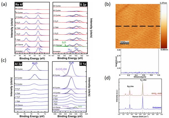
Figure 4.
Deposition of Al2O3 using thermal ALD on functionalized ReS2 surface by UV-Ozone exposure. (a) The evolution of Re 4f and S 2p core level spectra, (b) Ex-situ AFM image and line profile recorded following 80 cycles PEALD of Al2O3, (c) Al 2p and O 1s core level spectra up to 80 cycles of Al2O3, and (d) Raman spectra from exfoliated ReS2 and after 80 cycles of Al2O3 on UV-Ozone treated ReS2.
Figure 4c shows the evolution of the Al 2p and O 1s core level spectra. In the Al 2p core level, a peak is discernable at ~75 eV after the first TMA exposure, however, it is in the order of the XPS detection limit until the fifth TMA pulse. The O 1s core level again indicates the presence of two main components: an Al–O chemical state at low binding energy and an intermediate species chemical state at high binding energy. Utilizing the UV-Ozone pretreatment as a surface functionalization to deposit a thin Al2O3 film by thermal ALD produces the highest quality (conformal, pinhole-free) film on ReS2 in this work. The ex-situ Raman spectra of the ReS2 sample before and after being exposed to UV-Ozone at room temperature for 15 min and following 80 cycles of thermal ALD are shown in Figure 4d. Similar to the other processes, the Raman spectra did not show any changes after UV-Ozone exposure, demonstrating that the ReS2 structure stays intact.
Although both PEALD and the UV-Ozone pretreatment create S–O bonding on the surface, which serves as nucleation centers for subsequent ALD, the difference in the nucleation and Al2O3 growth behavior between the two methods is clear from AFM images. One important difference is that a higher S–O concentration was found for the UV-Ozone exposure in comparison to after the first O2 pulse in PEALD. This higher concentration of S–O bonds on the ReS2 surface helped with the pinhole issue of PEALD. Moreover, the concentration of the organic surface contamination after the UV-Ozone process is significantly less than after the PEALD process, as shown in the C 1s and O 1s XPS core level spectra (Figure S4). It is important to note that the prolonged X-ray exposure and UHV conditions occurred during the half-cycle XPS study do not change the surface chemistry of bulk ReS2 sample as indicated in Figure S5.
4. Conclusions
In summary, to achieve pinhole free and conformal high-κ dielectric on ReS2 substrate, we investigated different approaches for the growth of Al2O3. In-situ half-cycle XPS and ex-situ AFM were exploited to study the surface/interface chemistry and morphology of ReS2 after thermal ALD, PEALD, and UV-Ozone surface functionalization prior to ALD. Half-cycle XPS revealed that the ReS2 initial surface changes after the few first pulses of each process. The growth of Al2O3 by traditional ALD follows a substrate inhibited growth behavior, where an incubation period is required, followed by an islanding growth mode. However, the PEALD process enhances the growth of deposited Al2O3 by the creation of S–O bonds, but pinholes are still detectable even with lower RMS in comparison to the ALD growth. AFM images in conjunction with XPS data show that the UV-Ozone treatment is a practical route for the functionalization of ReS2 prior to ALD, to get a conformal coverage of Al2O3. Raman Spectroscopy and the XPS S/Re ratio confirms the structural stability of ReS2 under O2 plasma and UV-Ozone treatment.
Supplementary Materials
The following are available online at https://www.mdpi.com/1996-1944/12/7/1056/s1, Figure S1: C 1s, O 1s, Re 4f, and S 2p core level spectra of initial ReS2 and subsequent annealing, Figure S2: In-situ half-cycle ALD/PEALD process, Figure S3: Wider XPS region of Al 2p, Section 4: XPS-calculated thickness, Figure S4: O 1s and C 1s core level spectra comparison, Figure S5: Re 4f and S 2p core level spectra of the exfoliated ReS2 sample after long x-ray exposure and being in UHV environment.
Author Contributions
Conceptualization, A.K., R.A., and R.W.; methodology, A.K., M.C.; formal analysis, A.K.; writing—original draft preparation, A.K.; writing—review and editing, R.A., M.C., J.K., and R.W.
Funding
This work was supported in part by NEWLIMITS, a center in nCORE, a Semiconductor Research Corporation (SRC) program sponsored by NIST through award number 70NANB17H041.
Acknowledgments
The authors acknowledge Christopher Smyth and Antonio T. Lucero for useful discussions.
Conflicts of Interest
The authors declare no conflict of interest.
References
- Amani, M.; Chin, M.L.; Birdwell, A.G.; O’Regan, T.P.; Najmaei, S.; Liu, Z.; Ajayan, P.M.; Lou, J.; Dubey, M. Electrical performance of monolayer MoS2 field-effect transistors prepared by chemical vapor deposition. Appl. Phys. Lett. 2013, 102, 193107. [Google Scholar] [CrossRef]
- Nourbakhsh, A.; Zubair, A.; Sajjad, R.N.; Tavakkoli KG, A.; Chen, W.; Fang, S.; Ling, X.; Kong, J.; Dresselhaus, M.S.; Kaxiras, E. MoS2 field-effect transistor with sub-10 nm channel length. Nano Lett. 2016, 16, 7798–7806. [Google Scholar] [CrossRef] [PubMed]
- Akinwande, D.; Petrone, N.; Hone, J. Two-dimensional flexible nanoelectronics. Nat. Commun. 2014, 5, 5678. [Google Scholar] [CrossRef]
- Wang, Q.H.; Kalantar-Zadeh, K.; Kis, A.; Coleman, J.N.; Strano, M.S. Electronics and optoelectronics of two-dimensional transition metal dichalcogenides. Nat. Nanotechnol. 2012, 7, 699. [Google Scholar] [CrossRef] [PubMed]
- Tongay, S.; Sahin, H.; Ko, C.; Luce, A.; Fan, W.; Liu, K.; Zhou, J.; Huang, Y.-S.; Ho, C.-H.; Yan, J. Monolayer behaviour in bulk ReS2 due to electronic and vibrational decoupling. Nat. Commun. 2014, 5, 3252. [Google Scholar] [CrossRef] [PubMed]
- Horzum, S.; Çakır, D.; Suh, J.; Tongay, S.; Huang, Y.-S.; Ho, C.-H.; Wu, J.; Sahin, H.; Peeters, F. Formation and stability of point defects in monolayer rhenium disulfide. Phys. Rev. B 2014, 89, 155433. [Google Scholar] [CrossRef]
- Yu, Z.G.; Cai, Y.; Zhang, Y.-W. Robust Direct Bandgap Characteristics of One-and Two-Dimensional ReS2. Sci. Rep. 2015, 5, 13783. [Google Scholar] [CrossRef] [PubMed]
- Zong, J.-Q.; Zhang, S.-F.; Ji, W.-X.; Zhang, C.-W.; Li, P.; Wang, P.-J. Electric structure and optical properties of ReS2 nanomaterials. Superlattice Microst. 2018, 122, 262–267. [Google Scholar] [CrossRef]
- Echeverry, J.; Gerber, I. Theoretical investigations of the anisotropic optical properties of distorted 1T ReS2 and ReSe2 monolayers, bilayers, and in the bulk limit. Phys. Rev. B 2018, 97, 075123. [Google Scholar] [CrossRef]
- Gutiérrez-Lezama, I.; Reddy, B.A.; Ubrig, N.; Morpurgo, A.F. Electroluminescence from indirect band gap semiconductor ReS2. 2D Mater. 2016, 3, 045016. [Google Scholar] [CrossRef]
- Webb, J.L.; Hart, L.S.; Wolverson, D.; Chen, C.; Avila, J.; Asensio, M.C. Electronic band structure of ReS2 by high-resolution angle-resolved photoemission spectroscopy. Phys. Rev. B 2017, 96, 115205. [Google Scholar] [CrossRef]
- Gehlmann, M.; Aguilera, I.; Bihlmayer, G.; Nemsák, S.; Nagler, P.; Gospodaric, P.; Zamborlini, G.; Eschbach, M.; Feyer, V.; Kronast, F. Direct observation of the band gap transition in atomically thin ReS2. Nano Lett. 2017, 17, 5187–5192. [Google Scholar] [CrossRef] [PubMed]
- Gunasekera, S.M.; Wolverson, D.; Hart, L.S.; Mucha-Kruczynski, M. Electronic band structure of rhenium dichalcogenides. J. Electron. Mater. 2018, 47, 1–7. [Google Scholar] [CrossRef]
- Hart, L.S.; Webb, J.L.; Dale, S.; Bending, S.J.; Mucha-Kruczynski, M.; Wolverson, D.; Chen, C.; Avila, J.; Asensio, M.C. Electronic bandstructure and van der Waals coupling of ReSe2 revealed by high-resolution angle-resolved photoemission spectroscopy. Sci. Rep. 2017, 7, 5145. [Google Scholar] [CrossRef] [PubMed]
- Corbet, C.M.; McClellan, C.; Rai, A.; Sonde, S.S.; Tutuc, E.; Banerjee, S.K. Field effect transistors with current saturation and voltage gain in ultrathin ReS2. ACS Nano 2014, 9, 363–370. [Google Scholar] [CrossRef] [PubMed]
- Zhang, E.; Jin, Y.; Yuan, X.; Wang, W.; Zhang, C.; Tang, L.; Liu, S.; Zhou, P.; Hu, W.; Xiu, F. ReS2-Based Field-Effect Transistors and Photodetectors. Adv. Funct. Mater. 2015, 25, 4076–4082. [Google Scholar] [CrossRef]
- He, X.; Liu, F.; Hu, P.; Fu, W.; Wang, X.; Zeng, Q.; Zhao, W.; Liu, Z. Chemical Vapor Deposition of High-Quality and Atomically Layered ReS2. Small 2015, 11, 5423–5429. [Google Scholar] [CrossRef] [PubMed]
- Shim, J.; Oh, A.; Kang, D.H.; Oh, S.; Jang, S.K.; Jeon, J.; Jeon, M.H.; Kim, M.; Choi, C.; Lee, J. High-Performance 2D Rhenium Disulfide (ReS2) Transistors and Photodetectors by Oxygen Plasma Treatment. Adv. Mater. 2016, 28, 6985–6992. [Google Scholar] [CrossRef] [PubMed]
- Liu, E.; Fu, Y.; Wang, Y.; Feng, Y.; Liu, H.; Wan, X.; Zhou, W.; Wang, B.; Shao, L.; Ho, C.-H. Integrated digital inverters based on two-dimensional anisotropic ReS2 field-effect transistors. Nat. Commun. 2015, 6, 6991. [Google Scholar] [CrossRef] [PubMed]
- Lin, Y.-C.; Komsa, H.-P.; Yeh, C.-H.; Bjorkman, T.; Liang, Z.-Y.; Ho, C.-H.; Huang, Y.-S.; Chiu, P.-W.; Krasheninnikov, A.V.; Suenaga, K. Single-layer ReS2: Two-dimensional semiconductor with tunable in-plane anisotropy. ACS Nano 2015, 9, 11249–11257. [Google Scholar] [CrossRef]
- Liao, W.; Wei, W.; Tong, Y.; Chim, W.K.; Zhu, C. Low-Frequency Noise in Layered ReS2 Field Effect Transistors on HfO2 and Its Application for pH Sensing. ACS Appl. Mater. Interfaces 2018, 10, 7248–7255. [Google Scholar] [CrossRef]
- Park, J.Y.; Joe, H.-E.; Yoon, H.S.; Yoo, S.; Kim, T.; Kang, K.; Min, B.-K.; Jun, S.C. Contact effect of ReS2/metal interface. ACS Appl. Mater. Interfaces 2017, 9, 26325–26332. [Google Scholar] [CrossRef] [PubMed]
- Addou, R.; Wallace, R.M. Using Photoelectron Spectroscopy in the Integration of 2D Materials for Advanced Devices. J. Electron. Spectrosc. Relat. Phenom. 2019, 231, 94–103. [Google Scholar] [CrossRef]
- Jena, D.; Konar, A. Enhancement of carrier mobility in semiconductor nanostructures by dielectric engineering. Phys. Rev. Lett. 2007, 98, 136805. [Google Scholar] [CrossRef] [PubMed]
- McDonnell, S.; Brennan, B.; Azcatl, A.; Lu, N.; Dong, H.; Buie, C.; Kim, J.; Hinkle, C.L.; Kim, M.J.; Wallace, R.M. HfO2 on MoS2 by atomic layer deposition: Adsorption mechanisms and thickness scalability. ACS Nano 2013, 7, 10354–10361. [Google Scholar] [CrossRef]
- Azcatl, A.; McDonnell, S.; KC, S.; Peng, X.; Dong, H.; Qin, X.; Addou, R.; Mordi, G.I.; Lu, N.; Kim, J. MoS2 functionalization for ultra-thin atomic layer deposited dielectrics. Appl. Phys. Lett. 2014, 104, 111601. [Google Scholar] [CrossRef]
- Azcatl, A.; Wang, Q.; Kim, M.J.; Wallace, R.M. Al2O3 on WSe2 by ozone based atomic layer deposition: Nucleation and interface study. APL Mater. 2017, 5, 086108. [Google Scholar] [CrossRef]
- Cheng, L.; Qin, X.; Lucero, A.T.; Azcatl, A.; Huang, J.; Wallace, R.M.; Cho, K.; Kim, J. Atomic layer deposition of a high-k dielectric on MoS2 using trimethylaluminum and ozone. ACS Appl. Mater. Interfaces 2014, 6, 11834–11838. [Google Scholar] [CrossRef]
- Zhu, H.; McDonnell, S.; Qin, X.; Azcatl, A.; Cheng, L.; Addou, R.; Kim, J.; Ye, P.D.; Wallace, R.M. Al2O3 on black phosphorus by atomic layer deposition: An in-situ interface study. ACS Appl. Mater. Interfaces 2015, 7, 13038–13043. [Google Scholar] [CrossRef]
- Dahal, A.; Addou, R.; Azcatl, A.; Coy-Diaz, H.; Lu, N.; Peng, X.; de Dios, F.; Kim, J.; Kim, M.J.; Wallace, R.M. Seeding Atomic Layer Deposition of Alumina on Graphene with Yttria. ACS Appl. Mater. Interfaces 2015, 7, 2082–2087. [Google Scholar] [CrossRef]
- Addou, R.; Dahal, A.; Batzill, M. Growth of a two-dimensional dielectric monolayer on quasi-freestanding graphene. Nat. Nanotechnol. 2013, 8, 41. [Google Scholar] [CrossRef] [PubMed]
- Wallace, R.M. In-Situ Studies on 2D Materials. ECS Trans. 2014, 64, 109–116. [Google Scholar] [CrossRef]
- Herrera-Gomez, A.; Hegedus, A.; Meissner, P. Chemical depth profile of ultrathin nitrided SiO2 films. Appl. Phys. Lett. 2002, 81, 1014–1016. [Google Scholar] [CrossRef]
- Horcas, I.; Fernández, R.; Gomez-Rodriguez, J.; Colchero, J.; Gómez-Herrero, J.; Baro, A. WSXM: A software for scanning probe microscopy and a tool for nanotechnology. Rev. Sci. Instrum. 2007, 78, 013705. [Google Scholar] [CrossRef] [PubMed]
- Xie, L.; Wang, J.; Shi, C.; Huang, J.; Zhang, H.; Liu, Q.; Liu, Q.; Zeng, H. Probing surface interactions of electrochemically active galena mineral surface using atomic force microscopy. J. Phys. Chem. C 2016, 120, 22433–22442. [Google Scholar] [CrossRef]
- Cui, F.; Wang, C.; Li, X.; Wang, G.; Liu, K.; Yang, Z.; Feng, Q.; Liang, X.; Zhang, Z.; Liu, S. Tellurium-Assisted Epitaxial Growth of Large-Area, Highly Crystalline ReS2 Atomic Layers on Mica Substrate. Adv. Mater. 2016, 28, 5019–5024. [Google Scholar] [CrossRef] [PubMed]
- Wang, L.; Sofer, Z.; Luxa, J.; Sedmidubský, D.; Ambrosi, A.; Pumera, M. Layered rhenium sulfide on free-standing three-dimensional electrodes is highly catalytic for the hydrogen evolution reaction: Experimental and theoretical study. Electrochem. Commun. 2016, 63, 39–43. [Google Scholar] [CrossRef]
- Zhang, Q.; Tan, S.; Mendes, R.G.; Sun, Z.; Chen, Y.; Kong, X.; Xue, Y.; Rümmeli, M.H.; Wu, X.; Chen, S. Extremely Weak van der Waals Coupling in Vertical ReS2 Nanowalls for High-Current-Density Lithium-Ion Batteries. Adv. Mater. 2016, 28, 2616–2623. [Google Scholar] [CrossRef]
- Fujita, T.; Ito, Y.; Tan, Y.; Yamaguchi, H.; Hojo, D.; Hirata, A.; Voiry, D.; Chhowalla, M.; Chen, M. Chemically exfoliated ReS2 nanosheets. Nanoscale 2014, 6, 12458–12462. [Google Scholar] [CrossRef] [PubMed]
- Jariwala, B.; Voiry, D.; Jindal, A.; Chalke, B.A.; Bapat, R.; Thamizhavel, A.; Chhowalla, M.; Deshmukh, M.; Bhattacharya, A. Synthesis and characterization of ReS2 and ReSe2 layered chalcogenide single crystals. Chem. Mater. 2016, 28, 3352–3359. [Google Scholar] [CrossRef]
- Hafeez, M.; Gan, L.; Li, H.; Ma, Y.; Zhai, T. Large-Area Bilayer ReS2 Film/Multilayer ReS2 Flakes Synthesized by Chemical Vapor Deposition for High Performance Photodetectors. Adv. Funct. Mater. 2016, 26, 4551–4560. [Google Scholar] [CrossRef]
- Wei, J.; Bai, D.; Yang, L. Polymer photovoltaic cells with rhenium oxide as anode interlayer. PLoS ONE 2015, 10, e0133725. [Google Scholar] [CrossRef] [PubMed]
- Addou, R.; McDonnell, S.; Barrera, D.; Guo, Z.; Azcatl, A.; Wang, J.; Zhu, H.; Hinkle, C.L.; Quevedo-Lopez, M.; Alshareef, H.N. Impurities and electronic property variations of natural MoS2 crystal surfaces. ACS Nano 2015, 9, 9124–9133. [Google Scholar] [CrossRef]
- Keyshar, K.; Gong, Y.; Ye, G.; Brunetto, G.; Zhou, W.; Cole, D.P.; Hackenberg, K.; He, Y.; Machado, L.; Kabbani, M. Chemical vapor deposition of monolayer rhenium disulfide (ReS2). Adv. Mater. 2015, 27, 4640–4648. [Google Scholar] [CrossRef]
- Rahman, M.; Davey, K.; Qiao, S.Z. Advent of 2D rhenium disulfide (ReS2): Fundamentals to applications. Adv. Funct. Mater. 2017, 27, 1606129. [Google Scholar] [CrossRef]
- Feng, Y.; Zhou, W.; Wang, Y.; Zhou, J.; Liu, E.; Fu, Y.; Ni, Z.; Wu, X.; Yuan, H.; Miao, F. Raman vibrational spectra of bulk to monolayer ReS2 with lower symmetry. Phys. Rev. B 2015, 92, 054110. [Google Scholar] [CrossRef]
- Miao, P.; Qin, J.K.; Shen, Y.; Su, H.; Dai, J.; Song, B.; Du, Y.; Sun, M.; Zhang, W.; Wang, H.L. Unraveling the Raman Enhancement Mechanism on 1T′-Phase ReS2 Nanosheets. Small 2018, 14, 1704079. [Google Scholar] [CrossRef]
- Lee, B.C.; Na, J.; Choi, J.H.; Ji, H.; Kim, G.T.; Joo, M.K. Probing Distinctive Electron Conduction in Multilayer Rhenium Disulfide. Adv. Mater. 2018, 31, 1805860. [Google Scholar] [CrossRef] [PubMed]
- Wang, X.; Shinokita, K.; Lim, H.E.; Mohamed, N.B.; Miyauchi, Y.; Cuong, N.T.; Okada, S.; Matsuda, K. Direct and Indirect Exciton Dynamics in Few-Layered ReS2 Revealed by Photoluminescence and Pump-Probe Spectroscopy. Adv. Funct. Mater. 2018, 29, 1806169. [Google Scholar] [CrossRef]
- Pirkle, A.; McDonnell, S.; Lee, B.; Kim, J.; Colombo, L.; Wallace, R. The effect of graphite surface condition on the composition of Al2O3 by atomic layer deposition. Appl. Phys. Lett. 2010, 97, 082901. [Google Scholar] [CrossRef]
- Liu, D.; Hong, J.; Wang, X.; Li, X.; Feng, Q.; Tan, C.; Zhai, T.; Ding, F.; Peng, H.; Xu, H. Diverse Atomically Sharp Interfaces and Linear Dichroism of 1T’ ReS2-ReSe2 Lateral p-n Heterojunctions. Adv. Funct. Mater. 2018, 1804696. [Google Scholar] [CrossRef]
- Azcatl, A.; Qin, X.; Prakash, A.; Zhang, C.; Cheng, L.; Wang, Q.; Lu, N.; Kim, M.J.; Kim, J.; Cho, K. Covalent nitrogen doping and compressive strain in MoS2 by remote N2 plasma exposure. Nano Lett. 2016, 16, 5437–5443. [Google Scholar] [CrossRef] [PubMed]
- Cho, S.; Kim, S.; Kim, J.H.; Zhao, J.; Seok, J.; Keum, D.H.; Baik, J.; Choe, D.-H.; Chang, K.J.; Suenaga, K. Phase patterning for ohmic homojunction contact in MoTe2. Science 2015, 349, 625–628. [Google Scholar] [CrossRef]
- Khosravi, A.; Addou, R.; Smyth, C.M.; Yue, R.; Cormier, C.R.; Kim, J.; Hinkle, C.L.; Wallace, R.M. Covalent nitrogen doping in molecular beam epitaxy-grown and bulk WSe2. APL Mater. 2018, 6, 026603. [Google Scholar] [CrossRef]
- Price, K.M.; Schauble, K.E.; McGuire, F.A.; Farmer, D.B.; Franklin, A.D. Uniform Growth of Sub-5-Nanometer High-κ Dielectrics on MoS2 Using Plasma-Enhanced Atomic Layer Deposition. ACS Appl. Mater. Interfaces 2017, 9, 23072–23080. [Google Scholar] [CrossRef]
- Hinkle, C.; Sonnet, A.; Vogel, E.; McDonnell, S.; Hughes, G.; Milojevic, M.; Lee, B.; Aguirre-Tostado, F.; Choi, K.; Kim, H. GaAs interfacial self-cleaning by atomic layer deposition. Appl. Phys. Lett. 2008, 92, 071901. [Google Scholar] [CrossRef]
- Zhao, P.; Khosravi, A.; Azcatl, A.; Bolshakov, P.; Mirabelli, G.; Caruso, E.; Hinkle, C.L.; Hurley, P.K.; Wallace, R.M.; Young, C.D. Evaluation of border traps and interface traps in HfO2/MoS2 gate stacks by capacitance-voltage analysis. 2D Mater. 2018, 5, 031002. [Google Scholar] [CrossRef]
- Yang, J.; Kim, S.; Choi, W.; Park, S.H.; Jung, Y.; Cho, M.-H.; Kim, H. Improved growth behavior of atomic-layer-deposited high-k dielectrics on multilayer MoS2 by oxygen plasma pretreatment. ACS Appl. Mater. Interfaces 2013, 5, 4739–4744. [Google Scholar] [CrossRef]
- Zou, X.; Wang, J.; Chiu, C.H.; Wu, Y.; Xiao, X.; Jiang, C.; Wu, W.W.; Mai, L.; Chen, T.; Li, J. Interface Engineering for High-Performance Top-Gated MoS2 Field-Effect Transistors. Adv. Mater. 2014, 26, 6255–6261. [Google Scholar] [CrossRef]
- McDonnell, S.J.; Wallace, R.M. UV-Ozone Functionalization of 2D Materials. JOM 2018, 1–14. [Google Scholar] [CrossRef]
- Wallace, R.M. In-Situ Studies of Interfacial Bonding of High-κ Dielectrics for CMOS Beyond 22 nm. Electrochem. Soc. Trans. 2008, 16, 255. [Google Scholar]
© 2019 by the authors. Licensee MDPI, Basel, Switzerland. This article is an open access article distributed under the terms and conditions of the Creative Commons Attribution (CC BY) license (http://creativecommons.org/licenses/by/4.0/).