High-κ Dielectric on ReS2: In-Situ Thermal Versus Plasma-Enhanced Atomic Layer Deposition of Al2O3


Abstract
1. Introduction
2. Materials and Methods
3. Results and Discussion
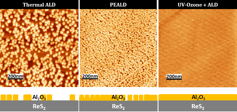
3.1. Surface Analysis of the Exfoliated ReS2 Surface
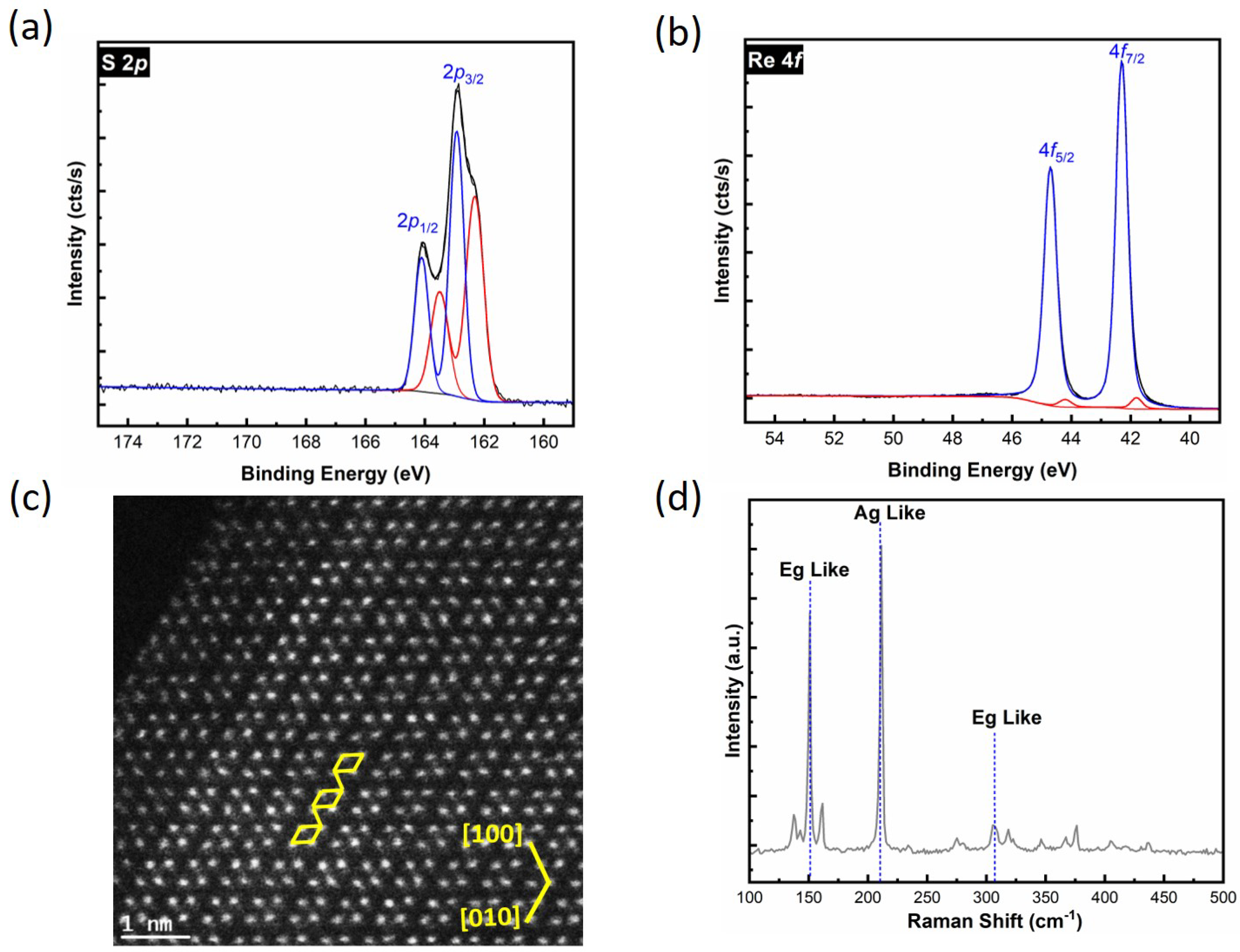
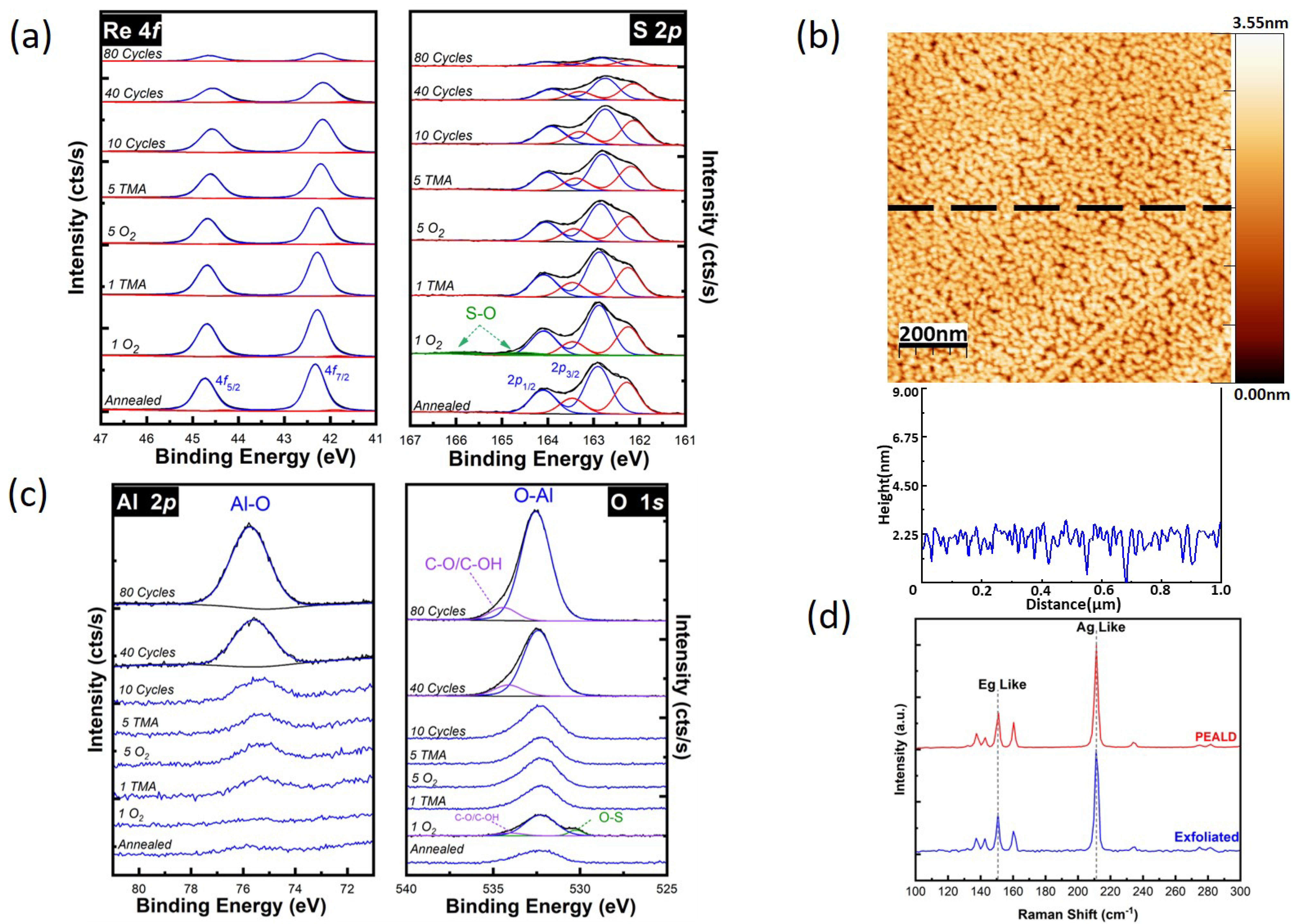
Thermal ALD of Al2O3 on ReS2
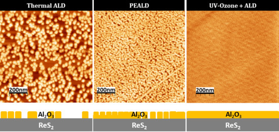
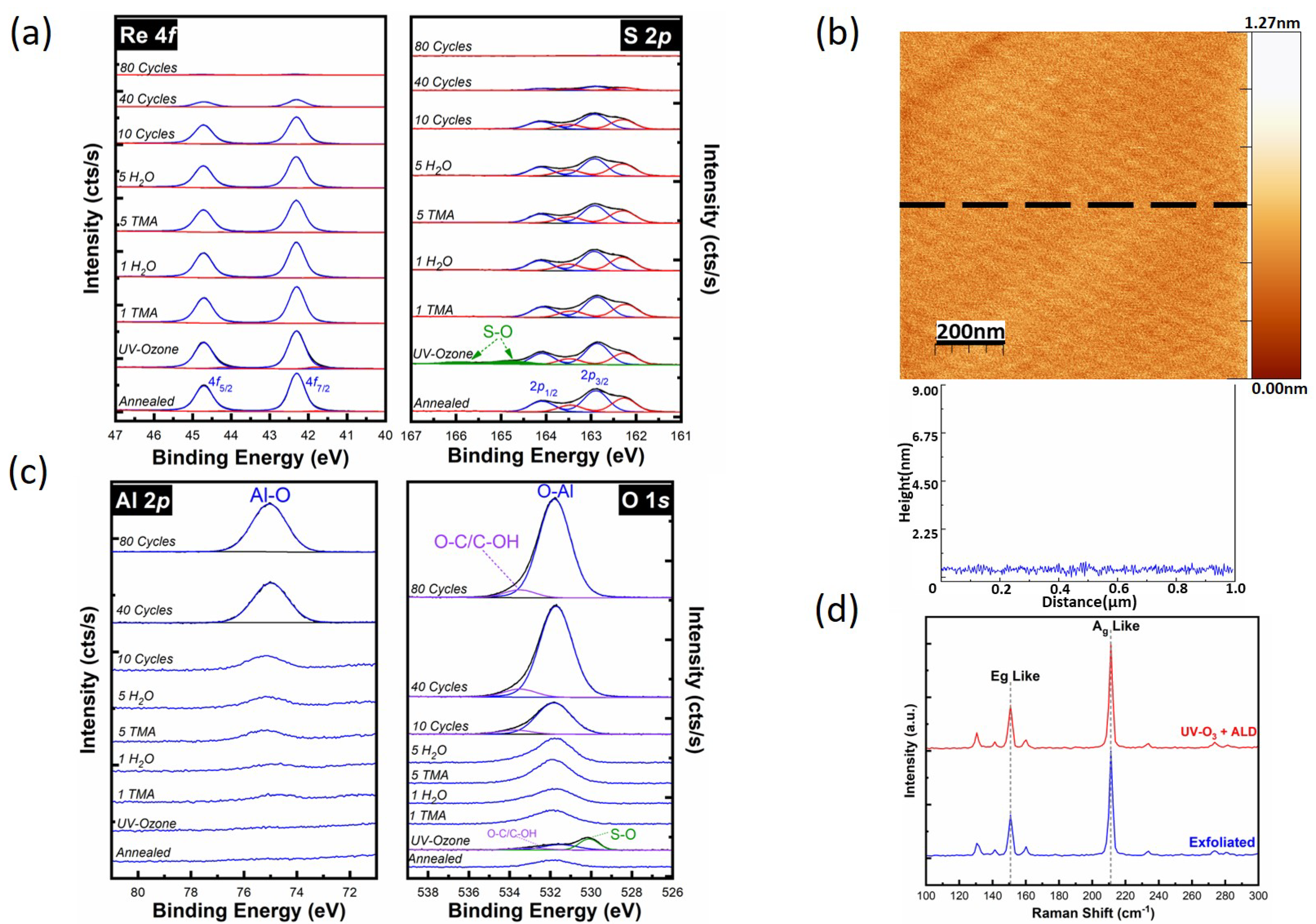
3.2. Plasma-Enhanced ALD of Al2O3 on ReS2
3.3. Al2O3 on A UV-Ozone Exposed ReS2 Surface
4. Conclusions
Supplementary Materials
Author Contributions
Funding
Acknowledgments
Conflicts of Interest
References
- Amani, M.; Chin, M.L.; Birdwell, A.G.; O’Regan, T.P.; Najmaei, S.; Liu, Z.; Ajayan, P.M.; Lou, J.; Dubey, M. Electrical performance of monolayer MoS2 field-effect transistors prepared by chemical vapor deposition. Appl. Phys. Lett. 2013, 102, 193107. [Google Scholar] [CrossRef]
- Nourbakhsh, A.; Zubair, A.; Sajjad, R.N.; Tavakkoli KG, A.; Chen, W.; Fang, S.; Ling, X.; Kong, J.; Dresselhaus, M.S.; Kaxiras, E. MoS2 field-effect transistor with sub-10 nm channel length. Nano Lett. 2016, 16, 7798–7806. [Google Scholar] [CrossRef] [PubMed]
- Akinwande, D.; Petrone, N.; Hone, J. Two-dimensional flexible nanoelectronics. Nat. Commun. 2014, 5, 5678. [Google Scholar] [CrossRef]
- Wang, Q.H.; Kalantar-Zadeh, K.; Kis, A.; Coleman, J.N.; Strano, M.S. Electronics and optoelectronics of two-dimensional transition metal dichalcogenides. Nat. Nanotechnol. 2012, 7, 699. [Google Scholar] [CrossRef] [PubMed]
- Tongay, S.; Sahin, H.; Ko, C.; Luce, A.; Fan, W.; Liu, K.; Zhou, J.; Huang, Y.-S.; Ho, C.-H.; Yan, J. Monolayer behaviour in bulk ReS2 due to electronic and vibrational decoupling. Nat. Commun. 2014, 5, 3252. [Google Scholar] [CrossRef] [PubMed]
- Horzum, S.; Çakır, D.; Suh, J.; Tongay, S.; Huang, Y.-S.; Ho, C.-H.; Wu, J.; Sahin, H.; Peeters, F. Formation and stability of point defects in monolayer rhenium disulfide. Phys. Rev. B 2014, 89, 155433. [Google Scholar] [CrossRef]
- Yu, Z.G.; Cai, Y.; Zhang, Y.-W. Robust Direct Bandgap Characteristics of One-and Two-Dimensional ReS2. Sci. Rep. 2015, 5, 13783. [Google Scholar] [CrossRef] [PubMed]
- Zong, J.-Q.; Zhang, S.-F.; Ji, W.-X.; Zhang, C.-W.; Li, P.; Wang, P.-J. Electric structure and optical properties of ReS2 nanomaterials. Superlattice Microst. 2018, 122, 262–267. [Google Scholar] [CrossRef]
- Echeverry, J.; Gerber, I. Theoretical investigations of the anisotropic optical properties of distorted 1T ReS2 and ReSe2 monolayers, bilayers, and in the bulk limit. Phys. Rev. B 2018, 97, 075123. [Google Scholar] [CrossRef]
- Gutiérrez-Lezama, I.; Reddy, B.A.; Ubrig, N.; Morpurgo, A.F. Electroluminescence from indirect band gap semiconductor ReS2. 2D Mater. 2016, 3, 045016. [Google Scholar] [CrossRef]
- Webb, J.L.; Hart, L.S.; Wolverson, D.; Chen, C.; Avila, J.; Asensio, M.C. Electronic band structure of ReS2 by high-resolution angle-resolved photoemission spectroscopy. Phys. Rev. B 2017, 96, 115205. [Google Scholar] [CrossRef]
- Gehlmann, M.; Aguilera, I.; Bihlmayer, G.; Nemsák, S.; Nagler, P.; Gospodaric, P.; Zamborlini, G.; Eschbach, M.; Feyer, V.; Kronast, F. Direct observation of the band gap transition in atomically thin ReS2. Nano Lett. 2017, 17, 5187–5192. [Google Scholar] [CrossRef] [PubMed]
- Gunasekera, S.M.; Wolverson, D.; Hart, L.S.; Mucha-Kruczynski, M. Electronic band structure of rhenium dichalcogenides. J. Electron. Mater. 2018, 47, 1–7. [Google Scholar] [CrossRef]
- Hart, L.S.; Webb, J.L.; Dale, S.; Bending, S.J.; Mucha-Kruczynski, M.; Wolverson, D.; Chen, C.; Avila, J.; Asensio, M.C. Electronic bandstructure and van der Waals coupling of ReSe2 revealed by high-resolution angle-resolved photoemission spectroscopy. Sci. Rep. 2017, 7, 5145. [Google Scholar] [CrossRef] [PubMed]
- Corbet, C.M.; McClellan, C.; Rai, A.; Sonde, S.S.; Tutuc, E.; Banerjee, S.K. Field effect transistors with current saturation and voltage gain in ultrathin ReS2. ACS Nano 2014, 9, 363–370. [Google Scholar] [CrossRef] [PubMed]
- Zhang, E.; Jin, Y.; Yuan, X.; Wang, W.; Zhang, C.; Tang, L.; Liu, S.; Zhou, P.; Hu, W.; Xiu, F. ReS2-Based Field-Effect Transistors and Photodetectors. Adv. Funct. Mater. 2015, 25, 4076–4082. [Google Scholar] [CrossRef]
- He, X.; Liu, F.; Hu, P.; Fu, W.; Wang, X.; Zeng, Q.; Zhao, W.; Liu, Z. Chemical Vapor Deposition of High-Quality and Atomically Layered ReS2. Small 2015, 11, 5423–5429. [Google Scholar] [CrossRef] [PubMed]
- Shim, J.; Oh, A.; Kang, D.H.; Oh, S.; Jang, S.K.; Jeon, J.; Jeon, M.H.; Kim, M.; Choi, C.; Lee, J. High-Performance 2D Rhenium Disulfide (ReS2) Transistors and Photodetectors by Oxygen Plasma Treatment. Adv. Mater. 2016, 28, 6985–6992. [Google Scholar] [CrossRef] [PubMed]
- Liu, E.; Fu, Y.; Wang, Y.; Feng, Y.; Liu, H.; Wan, X.; Zhou, W.; Wang, B.; Shao, L.; Ho, C.-H. Integrated digital inverters based on two-dimensional anisotropic ReS2 field-effect transistors. Nat. Commun. 2015, 6, 6991. [Google Scholar] [CrossRef] [PubMed]
- Lin, Y.-C.; Komsa, H.-P.; Yeh, C.-H.; Bjorkman, T.; Liang, Z.-Y.; Ho, C.-H.; Huang, Y.-S.; Chiu, P.-W.; Krasheninnikov, A.V.; Suenaga, K. Single-layer ReS2: Two-dimensional semiconductor with tunable in-plane anisotropy. ACS Nano 2015, 9, 11249–11257. [Google Scholar] [CrossRef]
- Liao, W.; Wei, W.; Tong, Y.; Chim, W.K.; Zhu, C. Low-Frequency Noise in Layered ReS2 Field Effect Transistors on HfO2 and Its Application for pH Sensing. ACS Appl. Mater. Interfaces 2018, 10, 7248–7255. [Google Scholar] [CrossRef]
- Park, J.Y.; Joe, H.-E.; Yoon, H.S.; Yoo, S.; Kim, T.; Kang, K.; Min, B.-K.; Jun, S.C. Contact effect of ReS2/metal interface. ACS Appl. Mater. Interfaces 2017, 9, 26325–26332. [Google Scholar] [CrossRef] [PubMed]
- Addou, R.; Wallace, R.M. Using Photoelectron Spectroscopy in the Integration of 2D Materials for Advanced Devices. J. Electron. Spectrosc. Relat. Phenom. 2019, 231, 94–103. [Google Scholar] [CrossRef]
- Jena, D.; Konar, A. Enhancement of carrier mobility in semiconductor nanostructures by dielectric engineering. Phys. Rev. Lett. 2007, 98, 136805. [Google Scholar] [CrossRef] [PubMed]
- McDonnell, S.; Brennan, B.; Azcatl, A.; Lu, N.; Dong, H.; Buie, C.; Kim, J.; Hinkle, C.L.; Kim, M.J.; Wallace, R.M. HfO2 on MoS2 by atomic layer deposition: Adsorption mechanisms and thickness scalability. ACS Nano 2013, 7, 10354–10361. [Google Scholar] [CrossRef]
- Azcatl, A.; McDonnell, S.; KC, S.; Peng, X.; Dong, H.; Qin, X.; Addou, R.; Mordi, G.I.; Lu, N.; Kim, J. MoS2 functionalization for ultra-thin atomic layer deposited dielectrics. Appl. Phys. Lett. 2014, 104, 111601. [Google Scholar] [CrossRef]
- Azcatl, A.; Wang, Q.; Kim, M.J.; Wallace, R.M. Al2O3 on WSe2 by ozone based atomic layer deposition: Nucleation and interface study. APL Mater. 2017, 5, 086108. [Google Scholar] [CrossRef]
- Cheng, L.; Qin, X.; Lucero, A.T.; Azcatl, A.; Huang, J.; Wallace, R.M.; Cho, K.; Kim, J. Atomic layer deposition of a high-k dielectric on MoS2 using trimethylaluminum and ozone. ACS Appl. Mater. Interfaces 2014, 6, 11834–11838. [Google Scholar] [CrossRef]
- Zhu, H.; McDonnell, S.; Qin, X.; Azcatl, A.; Cheng, L.; Addou, R.; Kim, J.; Ye, P.D.; Wallace, R.M. Al2O3 on black phosphorus by atomic layer deposition: An in-situ interface study. ACS Appl. Mater. Interfaces 2015, 7, 13038–13043. [Google Scholar] [CrossRef]
- Dahal, A.; Addou, R.; Azcatl, A.; Coy-Diaz, H.; Lu, N.; Peng, X.; de Dios, F.; Kim, J.; Kim, M.J.; Wallace, R.M. Seeding Atomic Layer Deposition of Alumina on Graphene with Yttria. ACS Appl. Mater. Interfaces 2015, 7, 2082–2087. [Google Scholar] [CrossRef]
- Addou, R.; Dahal, A.; Batzill, M. Growth of a two-dimensional dielectric monolayer on quasi-freestanding graphene. Nat. Nanotechnol. 2013, 8, 41. [Google Scholar] [CrossRef] [PubMed]
- Wallace, R.M. In-Situ Studies on 2D Materials. ECS Trans. 2014, 64, 109–116. [Google Scholar] [CrossRef]
- Herrera-Gomez, A.; Hegedus, A.; Meissner, P. Chemical depth profile of ultrathin nitrided SiO2 films. Appl. Phys. Lett. 2002, 81, 1014–1016. [Google Scholar] [CrossRef]
- Horcas, I.; Fernández, R.; Gomez-Rodriguez, J.; Colchero, J.; Gómez-Herrero, J.; Baro, A. WSXM: A software for scanning probe microscopy and a tool for nanotechnology. Rev. Sci. Instrum. 2007, 78, 013705. [Google Scholar] [CrossRef] [PubMed]
- Xie, L.; Wang, J.; Shi, C.; Huang, J.; Zhang, H.; Liu, Q.; Liu, Q.; Zeng, H. Probing surface interactions of electrochemically active galena mineral surface using atomic force microscopy. J. Phys. Chem. C 2016, 120, 22433–22442. [Google Scholar] [CrossRef]
- Cui, F.; Wang, C.; Li, X.; Wang, G.; Liu, K.; Yang, Z.; Feng, Q.; Liang, X.; Zhang, Z.; Liu, S. Tellurium-Assisted Epitaxial Growth of Large-Area, Highly Crystalline ReS2 Atomic Layers on Mica Substrate. Adv. Mater. 2016, 28, 5019–5024. [Google Scholar] [CrossRef] [PubMed]
- Wang, L.; Sofer, Z.; Luxa, J.; Sedmidubský, D.; Ambrosi, A.; Pumera, M. Layered rhenium sulfide on free-standing three-dimensional electrodes is highly catalytic for the hydrogen evolution reaction: Experimental and theoretical study. Electrochem. Commun. 2016, 63, 39–43. [Google Scholar] [CrossRef]
- Zhang, Q.; Tan, S.; Mendes, R.G.; Sun, Z.; Chen, Y.; Kong, X.; Xue, Y.; Rümmeli, M.H.; Wu, X.; Chen, S. Extremely Weak van der Waals Coupling in Vertical ReS2 Nanowalls for High-Current-Density Lithium-Ion Batteries. Adv. Mater. 2016, 28, 2616–2623. [Google Scholar] [CrossRef]
- Fujita, T.; Ito, Y.; Tan, Y.; Yamaguchi, H.; Hojo, D.; Hirata, A.; Voiry, D.; Chhowalla, M.; Chen, M. Chemically exfoliated ReS2 nanosheets. Nanoscale 2014, 6, 12458–12462. [Google Scholar] [CrossRef] [PubMed]
- Jariwala, B.; Voiry, D.; Jindal, A.; Chalke, B.A.; Bapat, R.; Thamizhavel, A.; Chhowalla, M.; Deshmukh, M.; Bhattacharya, A. Synthesis and characterization of ReS2 and ReSe2 layered chalcogenide single crystals. Chem. Mater. 2016, 28, 3352–3359. [Google Scholar] [CrossRef]
- Hafeez, M.; Gan, L.; Li, H.; Ma, Y.; Zhai, T. Large-Area Bilayer ReS2 Film/Multilayer ReS2 Flakes Synthesized by Chemical Vapor Deposition for High Performance Photodetectors. Adv. Funct. Mater. 2016, 26, 4551–4560. [Google Scholar] [CrossRef]
- Wei, J.; Bai, D.; Yang, L. Polymer photovoltaic cells with rhenium oxide as anode interlayer. PLoS ONE 2015, 10, e0133725. [Google Scholar] [CrossRef] [PubMed]
- Addou, R.; McDonnell, S.; Barrera, D.; Guo, Z.; Azcatl, A.; Wang, J.; Zhu, H.; Hinkle, C.L.; Quevedo-Lopez, M.; Alshareef, H.N. Impurities and electronic property variations of natural MoS2 crystal surfaces. ACS Nano 2015, 9, 9124–9133. [Google Scholar] [CrossRef]
- Keyshar, K.; Gong, Y.; Ye, G.; Brunetto, G.; Zhou, W.; Cole, D.P.; Hackenberg, K.; He, Y.; Machado, L.; Kabbani, M. Chemical vapor deposition of monolayer rhenium disulfide (ReS2). Adv. Mater. 2015, 27, 4640–4648. [Google Scholar] [CrossRef]
- Rahman, M.; Davey, K.; Qiao, S.Z. Advent of 2D rhenium disulfide (ReS2): Fundamentals to applications. Adv. Funct. Mater. 2017, 27, 1606129. [Google Scholar] [CrossRef]
- Feng, Y.; Zhou, W.; Wang, Y.; Zhou, J.; Liu, E.; Fu, Y.; Ni, Z.; Wu, X.; Yuan, H.; Miao, F. Raman vibrational spectra of bulk to monolayer ReS2 with lower symmetry. Phys. Rev. B 2015, 92, 054110. [Google Scholar] [CrossRef]
- Miao, P.; Qin, J.K.; Shen, Y.; Su, H.; Dai, J.; Song, B.; Du, Y.; Sun, M.; Zhang, W.; Wang, H.L. Unraveling the Raman Enhancement Mechanism on 1T′-Phase ReS2 Nanosheets. Small 2018, 14, 1704079. [Google Scholar] [CrossRef]
- Lee, B.C.; Na, J.; Choi, J.H.; Ji, H.; Kim, G.T.; Joo, M.K. Probing Distinctive Electron Conduction in Multilayer Rhenium Disulfide. Adv. Mater. 2018, 31, 1805860. [Google Scholar] [CrossRef] [PubMed]
- Wang, X.; Shinokita, K.; Lim, H.E.; Mohamed, N.B.; Miyauchi, Y.; Cuong, N.T.; Okada, S.; Matsuda, K. Direct and Indirect Exciton Dynamics in Few-Layered ReS2 Revealed by Photoluminescence and Pump-Probe Spectroscopy. Adv. Funct. Mater. 2018, 29, 1806169. [Google Scholar] [CrossRef]
- Pirkle, A.; McDonnell, S.; Lee, B.; Kim, J.; Colombo, L.; Wallace, R. The effect of graphite surface condition on the composition of Al2O3 by atomic layer deposition. Appl. Phys. Lett. 2010, 97, 082901. [Google Scholar] [CrossRef]
- Liu, D.; Hong, J.; Wang, X.; Li, X.; Feng, Q.; Tan, C.; Zhai, T.; Ding, F.; Peng, H.; Xu, H. Diverse Atomically Sharp Interfaces and Linear Dichroism of 1T’ ReS2-ReSe2 Lateral p-n Heterojunctions. Adv. Funct. Mater. 2018, 1804696. [Google Scholar] [CrossRef]
- Azcatl, A.; Qin, X.; Prakash, A.; Zhang, C.; Cheng, L.; Wang, Q.; Lu, N.; Kim, M.J.; Kim, J.; Cho, K. Covalent nitrogen doping and compressive strain in MoS2 by remote N2 plasma exposure. Nano Lett. 2016, 16, 5437–5443. [Google Scholar] [CrossRef] [PubMed]
- Cho, S.; Kim, S.; Kim, J.H.; Zhao, J.; Seok, J.; Keum, D.H.; Baik, J.; Choe, D.-H.; Chang, K.J.; Suenaga, K. Phase patterning for ohmic homojunction contact in MoTe2. Science 2015, 349, 625–628. [Google Scholar] [CrossRef]
- Khosravi, A.; Addou, R.; Smyth, C.M.; Yue, R.; Cormier, C.R.; Kim, J.; Hinkle, C.L.; Wallace, R.M. Covalent nitrogen doping in molecular beam epitaxy-grown and bulk WSe2. APL Mater. 2018, 6, 026603. [Google Scholar] [CrossRef]
- Price, K.M.; Schauble, K.E.; McGuire, F.A.; Farmer, D.B.; Franklin, A.D. Uniform Growth of Sub-5-Nanometer High-κ Dielectrics on MoS2 Using Plasma-Enhanced Atomic Layer Deposition. ACS Appl. Mater. Interfaces 2017, 9, 23072–23080. [Google Scholar] [CrossRef]
- Hinkle, C.; Sonnet, A.; Vogel, E.; McDonnell, S.; Hughes, G.; Milojevic, M.; Lee, B.; Aguirre-Tostado, F.; Choi, K.; Kim, H. GaAs interfacial self-cleaning by atomic layer deposition. Appl. Phys. Lett. 2008, 92, 071901. [Google Scholar] [CrossRef]
- Zhao, P.; Khosravi, A.; Azcatl, A.; Bolshakov, P.; Mirabelli, G.; Caruso, E.; Hinkle, C.L.; Hurley, P.K.; Wallace, R.M.; Young, C.D. Evaluation of border traps and interface traps in HfO2/MoS2 gate stacks by capacitance-voltage analysis. 2D Mater. 2018, 5, 031002. [Google Scholar] [CrossRef]
- Yang, J.; Kim, S.; Choi, W.; Park, S.H.; Jung, Y.; Cho, M.-H.; Kim, H. Improved growth behavior of atomic-layer-deposited high-k dielectrics on multilayer MoS2 by oxygen plasma pretreatment. ACS Appl. Mater. Interfaces 2013, 5, 4739–4744. [Google Scholar] [CrossRef]
- Zou, X.; Wang, J.; Chiu, C.H.; Wu, Y.; Xiao, X.; Jiang, C.; Wu, W.W.; Mai, L.; Chen, T.; Li, J. Interface Engineering for High-Performance Top-Gated MoS2 Field-Effect Transistors. Adv. Mater. 2014, 26, 6255–6261. [Google Scholar] [CrossRef]
- McDonnell, S.J.; Wallace, R.M. UV-Ozone Functionalization of 2D Materials. JOM 2018, 1–14. [Google Scholar] [CrossRef]
- Wallace, R.M. In-Situ Studies of Interfacial Bonding of High-κ Dielectrics for CMOS Beyond 22 nm. Electrochem. Soc. Trans. 2008, 16, 255. [Google Scholar]


© 2019 by the authors. Licensee MDPI, Basel, Switzerland. This article is an open access article distributed under the terms and conditions of the Creative Commons Attribution (CC BY) license (http://creativecommons.org/licenses/by/4.0/).
Share and Cite
Khosravi, A.; Addou, R.; Catalano, M.; Kim, J.; Wallace, R.M. High-κ Dielectric on ReS2: In-Situ Thermal Versus Plasma-Enhanced Atomic Layer Deposition of Al2O3. Materials 2019, 12, 1056. https://doi.org/10.3390/ma12071056
Khosravi A, Addou R, Catalano M, Kim J, Wallace RM. High-κ Dielectric on ReS2: In-Situ Thermal Versus Plasma-Enhanced Atomic Layer Deposition of Al2O3. Materials. 2019; 12(7):1056. https://doi.org/10.3390/ma12071056
Chicago/Turabian StyleKhosravi, Ava, Rafik Addou, Massimo Catalano, Jiyoung Kim, and Robert M. Wallace. 2019. "High-κ Dielectric on ReS2: In-Situ Thermal Versus Plasma-Enhanced Atomic Layer Deposition of Al2O3" Materials 12, no. 7: 1056. https://doi.org/10.3390/ma12071056
APA StyleKhosravi, A., Addou, R., Catalano, M., Kim, J., & Wallace, R. M. (2019). High-κ Dielectric on ReS2: In-Situ Thermal Versus Plasma-Enhanced Atomic Layer Deposition of Al2O3. Materials, 12(7), 1056. https://doi.org/10.3390/ma12071056