Article

Influence of Oxygen–Plasma Treatment on In-Situ SiN/AlGaN/GaN MOSHEMT with PECVD SiO2 Gate Insulator

School of Electronic and Electrical Engineering, Hongik University, Seoul 04066, Korea
*
Author to whom correspondence should be addressed.
Materials 2019, 12(23), 3968; https://doi.org/10.3390/ma12233968
Submission received: 30 September 2019 / Revised: 14 November 2019 / Accepted: 28 November 2019 / Published: 29 November 2019

Abstract

:
The influence of oxygen–plasma treatment on in situ SiN/AlGaN/GaN MOS high electron mobility transistor with SiO2 gate insulator was investigated. Oxygen–plasma treatment was performed on in situ SiN, before SiO2 gate insulator was deposited by plasma-enhanced chemical vapor deposition (PECVD). DC I-V characteristics were not changed by oxygen plasma treatment. However, pulsed I-V characteristics were improved, showing less dispersion compared to non-treated devices. During short-term gate bias stress, the threshold voltage shift was also smaller in a treated device than in an untreated one. X-ray photoemission spectroscopy also revealed that SiO2 on in situ SiN with oxygen–plasma treatment has an O/Si ratio close to the theoretical value. This suggests that the oxygen plasma treatment-modified surface condition of the SiN layer is favorable to SiO2 formation by PECVD.

1. Introduction

AlGaN/GaN heterojunction-based metal insulator semiconductor high electron mobility transistors (MISHEMTs) have demonstrated excellent performance for high-efficiency power switching applications [1,2,3]. Although one can employ a gate dielectric in MISHEMTs to suppress gate leakage current and magnify gate swing, the bulk properties of the gate dielectric and the dielectric/III-nitride interface quality strongly influence the device performance because this dielectric layer also plays an important role in alleviating the current slump caused by the surface trapping. However, high-density interface trap states present at the dielectric/AlGaN barrier interface are in the order of ~1013–1014 cm−2eV−1 [4,5,6]. Although ex-situ deposition, such as low pressure CVD and atomic layer deposition, is a common method for gate dielectrics of GaN transistors, an in situ SiN dielectric can be epitaxially grown immediately as a final layer of the AlGaN/GaN HEMT epi-structure in a metal–organic chemical vapor deposition (MOCVD) system [7,8,9]. Without the exposure of the as-grown GaN HEMT barrier to the ambient air, the damage or contamination caused by subsequent processing can be minimized. Therefore, in situ SiN passivation or a protection layer has recently been widely accepted in a commercial GaN-on-Si wafer.
Among dielectric materials, SiO2 is a very attractive material for MIS structure, since it possesses a large band gap and large conduction band discontinuity from AlGaN. Chemical vapor deposition of SiO2 on AlGaN/GaN heterostructure has been reported by several research teams, and AlGaN/GaN MOSHEMT demonstrated a promising performance [10,11,12]. As mentioned above, an in situ SiN layer has been employed as standard surface passivation for commercially available AlGaN/GaN heterostructure substrate. SiN can be etched away prior to SiO2 deposition for MOSEMT device fabrication. However, plasma-based dry-etching, which is prone to induce plasma damage on the surface, is required, because in situ SiN cannot be removed easily by wet etching. If a SiO2 layer can be deposited on in situ SiN with the dielectric quality maintained, we can gain all the advantages of employing in situ SiN passivation and a SiO2 gate insulator. Although SiO2 can be thermally grown on SiN, the process takes place at very high temperatures and causes damage to the material.
In this work, we carried out oxygen plasma treatment on in situ SiN on AlGaN/GaN-on-Si substrate before SiO2 deposition. The effect of oxygen plasma treatment on the characteristics of the SiO2 layer deposited on in situ SiN was investigated by measuring MOSHEMT’s electrical characteristics, including I-V, C-V and gate lag measurements. Short-term gate stress test and X-ray photoemission spectroscopy (XPS) were also performed to analyze the characteristics of the SiO2/in situ SiN/AlGaN MOS structure.

2. Materials and Methods
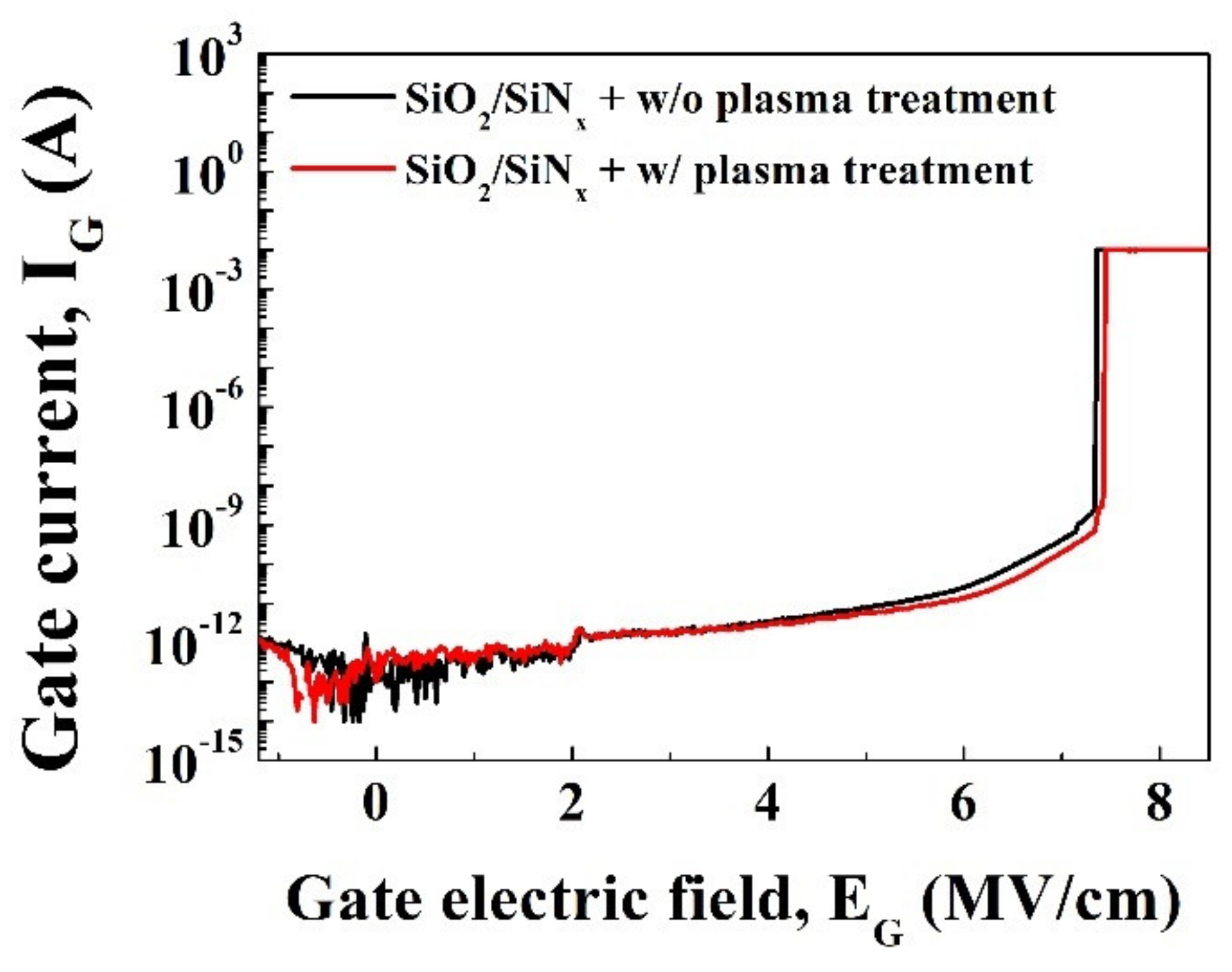
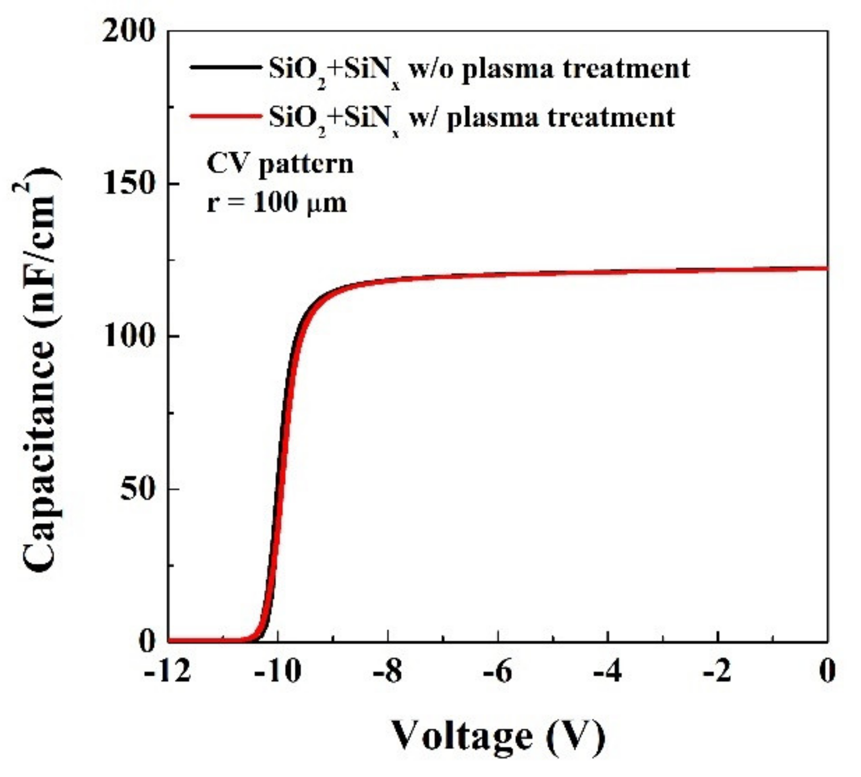
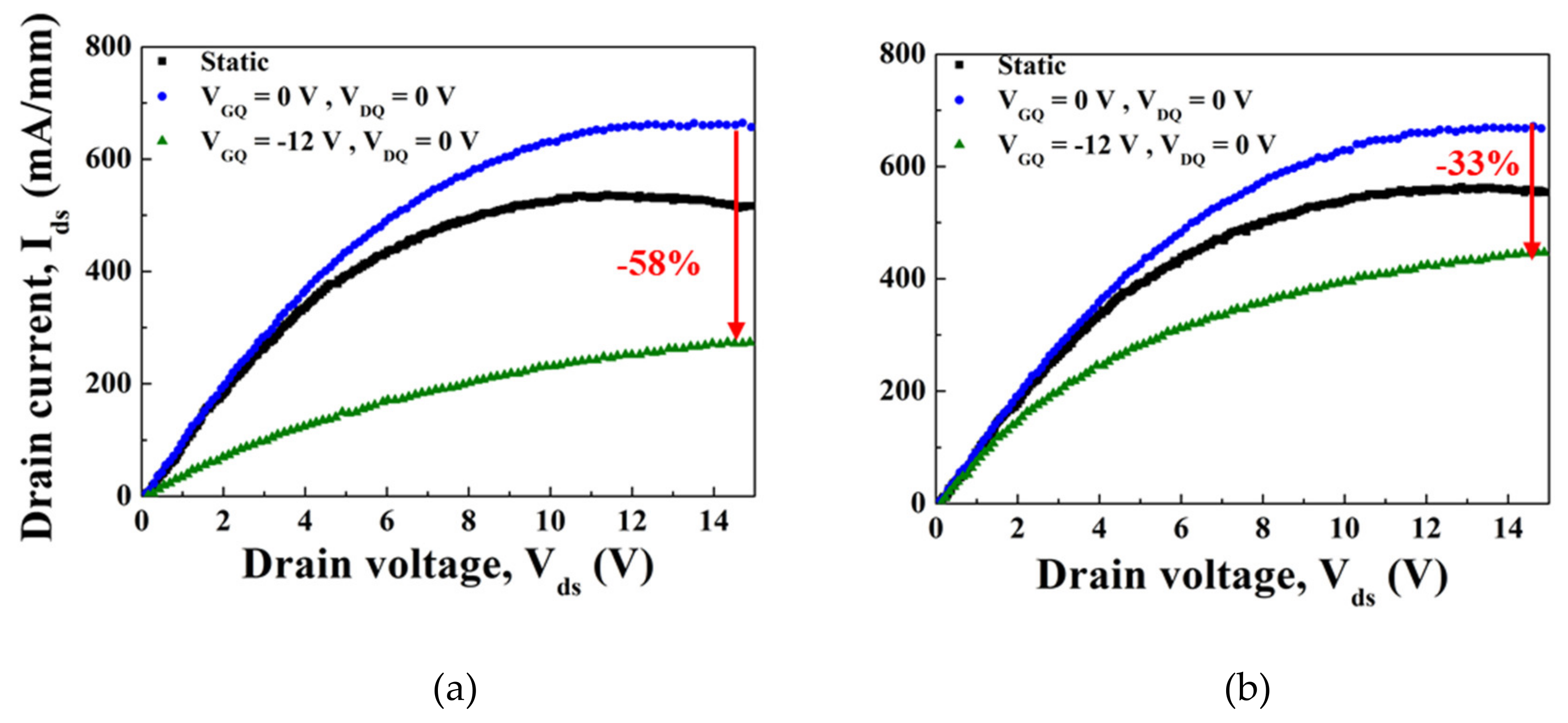
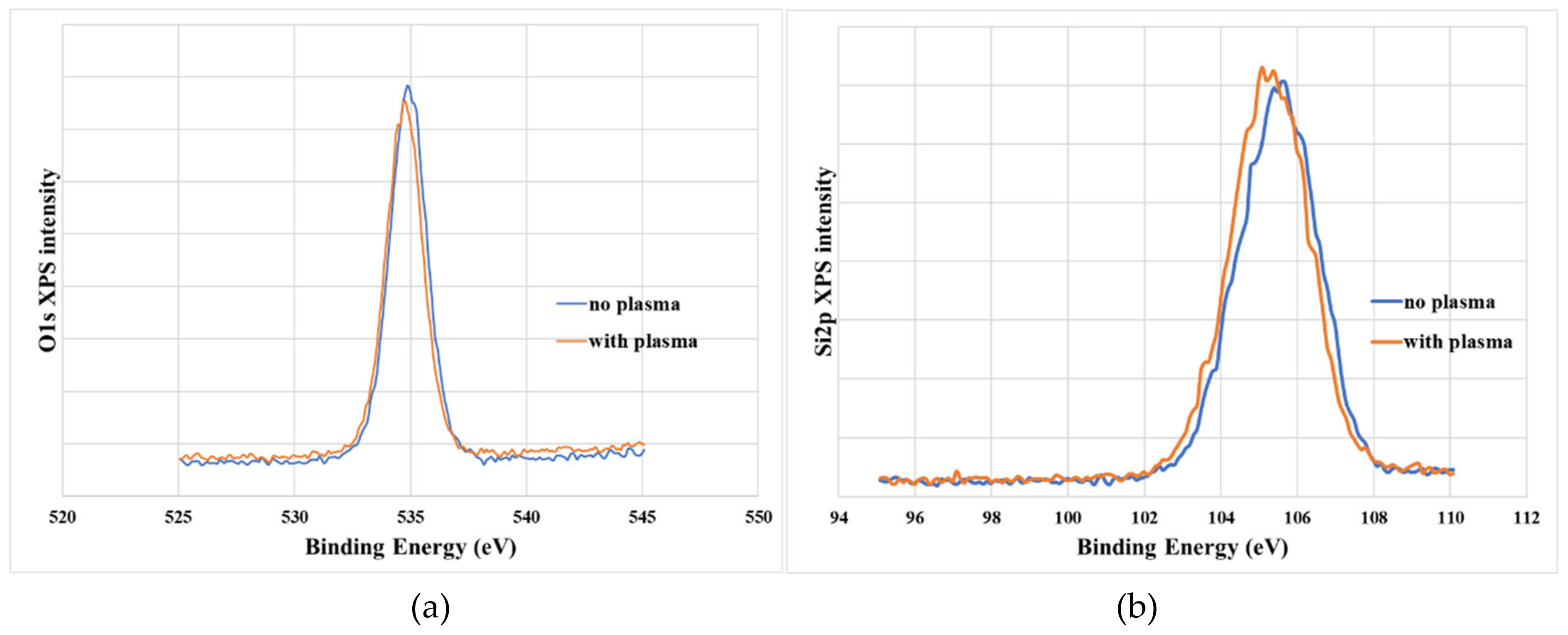
As presented in Figure 1, AlGaN/GaN MOSHEMTs were fabricated on commercially available in situ SiN/AlGaN/GaN heterostructures grown on 6 in silicon substrates by MOCVD. The epilayers, from bottom to top, consist of a 4.5 μm GaN buffer, a 490 nm unintentionally doped GaN channel layer, a 22 nm Al0.25Ga0.75N barrier, a 4 nm GaN cap, and a 10 nm in situ SiN cap. The layer structure information was provided by the wafer provider, Enkris Semiconductor Inc. in Suzhou, China. The Hall mobility (μ) and sheet carrier concentration (nsh) of the 2DEG channel at heterojunction was 1890 cm2/V·s and 8.85 × 10¹², respectively. Circular-type MOS capacitors were also fabricated on the same sample. The device fabrication was done at Inter-university Semiconductor Research Center in Seoul National University, Korea. It started with a recess etching of the AlGaN barrier through in situ SiN to reduce a contact resistance [recess]. A Ti/Al/Ni/Au metal stack (20/120/25/50 nm) was deposited by e-beam evaporation for source/drain electrodes. The ohmic contacts were alloyed by rapid thermal annealing at 830 ℃ for 30 s in N2. Device isolation was performed using mesa formation with a depth of 300 nm. The surface was submitted to oxygen plasma treatment using a microwave asher with 50 W power and 40 sccm flow rate for 2 min, before SiO2 deposition. Following that, a 20 nm PECVD SiO2 layer was deposited for gate insulation and device passivation. Finally, an Ni/Au-based metal stack (20/200 nm) was deposited to form the gate and probe pad. The average ohmic contact resistance was determined to be 0.85 Ω-mm, and the sheet resistance of 2-DEG was ~470 Ω/sq, as measured by the transfer length method (TLM) after the fabrication was complete. Gate length and width of the MOSHEMT were 2 and 100 μm, respectively.

3. Results

Transfer I-V characteristics of the fabricated devices were measured at room temperature by Agilent 4155 semiconductor parameter analyzer. As shown in Figure 2a, oxygen plasma treatment did not change device characteristics including on-current, a threshold voltage (Vth) and transconductance. Figure 2b shows that neither gate leakage current nor subthreshold swing was degraded by plasma treatment. Time-zero-breakdown characteristics were also evaluated to compare the integrity of the gate oxide and did not show significant differences between the two samples, as given in Figure 3.
C-V characteristics were measured at f = 1 MHz from a circular-shaped C-V pattern with radius = 100 um using Agilent B1500A. Figure 4 shows negligible differences in C-V characteristics between two types of devices with or without plasma treatment. This suggests that the dielectric thickness and constant were not altered by the plasma treatment.
Pulsed I-V measurement is a useful tool in analyzing gate lag or drain lag phenomenon caused by the trapping effect [13]. Gate lag characteristics have a strong correlation with RF output performance, which can be improved significantly by minimizing gate lag, i.e., the dispersion between DC and pulsed I-V characteristics [14]. The virtual gate effect, proposed by Vetury et al. [15], is well-known as an origin of the dispersion. Gate lag measurement was performed to investigate the effect of plasma treatment on the trapping phenomenon observed in GaN-based HEMTs by using the Accent DiVA D265 Dynamic analyzer. Quiescent bias points for the two pulsed measurements were VG = VD = 0 V and VG = −12, VD = 0 V. The pulse width was 1 μs with 1 ms of the pulse period. VGQ = −12 V was chosen to ensure that the DUT was completely pinched off and electrons were easily injected from the gate into the traps nearby. Figure 5 shows the pulsed and static I-V characteristics and the difference between static and pulsed I-V. (VG = VD = 0 V) resulted from the self-heating effect. As shown in Figure 5, the MOSHEMT without oxygen plasma treatment exhibited a larger I–V dispersion between the two measurement conditions. Although 38% dispersion was observed in the plasma-treated device, the untreated device showed 58% dispersion at VD = 15 V. This result suggests a more serious virtual gate effect [15] and the ineffectiveness of the suppression of current collapse in the devices without plasma treatment.

4. Discussion

When AlGaN/GaN MOS-HEMTs were treated by oxygen plasma before SiO2 dielectric deposition, they did not show any changes in DC I-V and C-V characteristics, such as pinch-off voltage, transconductance and Cmax, indicating 2DEG property was not altered. Channel and Gate leakage characteristics were not degraded, either.
However, pulsed I-V measurement revealed that gate lag was aggravated if the surface of in situ SiN was not exposed to oxygen plasma before SiO2 deposition. To investigate how the trap states of a SiO2/SiN/AlGaN MOS structure can be modified by oxygen plasma treatment, the devices were submitted to a short-term stress test and ΔVth was monitored. The ΔVth value can easily be translated into an interface trap density using the oxide capacitance [16]. In Figure 6, a plasma-treated device showed ΔVth less than that of an untreated one during the bias stress, with the same electric field and time, suggesting that the interface trap density was decreased by plasma treatment.
We carried out further analysis of the SiO2/SiN/AlGaN MOS structure to understand the origin of the reduced trapping observed from the oxygen–plasma treated device. To quantify the oxygen composition in the SiO2 film, x-ray photoelectron spectroscopy (XPS) measurements with sputter etch treatment was performed with the thetaprobe XPS system from Thermo Fisher Scientific at Analytical Instrumentation Center of Hanyang University, Seoul, Korea. A monochromatic Al Κα X-ray source with 1486.6 eV and sputtering ion gun with Ar+ at 2 keV were used for analysis. At the top surface with no sputter etching, Si 2p and O 1s peak positions (not shown in Figure) are determined to be 103.08 and 532.58 eV for the untreated sample, respectively. Only a little change in binding energy was observed in the plasma-treated sample, showing each peak at 103.48 and 532.98 eV. Figure 7 also presents Si 2p and O 1s peaks, with 150 s of sputter etch time which is suggested to give a depth near the interface between ex-situ SiO2 and in situ SiN. No significant changes in the XPS spectrum were observed. However, the XPS depth profile of each element in Figure 8 reveals that SiO2 on in-situ SiN with oxygen–plasma treatment has an O/Si ratio close to the theoretical value (2:1). This suggests that oxygen–plasma treatment modified the surface of in-situ SiN in favor of the following SiO2 deposition. Plasma oxidation of PECVD and LPCVD nitride has been already demonstrated to produce oxynitride films [17,18] Oxygen–plasma was also applied to convert the surface of silicon nitride into oxide [19]. Buiu et al. proposed that this conversion was due to a loss of nitrogen into the plasma caused by the bonding instability of nitrogen at the surface of the dielectric [20]. Several reports proposed similar mechanisms that weakly bind nitrogen at the surface of silicon nitride can be replaced by oxygen [19,21]. The oxidized surface of silicon nitride by oxygen plasma can probably provide better conditions for ex-situ deposition of SiO2.
The current work is aimed at optimizing the treatment process with varying power and oxygen flow to further improve the SiO2/SiN interface property. A more detailed characterization of the plasma-treated surface before SiO2 deposition is now in progress. Besides, the effects of plasma treatment on the chemical bonding and morphology of the dielectrics will accompany this.

5. Conclusions

We investigate the effect of oxygen–plasma treatment on in-situ SiN on AlGaN/GaN heterojunction for MOS gate devices. Oxygen–plasma treatment was performed before a SiO2 gate insulator was deposited on in situ SiN by PECVD. Oxygen–plasma treatment did not change DC I-V characteristics. However, the dispersion between DC and pulsed I-V characteristics was significantly alleviated by the plasma treatment. Accordingly, the plasma-treated device exhibited a smaller Vth shift than the untreated one, suggesting that the trapping into the interface states was mitigated. The XPS result revealed that the SiO2 layer on the plasma-treated sample exhibited an O/Si ratio much closer to the theoretical value than the untreated one. In cases where a SiO2 layer is employed as a gate insulator on an AlGaN/GaN-on-Si platform with an in situ SiN capping layer, oxygen plasma treatment on the in situ SiN layer can improve the quality of SiO2 significantly.

Author Contributions

Conceptualization, H.K. and G.C.; methodology, H.K. and H.-y.C.; formal analysis, H.K. and G.C.; investigation, G.C.; data curation, G.C.; writing—original draft preparation, G.C.; writing—review and editing, H.K.; visualization, G.H.; supervision, H.K.; funding acquisition, H.K.

Funding

This work was supported by Korea Electric Power Corporation(R18XA06-05) and National Research Foundation of Korea government (NRF-2019R1H1A2078240).

Conflicts of Interest

The authors declare no conflict of interest.

References

  1. Chen, K.J.; Zhou, C. Enhancement-mode AlGaN/GaN HEMT and MIS-HEMT technology. Phys. Status Solidi A 2011, 208, 434–438. [Google Scholar] [CrossRef]
  2. Choi, W.; Ryu, H.; Jeon, N.; Lee, M.; Cha, H.-Y.; Seo, K.-S. Improvement of Vth instability in normally-off GaN MIS-HEMTs employing PEALD-SiNx as an interfacial layer. IEEE Electron Device Lett. 2014, 35, 30–32. [Google Scholar] [CrossRef]
  3. Scott, M.J.; Fu, L.; Zhang, X.; Li, J.; Yao, C.; Sievers, M.; Wang, J. Merits of gallium nitride based power conversion. Semicond. Sci. Technol. 2013, 28, 074013. [Google Scholar] [CrossRef]
  4. Freedsman, J.J. Normally-OFF Al2O3/AlGaN/GaN MOS-HEMT on 8 in. Si with low leakage current and high breakdown voltage (825 V). Appl. Phys. Exp. 2014, 7, 041003. [Google Scholar] [CrossRef]
  5. Huang, T.; Zhu, X.; Wong, K.M.; Lau, K.M. Low-leakage current AlN/GaN MOSHFETs using Al2O3 for increased 2DEG. IEEE Electron Device Lett. 2012, 33, 212–214. [Google Scholar] [CrossRef]
  6. Wu, T.-L. Time dependent dielectric breakdown (TDDB) evaluation of PE-ALD SiN gate dielectrics on AlGaN/GaN recessed gate D-mode MIS-HEMTs and E-mode MIS-FETs. In Proceedings of the IEEE International Reliability Physics Symposium, Monterey, CA, USA, 19–23 April 2015. [Google Scholar]
  7. Derluym, J.; Boeykens, S.; Cheng, K.; Vandersmissen, R.; Das, J.; Ruythooren, W.; Degroote, S.; Leys, M.R.; Germain, M.; Borghs, G. Improvement of AlGaN/GaN high electron mobility transistor structures by in situ deposition of a Si3N4 surface layer. J. Appl. Phys. 2005, 98, 054501. [Google Scholar] [CrossRef]
  8. Lu, X.; Ma, J.; Jiang, H.; Liu, C.; Lau, K.M. Low trap states in situ SiNx/AlN/GaN metal-insulator-semiconductor structures grown by metal-organic chemical vapor deposition. Appl. Phys. Lett. 2014, 105, 102911–102913. [Google Scholar] [CrossRef]
  9. Tadjer, M.J.; Anderson, T.J.; Hobart, K.D.; Mastro, M.A.; Hite, J.K.; Caldwell, J.D.; Picard, Y.N.; Kub, F.J.; Eddy, C.R. Electrical and Optical Characterization of AlGaN/GaN HEMTs with In Situ and Ex-situ Deposited SiN x Layers. J. Electron. Mater. 2010, 39, 2452–2458. [Google Scholar] [CrossRef]
  10. Kambayashi, H.; Nomura, T.; Kato, S.; Ueda, H.; Teramoto, A.; Sugawa, S.; Ohmi, T. High integrity SiO2 gate insulator formed by microwave excited plasma enhanced chemical vapor deposition for AlGaN/GaN hybrid metal–oxide–semiconductor heterojunction field-effect transistor on Si substrate. Jpn. J. Appl. Phys. 2012, 51, 04DF03. [Google Scholar] [CrossRef]
  11. Adivarahan, V.; Rai, S.; Tipirneni, N.; Koudymov, A.; Yang, J.; Simin, G.; Khan, M.A. Digital oxide deposition of SiO2 layers for III-nitride metal–oxide–semiconductor heterostructure field-effect transistors. Appl. Phys. Lett. 2006, 88, 182507. [Google Scholar] [CrossRef]
  12. Park, B.-R.; Lee, J.-G.; Choi, W.; Kim, H.; Seo, K.-S.; Cha, H.-Y. High Quality ICPCVD SiO2 for Normally-off AlGaN/GaN-on-Si Recessed MOSHFETs. IEEE Electron Dev. Lett. 2013, 34, 354–356. [Google Scholar] [CrossRef]
  13. Binari, S.C.; Ikossi, K.; Roussos, J.A.; Kruppa, W.; Park, D.; Dietrich, H.B.; Koleske, D.D.; Wichenden, A.E.; Henry, R.L. Trapping Effects and Microwave Power Performance in AlGaN/GaN HEMTs. IEEE Trans. Electron Devices 2001, 48, 465–471. [Google Scholar] [CrossRef]
  14. Green, B.M.; Chu, K.K.; Chumbes, J.A.; Smart, J.A.; Shealy, J.R.; Eastman, L.E. The effect of surface passivation on the microwave characteristics of undoped AlGaN/GaN HEMTs. IEEE Electron. Dev. Lett. 2000, 21, 268–270. [Google Scholar] [CrossRef]
  15. Vetury, R.; Zhang, N.Q.; Keller, S.; Mishra, U.K. The impact of surface states on the DC and RF characteristics of AlGaN/GaN HFETs. IEEE Trans. Electron Devices 2001, 48, 560–566. [Google Scholar] [CrossRef]
  16. Lagger, P.; Ostermaier, C.; Pobegen, G.; Pogany, D. Towards understanding the origin of threshold voltage instability of AlGaN/GaN MISHEMTs. In Proceedings of the International Electron Devices Meeting (IEDM), San Francisco, CA, USA, 10–13 December 2012. [Google Scholar]
  17. Goswami, R.; Butcher, J.B.; Ginige, R.; Zhang, J.F.; Taylor, S.; Eccleston, W. Low temperature gate dielectrics formed by plasma anodization of silicon nitride. Electron. Lett. 1988, 24, 129–1270. [Google Scholar] [CrossRef]
  18. Kennedy, G.P.; Taylor, S.; Eccleston, W.; Arnoldbik, W.M.; Habraken, F.H.P.M. Physical and electrical characterisation of oxynitride films produced by plasma oxidation of deposited silicon nitride. Microelectron. Eng. 1995, 28, 141–144. [Google Scholar] [CrossRef]
  19. Usenko, A.; Senawiratne, J. Silicon nitride surface conversion into oxide to enable hydrophilic bonding. ECS Trans. 2010, 33, 475–483. [Google Scholar]
  20. Buiu, O.; Kennedy, G.P.; Gartner, M.; Taylor, S. Structural analysis of silicon dioxide and silicon oxynitride films produced using an oxygen plasma. IEEE Trans. Plasma Sci. 1998, 26, 1700–1712. [Google Scholar] [CrossRef]
  21. Jiminez, C.; Perriere, J.; Vickridge, I.; Enard, J.P.; Albella, J.M. Transformation of silicon nitride in oxygen plasma. Surf. Coat. Tech. 1991, 45, 147–154. [Google Scholar] [CrossRef]
Figure 1. Cross-sectional diagram of in situ SiN/AlGaN/GaN metal–organic semiconductor high electron mobility transistor (MOS-HEMT) on Si (not scaled).
Materials 12 03968 g001
Figure 2. (a) Transfer I-V characteristics measured at VD = 1 and 10 V. (b) Subthreshold (solid mark) and gate leakage (open mark) characteristics measured at VD = 1 and 10 V.
Materials 12 03968 g002
Figure 3. Time-zero-breakdown characteristics of SiO2/in situ SiN/AlGaN/GaN MOS structure.
Materials 12 03968 g003
Figure 4. C-V characteristics of SiO2/in situ SiN/AlGaN/GaN MOS capacitor measured at 1 MHz.
Materials 12 03968 g004
Figure 5. Pulsed I-V (gate lag) characteristics measured with 1 us-VG pulsed width in a 0.1 % duty cycle. (a) Without plasma treatment (b) With plasma treatment.
Materials 12 03968 g005
Figure 6. ΔVth induced by a short-term gate bias stress measured from the plasma-treated and non-treated device.
Materials 12 03968 g006
Figure 7. XPS spectrum of O1s and Si2p in the vicinity of the SiO2/SiN interface. Sputter etching for 150 s. (a) O1s (b) Si2p.
Materials 12 03968 g007
Figure 8. Atomic percent ratio vs. sputter time SiO2/in situ SiN/AlGaN MOS structure. (a) Without plasma treatment (b) With plasma treatment.
Materials 12 03968 g008

