Application-Specific Oxide-Based and Metal–Dielectric Thin-Film Materials Prepared by Radio Frequency Magnetron Sputtering


Abstract
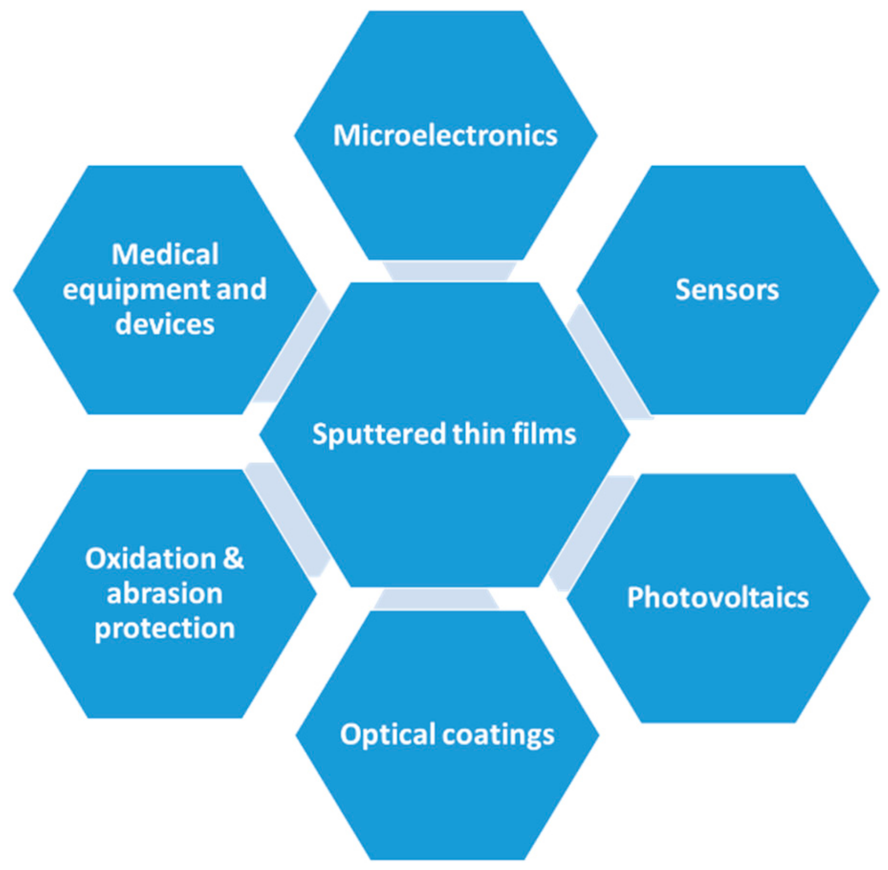
1. Introduction
2. Garnets, Garnet-Oxide Composites, and Multilayer Structures Deposited by Sputtering
2.1. Deposition Process Parameters for Growing Bi-Substituted Iron Garnets, GOC Precursor Layers, and GOC-Based Multilayer Structures
2.2. Optical Properties and MO Performance of Bi-Substituted Iron Garnets, GOC Single Layers, and MO Performance of GOC-Based Multilayer Structures
3. Ruthenium Oxide Thin-Films Grown on Flexible and Rigid Substrates for Cost-Effective Sensor Electrodes
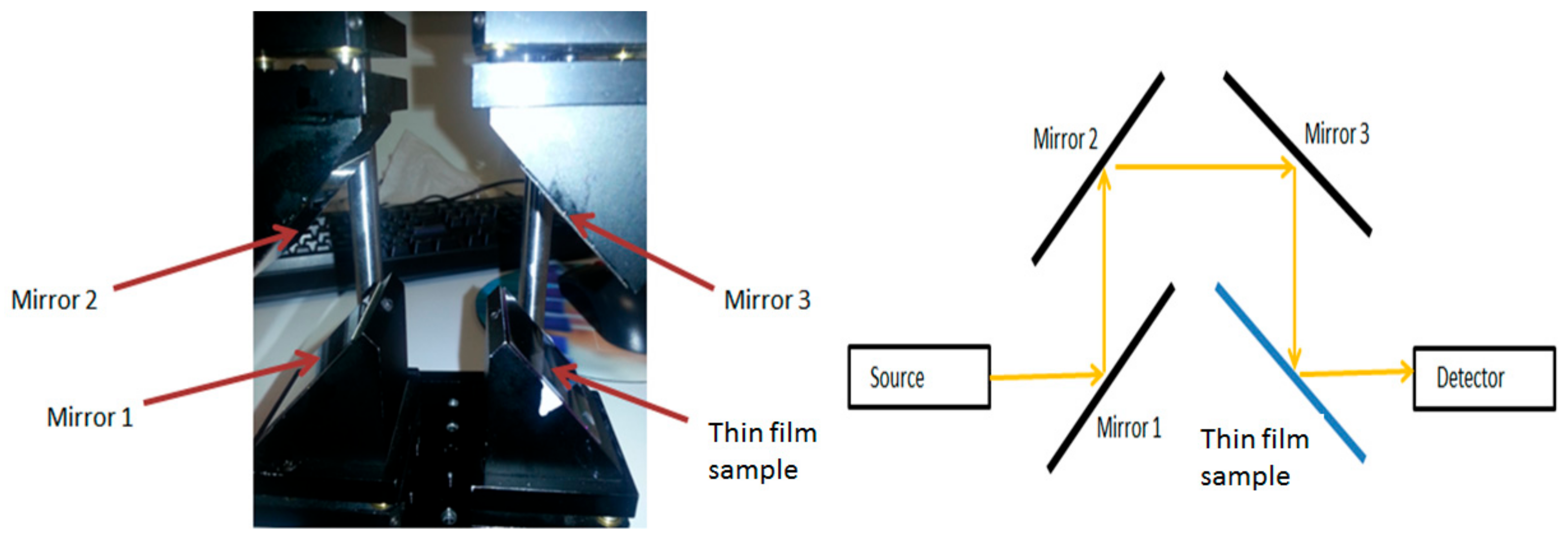
3.1. Experimental
3.2. Results and Comparison
4. Metal–Dielectric Nanocomposite-Based Multilayer Building Blocks for Transparent Solar and Thermal Regulation Coatings
4.1. Deposition of MDC Layers and Multilayer Structures
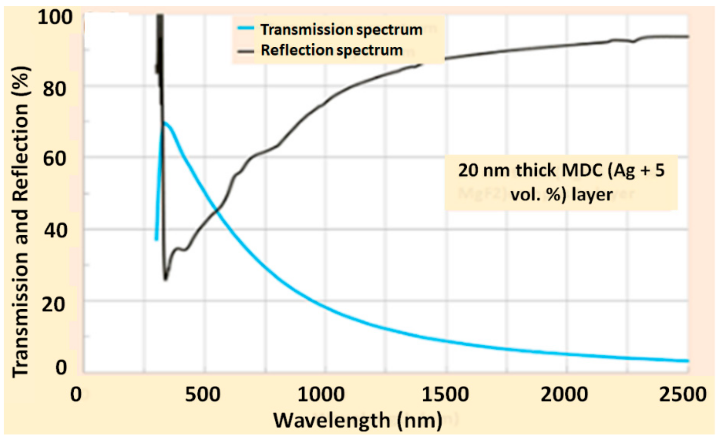
4.2. Optical Characteristics of MDC Thin Films and MDC-Containing Multilayer Structures
5. Conclusions
Author Contributions
Funding
Acknowledgments
Conflicts of Interest
References
- Grove, W.R. On the electro-chemical polarity of gases. Philos. Trans. R. Soc. 1852, 142, 87–101. [Google Scholar] [CrossRef][Green Version]
- Wright, A.W. On the production of transparent metallic films by the electrical discharge in exhausted tubes. Am. J. Sci. Arts 1877, 13, 49–55. [Google Scholar] [CrossRef]
- Greene, J.E. Review Article: Tracing the recorded history of thin-film sputter deposition: From the 1800s to 2017. J. Vac. Sci. Technol. A 2017, 35, 05C204-1-60. [Google Scholar] [CrossRef]
- Lakhtakia, A.; Messier, R. Nanoengineered Morphology and Optics; SPIE-The International Society for Optical Engineering: Bellingham, WA, USA, 2005; Chapter 2; pp. 27–48. [Google Scholar]
- Alfonso, E.; Olaya, J.; Cubillos, G. Thin Film Growth through Sputtering Technique and Its Applications. Available online: https://www.intechopen.com/books/crystallization-science-and-technology/thin-film-growth-through-sputtering-technique-and-its-applications (accessed on 21 October 2019).
- Mattox, D.M. A Short History: Magnetron Sputtering Deposition. Available online: https://www.svc.org/DigitalLibrary/documents/2015_Summer_DMM.pdf (accessed on 21 October 2019).
- Depla, D.; Mahieu, S.; Greene, J.E. Sputter Deposition Processes. Available online: https://core.ac.uk/download/pdf/55744819.pdf (accessed on 21 October 2019).
- Anders, A.; Mattox, D.M. Magnetron Sputtering: An Unfinished Journey, Tutorial presentation. In Proceedings of the 58th Annual Technical Conference of the Society of Vacuum Coaters, Santa Clara, CA, USA, 25–30 April 2015; Available online: www.svc.org (accessed on 21 October 2019).
- Mattox, D.M. The Foundations of Vacuum Coating Technology; William Andrew: Oxford, UK; Cambridge, MA, USA, 2018. [Google Scholar]
- Sarkar, J. Sputtering Materials for VLSI and Thin Film Devices; William Andrew: Norwich, NY, USA, 2010; ISBN 978-0-8155-1593-7. [Google Scholar]
- Lu, D.X.; Wong, E.M.W.; Pun, E.Y.B.; Chung, P.S.; Jia, G.C. PZT thin films by radio frequency magnetron sputtering. In Applications of Photonic Technology 2; Lampropoulos, G.A., Lessard, R.A., Eds.; Springer: Boston, MA, USA, 2013. [Google Scholar] [CrossRef]
- Lin, K.T.; Wu, J.M. RF-magnetron sputtering of Titanium dioxide for microelectronics applications. J. Appl. Phys. 2004, 43, 232–236. [Google Scholar] [CrossRef]
- Sakthivel, P.; Murugan, R.; Asaithambi, S.; Murugesan, K.; Rajendran, R.; Ravi, G. Radio frequency magnetron sputtered CdO thin films for optoelectronic applications. J. Phys. Chem. Solids 2018, 126, 1–10. [Google Scholar] [CrossRef]
- Singh, J.; Khan, S.A.; Shah, J.; Kotnala, R.K.; Mohapatra, S. Nanostructured TiO2 thin films prepared by RF magnetron sputtering for photocatalytic applications. Appl. Surf. Sci. 2017, 422, 953–961. [Google Scholar] [CrossRef]
- Pisarkiewicz, T.; Maziarz, W.; Rydosz, A.; Jankowski, H.; Sokulski, J. Deposition of nanocrystalline WO3 thin film using magnetron sputtered multilayer structure in view of gas sensor applications. In Proceedings of the IMCS 2012—The 14th International Meeting on Chemical Sensors, Nuremberg, Germany, 20–23 May 2012. [Google Scholar] [CrossRef]
- Lee, S.; Kim, J.Y.; Lee, T.W.; Kim, W.K.; Kim, B.S.; Park, J.H.; Bae, J.S.; Cho, Y.C.; Kim, J.; Oh, M.W.; et al. Fabrication of high-quality single-crystal Cu thin films using radio-frequency sputtering. Sci. Rep. 2014, 4, 6230. [Google Scholar] [CrossRef] [PubMed]
- Maurya, D.; Sardarinejad, A.; Alameh, K. Recent development in R. F. magnetron sputtered thin films for pH sensing applications-An overview. Coatings 2014, 4, 756–771. [Google Scholar] [CrossRef]
- Surmenev, R.; Vladescu, A.; Surmeneva, M.; Ivanova, A.; Braic, M.; Grubova, I.; Cotrut, C.M. Radio frequency magnetron sputter deposition as a tool for surface modification of medical implants, modern technologies for creating the thin-film systems and coatings. IntechOpen 2017. [Google Scholar] [CrossRef]
- Saikumar, A.K.; Nehate, S.D.; Sundaram, K. Review-RF sputtered films of Gd2O3. ECS J. Solid State Sci. Technol. 2019, 8, Q3064–Q3078. [Google Scholar] [CrossRef]
- Prosolov, K.A.; Popova, K.S.; Belyavskaya, O.A.; Rau, J.V.; Gross, K.A.; Ubelis, A.; Sharkeev, Y.P. RF magnetron-sputtered coatings deposited from biphasic calcium phosphate targets for biomedical implant applications. Bioact. Mater. 2017, 2, 170–176. [Google Scholar] [CrossRef] [PubMed]
- D’Heurle, F.M. Aluminum films deposited by rf sputtering. Metall. Mater. Trans. B 1970, 1, 725–732. [Google Scholar] [CrossRef]
- Kay, E.; Parmigiani, F.; Parrish, W. Microstructure of sputtered metal films grown in high- and low-pressure discharges. J. Vac. Sci. Technol. 1988, A6, 3074. [Google Scholar] [CrossRef]
- Rydosz, A.; Brudnik, A.; Staszek, K. Metal oxide thin films prepared by magnetron sputtering technology for volatile organic compound detection in the microwave frequency range. Materials 2019, 12, 877. [Google Scholar] [CrossRef] [PubMed]
- Verger, F.; Nazabal, V.; Colas, F.; Němec, P.; Cardinaud, C.; Baudet, E.; Chahal, R.; Rinnert, E.; Boukerma, K.; Peron, I.; et al. RF sputtered amorphous chalcogenide thin films for surface enhanced infrared absorption spectroscopy. Opt. Mat. Exp. 2013, 3, 2112–2131. [Google Scholar] [CrossRef]
- Lee, H.; Huang, Y.T.; Horn, M.W.; Feng, S.P. Engineered optical and electrical performance of rf–sputtered undoped nickel oxide thin films for inverted perovskite solar cells. Sci. Rep. 2018, 8, 5590. [Google Scholar] [CrossRef] [PubMed]
- Lee, J.C.; Kang, K.H.; Kim, S.K.; Park, I.J.; Song, J.; Yoon, K.H. Direct deposition of textured ZnO:Al TCO films by rf sputtering method for thin film solar cells. In Proceedings of the Conference Record of the Twenty-Ninth IEEE Photovoltaic Specialists Conference, New Orleans, LA, USA, 19–24 May 2002. [Google Scholar] [CrossRef]
- Sanal, K.C.; Morales, R.B.; Castrejón, O.L.; Nairz, P.K.; Nair, M.T.S. Thin Film Zn-Mg-Al-O Produced by r. f. sputtering used in antimony sulfide solar cells. J. Electrochem. Soc 2019, 166, H3119–H3124. [Google Scholar] [CrossRef]
- Jaydeep, S.; Yadav, S.; Malla, B.P.; Kulkarni, A.R.; Venkatramani, N. Growth and dielectric behavior of radio frequency magnetron-sputtered lead magnesium niobate thin films. Appl. Phys. Lett. 2002, 81, 3840–3842. [Google Scholar] [CrossRef]
- Lee, N.Y.; Sekine, T.; Ito, Y.; Uchino, K. Deposition profile of RF-magnetron-sputtered BaTiO3 thin films. J. Appl. Phys. 1994, 33, 1484–1488. [Google Scholar] [CrossRef]
- Bobrowski, A.; Królicka, A.; Śliwa, J.; Zarębski, J.; Januś, M.; Kyzioł, K. PVD fabrication of lead film electrodes and their catalytic adsorptive stripping voltammetric performance in the presence of oxidants. Electrochem. Commun. 2018, 94, 49–54. [Google Scholar] [CrossRef]
- Hishmeh, G.A.; Barr, T.L.; Sklyarov, A.; Hardcastle, S. Thin polymer films prepared by radio frequency plasma sputtering of polytetrafluoroethylene and polyetherimide targets. J. Vac. Sci. Technol. A Vac. Surf. Films 1996, 14, 1330–1338. [Google Scholar] [CrossRef]
- Kylián, O.; Shelemin, A.; Solař, P.; Pleskunov, P.; Nikitin, D.; Kuzminova, A.; Štefaníková, R.; Kúš, P.; Cieslar, M.; Hanuš, J.; et al. Magnetron Sputtering of Polymeric Targets: From Thin Films to Heterogeneous Metal/Plasma. Materials 2019, 12, 2366. [Google Scholar] [CrossRef] [PubMed]
- Stelmashuk, V.; Biederman, H.; Slavínská, D.; Trchová, M.; Hlidek, P. Rf magnetron sputtering of polypropylene. Vacuum 2004, 75, 207–215. [Google Scholar] [CrossRef]
- Hanus, J.; Kousal, J.; Choukourov, A.; Biederman, H.; Slavinska, D. RF magnetron sputtering of poly(propylene) in a mixture of argon and nitrogen. Plasma Process. Polym. 2007, 4, 806–811. [Google Scholar] [CrossRef]
- Zubar, T.I.; Sharko, S.A.; Tishkevich, D.I.; Kovaleva, N.N.; Vinnik, D.A.; Gudkova, S.A.; Trukhanova, E.L.; Trofimov, E.A.; Chizhik, S.A.; Panina, L.V.; et al. Anomalies in Ni-Fe nanogranular films growth. J. Alloys Comps. 2018, 748, 970–978. [Google Scholar] [CrossRef]
- Xie, T.; Fu, L.; Gao, B.; Zhu, J.; Yang, W.; Li, D.; Zhou, L. The crystallization character of W-Cu thin films at the early stage of deposition. Thin Solid Films 2019, 690, 137555. [Google Scholar] [CrossRef]
- Stognij, A.I.; Sharko, S.A.; Serokurova, A.I.; Trukhanov, S.V.; Trukhanov, A.V.; Panina, L.V.; Ketsko, V.A.; Dyakonov, V.P.; Szymczak, H.; Vinnik, D.A.; et al. Preparation and investigation of the magnetoelectric properties in layered cermet structures. Ceram. Int. 2019, 45, 13030–13036. [Google Scholar] [CrossRef]
- Available online: https://www.prnewswire.com/news-releases/sputtering-targets-and-sputtered-films-technology-and-markets-300418821.html (accessed on 20 February 2019).
- Available online: https://www.marketwatch.com/press-release/thin-film-materials-market-is-expected-to-witness-a-substantial-growth-from-2018-to-2024-2018-10-12 (accessed on 24 March 2019).
- Geller, S. Crystal chemistry of garnets. Z. Kristallographie 1967, 125, 1–47. [Google Scholar] [CrossRef]
- Novak, A.; Gibbs, G.V. The crystal chemistry of the silicate garnets. Am. Miner. 1971, 56, 791–825. [Google Scholar]
- Zvezdin, A.K.; Kotov, V.A. Modern Magnetooptics and Magnetooptical Materials; Institute of Physics Publishing: Bristol, UK; Philadelphia, PA, USA, 1997; ISBN 075030362X. [Google Scholar]
- Buhrer, C.F. Faraday rotation and dichroism of bismuth calcium vanadium iron garnet. J. Appl. Phys. 1969, 40, 4500. [Google Scholar] [CrossRef]
- Freiser, M.J. A survey of magnetooptic effects. IEEE. Trans. Mag. 1968, 4, 152–161. [Google Scholar] [CrossRef]
- Scott, G.B.; Lacklison, D.E. Magnetooptic properties and applications of Bismuth substituted iron garnets. IEEE Trans. Magn. 1976, 12, 292–311. [Google Scholar] [CrossRef]
- Taketoshi, H.; Yukio, M.; Junichiro, N. Growth and characterization of Liquid-Phase Epitaxial Bi-Substituted iron garnet films for magneto-optic application. Jpn. J. Appl. Phys. 1985, 24, 1316. [Google Scholar]
- Huang, M.; Zhang, S. A new Bi-substituted rare-earth iron garnet for a wideband and temperature-stabilized optical isolator. J. Mater. Res. 2000, 15, 1665–1668. [Google Scholar] [CrossRef]
- Anoikin, E.V.; Sides, P.J. Plasma-activated chemical vapor deposition of Bismuth-substituted iron garnets for magneto-optical data storage. IEEE Trans. Magn. 1995, 31, 3239–3241. [Google Scholar] [CrossRef]
- Syvorotka, I.M.; Ubizskii, S.B.; Kucera, M.; Kuhn, M.; Vertesy, Z. Growth and characterization of Bi, Prand Bi, Sc-substituted lutetium iron garnet films with planar magnetization for magneto-optic visualization. J. Phys. D Appl. Phys. 2001, 34, 1178–1187. [Google Scholar] [CrossRef]
- Kahl, S.; Grishin, A.M.; Kharstev, S.I.; Kawano, K.; Abell, J.S. Bi3Fe5O12 thin film visulaizer. IEEE Trans. Mag. 2001, 3, 2457–2459. [Google Scholar] [CrossRef]
- Levy, M. The on-chip integration of magnetooptic waveguide isolators. IEEE Quantum Electron. 2002, 8, 1300–1306. [Google Scholar] [CrossRef]
- Khartsev, S.I.; Grishin, A.M. [Bi3Fe5O12/Gd3Ga5O12]m magneto-optical photonic crystals. Appl. Phys. Lett. 2005, 87, 122504. [Google Scholar] [CrossRef]
- Kang, S.; Yin, S.; Adyam, V.; Li, Q.; Zhu, Y. Bi3Fe4Ga1O12 garnet properties and its application to ultrafast switching in the visible spectrum. IEEE Trans. Magn. 2007, 43, 3656–3660. [Google Scholar] [CrossRef]
- Drezdzon, S.M.; Yoshie, T. On-chip waveguide isolator based on bismuth iron garnet operating via nonreciprocal single-mode cutoff. Opt. Express 2009, 17, 9276–9281. [Google Scholar] [CrossRef] [PubMed]
- Nur-E-Alam, M.; Vasiliev, M.; Alameh, K.; Valli, C. Magneto-optical visualisation for high-resolution forensic data recovery using advanced thin film nano-materials. In Proceedings of the International Cyber Resilience (SECAU 2010), Perth, WA, Australia, 23–24 August 2010; pp. 78–82. [Google Scholar]
- Bi, L.; Hu, J.; Jiang, P.; Kim, H.S.; Kim, D.H.; Onbasli, M.C.; Dionne, F.F.; Ross, C.A. Magneto-optical thin films for on-chip monolithic integration of non-reciprocal photonic devices. Materials 2013, 6, 5094–5117. [Google Scholar] [CrossRef] [PubMed]
- Belotelov, V.I.; Kreilkamp, L.E.; Akimov, I.A.; Kalish, A.N.; Bykov, D.A.; Kasture, S.; Yallapragada, V.J.; Gopal, A.V.; Grishin, A.M.; Khartsev, S.I.; et al. Plasmon mediated magneto-optical transparency. Nat. Commun. 2013, 4, 2128. [Google Scholar] [CrossRef] [PubMed]
- Kuz’michev, A.N.; Kreilkamp, L.E.; Nur-E-Alam, M.; Bezus, E.; Vasiliev, M.; Akimov, I.A.; Alameh, K.; Bayer, M.; Belotelov, V.I. Tunable optical nanocavity of iron-garnet with a buried metal layer. Materials 2015, 8, 3012–3023. [Google Scholar] [CrossRef]
- Du, Q.; Fakhrul, T.; Zhang, Y.; Hu, J.; Ross, C.A. Monolithic magneto-optical oxide thin films for on-chip optical isolation. MRS Bull. 2018, 43, 413–418. [Google Scholar] [CrossRef]
- Krumme, J.P.; Doormann, V.; Willich, J. Bismuth iron garnet films prepared by rf magnetron sputtering. J. Appl. Phys. 1985, 57, 3885–3887. [Google Scholar] [CrossRef]
- Yamaga, M.; Yusa, K.; Miyazaki, Y. Optical waveguide of Nd-Doped garnet thin film RF-sputtered on Y3Al5O12 substrate. Jpn. J. Appl. Phys. 1986, 25, 194–199. [Google Scholar] [CrossRef]
- Ostoréro, J.; Escorne, M.; Pecheron-Guegan, A. Dy3Fe5O12 garnet thin films grown from sputtering of metallic targets. J. Appl. Phys. 1994, 75, 6103. [Google Scholar] [CrossRef]
- Park, M.B.; Cho, N.H. Structural and magnetic characteristics of yttrium iron garnet (YIG, Ce: YIG) films prepared by RF magnetron sputter techniques. J. Magn. Magn. Mater. 2001, 231, 253–264. [Google Scholar] [CrossRef]
- Boudiar, T.; Payet-Gervy, B.; Blanc-Mignon, M.F.; Rousseau, J.J.; Berre, M.L.; Joisten, H. Magneto-optical properties of yttrium iron garnet (YIG) thin films elaborated by radio frequency sputtering. J. Magn. Magn. Mater. 2004, 284, 77–85. [Google Scholar] [CrossRef]
- Gomi, M.; Tanida, T.; Abe, M. RF sputtering of highly Bi-substituted garnet films on glass substrates for magneto-optic memory. J. Appl. Phys. 1985, 57, 3888–3890. [Google Scholar] [CrossRef]
- Challeton, D.; Bechevet, B.; Rolland, B.; Armand, M.F. RF sputtering of Bi-substituted garnet films for magneto-optic memory. J. Magn. Magn. Mater. 1990, 83, 37–38. [Google Scholar] [CrossRef]
- Deng, Y.; Fowlkes, J.D.; Rack, P.D.; Fitz-Gerald, J.M. Thin film rf magnetron sputtering of gadolinium-doped yttrium aluminum garnet ultraviolet emitting materials. Opt. Mater. 2006, 29, 183–191. [Google Scholar] [CrossRef]
- Lobe, S.; Dellen, C.; Finsterbusch, M.; Gehrke, H.G.; Sebold, D.; Tsai, C.L.; Uhlenbruck, S.; Guillon, O. Radio frequency magnetron sputtering of Li7La3Zr2O12 thin films for solid-state batteries. J. Power Sour. 2016, 307, 684–689. [Google Scholar] [CrossRef]
- Bhoi, B.; Venkataramani, N.; Aiyar, R.P.R.C.; Prasad, S.; Kostylev, M. Effect of annealing on the structural and FMR properties of epitaxial YIG thin films grown by RF magnetron sputtering. IEEE. Trans. Magn. 2018, 54. [Google Scholar] [CrossRef]
- Vasiliev, M.; Nur-E-Alam, M.; Kotov, V.A.; Alameh, K.; Belotelov, V.I.; Burkov, V.I.; Zvezdin, A.K. RF magnetron sputtered (BiDy)3(FeGa)5O12:Bi2O3 composite materials possessing record magneto-optic quality in the visible spectral region. Opt. Express 2009, 17, 19519–19535. [Google Scholar] [CrossRef]
- Vasiliev, M.; Nur-E-Alam, M.; Perumal, P.; Kotov, V.A.; Alameh, K.; Lee, Y.T.; Lee, Y.P. Annealing behavior and crystal structure of RF-sputtered bi-substituted dysprosium iron garnet films having excess co-sputtered bi-oxide content. J. Phys. D Appl. Phys. 2011, 44, 075002. [Google Scholar] [CrossRef]
- Nur-E-Alam, M.; Vasiliev, M.; Kotov, V.A.; Alameh, K. Highly bismuth-substituted, record-performance magneto-optic garnet materials with low coercivity for applications in integrated optics, photonic crystals, imaging and sensing. Opt. Mater. Express 2011, 1, 413–427. [Google Scholar] [CrossRef]
- Nur-E-Alam, M.; Vasiliev, M.; Alameh, K. Bi3Fe5O12: Dy2O3 composite thin film materials for magneto-photonics and magneto-plasmonics. Opt. Mater. Express 2014, 4, 1866–1875. [Google Scholar] [CrossRef]
- Nur-E-Alam, M.; Vasiliev, M.; Alameh, K.; Kotov, V.A.; Demidov, V.; Balabanov, D. YIG: Bi2O3 nanocomposite thin films for magneto-optic and microwave applications. J. Nanomater. 2015, 182691. [Google Scholar] [CrossRef]
- Nur-E-Alam, M.; Vasiliev, M.; Alameh, K. High-performance RF-sputtered Bi-substituted iron garnet thin films with almost in-plane magnetization. Opt. Mater. Express 2017, 7, 676–686. [Google Scholar] [CrossRef]
- Kotov, V.A.; Shavrov, V.G.; Popkov, A.F.; Vasiliev, M.; Alameh, K.; Nur-E-Alam, M.; Alyabyeva, L.N.; Balabanov, D.E.; Burkov, V.I.; Virchenko, M.K. Magneto-optic properties of ultrathin nanocrystalline ferrite garnet films in the 8K to 300K temperature interval. J. Nanomater. 2018, 7605620. [Google Scholar] [CrossRef]
- Nur-E-Alam, M.; Vasiliev, M.; Belotelov, V.; Alameh, K. Properties of ferrite garnet (Bi, Lu, Y)3(Fe, Ga)5O12 thin film materials prepared by RF magnetron sputtering. Nanomaterials 2018, 8, 355. [Google Scholar] [CrossRef] [PubMed]
- Swanepoel, R. Determination of the thickness and optical constants of amorphous silicon. J. Phys. E Sci. Instrum. 1983, 16, 1214–1222. [Google Scholar] [CrossRef]
- Vasiliev, M.; Alameh, K.; Nur-E-Alam, M. Analysis, optimization, and characterization of magnetic photonic crystal structures and thin-film material layers. Technologies 2019, 7, 49. [Google Scholar] [CrossRef]
- Nur-E-Alam, M.; Vasiliev, M.; Kotov, V.A.; Balavanov, D.E.; Akimov, I.A.; Alameh, K. Properties of exchange coupled all-garnet magneto-optic thin film multilayer structures. Materials 2015, 8, 1976–1992. [Google Scholar] [CrossRef]
- Rabeh, M.B.; Touatti, R.; Kanzari, M. Substrate temperature effects on structural optical and electrical properties of vacuum evaporated Cu2ZnSnS4 thin films. Int. J. Eng. Pract. Res. 2013, 2, 71–76. [Google Scholar]
- Yang, Q.; Zhang, H.; Wen, Q.; Liu, Y.J. Effects of off-stoichiometry and density on the magnetic and magneto-optical properties of yttrium iron garnet films by magnetron sputtering method. Appl. Phys. 2010, 108, 073901. [Google Scholar] [CrossRef]
- Jiang, M.C.; Wu, T.B. The effect of electrode composition on rf magnetron sputtering deposition of Pb[(Mg1/3Nb2/3)0.7Ti0.3]O3 films. J. Mater. Res. 1994, 9, 1879–1886. [Google Scholar] [CrossRef]
- Park, J.Y.; Heo, J.K.; Kang, Y.C. The properties of RF sputtered Zirconium oxide thin films at different plasma gas ratio. Bull. Korean Chem. Soc. 2010, 31, 397–400. [Google Scholar] [CrossRef]
- Hamada, K.; Ogawa, T.; Okumura, H.; Ishihara, K.N. The effect of substrate roughness on the properties of RF sputtered AZO thin film. MRS Commun. 2019, 9, 697–701. [Google Scholar] [CrossRef]
- Ghorannevis, Z.; Akbarnejad, E.; Ghoranneviss, M. Effects of various deposition times and RF powers on CdTe thin film growth using magnetron sputtering. J. Theor. Appl. Phys. 2016, 10, 225–231. [Google Scholar] [CrossRef]
- Reddy, Y.K.V.; Mergel, D. Structural and electrical properties of RuO2 thin films prepared by rf-magnetron sputtering and annealing at different temperatures. J. Mater. Sci. Mater. Electron. 2006, 17, 1029–1034. [Google Scholar] [CrossRef]
- Tien, C.L.; Lin, H.Y.; Chang, C.K.; Tang, C.J. Effect of oxygen flow rate on the optical, electrical, and mechanical properties of dc sputtering ITO thin films. Adv. Condens. Matter Phys. 2018, 2647282. [Google Scholar] [CrossRef]
- Haque, F.; Rahman, K.S.; Islam, M.A.; Rashid, M.J.; Akhtaruzzaman, M.; Alam, M.M.; Alothman, Z.A.; Sopian, K.; Amin, N. Growth optimization of ZnS thin films by RF magnetron sputtering as prospective buffer layer in thin film solar cells. Chalcogenide Lett. 2014, 11, 189–197. [Google Scholar]
- Tehranchi, M.M.; Hamidi, S.M.; Hasanpour, A.; Mozaffari, M.; Amighian, J. The effect of target rotation rate on structural and morphological properties of thin garnet films fabricated by pulsed laser deposition. Opt. Laser Technol. 2011, 43, 609–612. [Google Scholar] [CrossRef]
- Lonsdale, W. Development, Manufacture and Application of a Solid-State pH Sensor Using Ruthenium Oxide. Ph.D. Thesis, Edith Cowan University, Perth, WA, Australia, 2018. Available online: https://ro.ecu.edu.au/theses/2095 (accessed on 21 October 2019).
- Stradiotto, N.R.; Yamanaka, H.; Zanoni, M.V.B. Review electrochemical sensors: A powerful tool in analytical chemistry. J. Braz. Chem. Soc. 2003, 14, 159–173. [Google Scholar] [CrossRef]
- Lonsdale, W.; Shylendra, S.P.; Brouwer, S.; Wajrak, M.; Alameh, K. Application of ruthenium oxide pH sensitive electrode to samples with high redox interference. Sens. Actuators B Chem. 2018, 273, 1222–1225. [Google Scholar] [CrossRef]
- Bat’ko, I.; Flachbatt, K. Design of RuO2-based thermometers the millikelvin temperature range. Cryogenics 1995, 35, 105–108. [Google Scholar] [CrossRef]
- Brischwein, M.; Grothe, H.; Wiest, J.; Zottmann, M.; Ressler, J.; Wolf, B. Planar Ruthenium Oxide sensors for Cell-on-a-Chip metabolic studies. Chem. Analityczna 2009, 54, 1193–1201. [Google Scholar]
- Mohelnikova, J. Materials for reflective coatings of window glass applications. Constr. Build. Mater. 2009, 23, 1993–1998. [Google Scholar] [CrossRef]
- Al-Kuhaili, M.F.; Al-Aswad, A.H.; Durrani, S.M.A.; Bakhtiari, I.A. Energy-saving transparent heat mirrors based on tungsten oxide-gold WO3/Au/WO3 multilayer structures. Sol. Energy 2012, 86, 3183–3189. [Google Scholar] [CrossRef]
- Kanu, S.S.; Binions, R. Thin films for solar control applications. Proc. R. Soc. Math. Phys. Eng. Sci. 2010, 466, 19–44. [Google Scholar] [CrossRef]
- Mouedden, Y.E.; Alghamedi, R.; Nur-E-Alam, M.; Vasiliev, M.; Alameh, K. Thin film coatings for solar and thermal radiation control prepared by physical vapour deposition. In Proceedings of the International Conference on High-Capacity Optical Networks and Enabling Technologies Conference 2012, HONET 2012, Istanbul, Turkey, 12–14 December 2012. [Google Scholar]
- Chen, W.; Thoreson, M.D.; Kildishev, A.V.; Shalaev, V.M. Ultra-Thin Ultra-Smooth and Low Loss Silver and Silver-Silica Composite Films for Superlensing Applications. Available online: https://engineering.purdue.edu/~shalaev/Publication_list_files/QThE4.pdf (accessed on 21 October 2019).
- Anders, A.; Byon, E.; Kim, D.; Fukuda, K.; Lim, S.H.N. Smoothing of ultrathin silver films by transition metal seeding. Solid State Commun. 2006, 140, 225–229. [Google Scholar] [CrossRef]
- Yu, B.; Leung, K.M.; Guo, Q.; Lau, W.M.; Yang, J. Synthesis of Ag–TiO2 composite nano thin film for antimicrobial application. Nanotechnology 2011, 22, 115603. [Google Scholar] [CrossRef]
- Cummings, K.D.; Garland, J.C.; Tanner, D.B. Optical properties of a small-particle composite. Phys. Rev. B 1984, 30, 4170–4182. [Google Scholar] [CrossRef]
- Nielsen, R.B.; Thoreson, M.D.; Chen, W.; Kristensen, A.; Hvam, J.M.; Shalaev, V.M.; Boltasseva, A. Toward superlensing with metal–dielectric composites and multilayers. Appl. Phys. B 2010, 100, 93–100. [Google Scholar] [CrossRef]
- Amin, K.A.M.; Panhuis, M. Reinforced materials based on chitosan, TiO2 and Ag composites. Polymers 2012, 4, 590–599. [Google Scholar] [CrossRef]
- Chiang, H.P.; Leung, P.T.; Tse, W.S. Optical properties of composite materials at high temperatures. Solid State Commun. 1997, 101, 45–50. [Google Scholar] [CrossRef]
- Nur-E-Alam, M.; Vasiliev, M.; Alameh, K. Energy Saving Coating Materials: Design, Process, Implementation and Recent Developments; Elsevier: Amsterdam, The Netherlands, 2019. Chapter 4. (In Press)
- Vasiliev, M.; Nur-E-Alam, M.; Alameh, K. Initial field testing results from building-integrated solar energy harvesting windows installation in Perth, Australia. Appl. Sci. 2019, 9, 4002. [Google Scholar] [CrossRef]
- Vasiliev, M.; Nur-E-Alam, M.; Alameh, K. Recent developments in solar energy-harvesting technologies for building integration and distributed energy generation. Energies 2019, 12, 1080. [Google Scholar] [CrossRef]
- Lee, J.H.; Lee, S.H.; Hwangbo, C.K. Optical and structural properties of TiO2/Ti/Ag/TiO2 and TiO2/ITO/Ag/ITO/TiO2 metal-dielectric multilayers by RF magnetron sputtering for display application. J. Korean Phys. Soc. 2001, 44, 750–756. [Google Scholar]
- Liu, X.; Cai, X.; Mao, J.; Jin, C. ZnS/Ag/ZnS nano-multilayer films for transparent electrodes in flat display application. Appl. Surf. Sci. 2001, 183, 103–110. [Google Scholar] [CrossRef]


| Process Parameters | Layer Structure (Bi-Substituted Iron Garnet and Garnet-Oxide (Single) Layer) | Layer Structure (GOC-Based All-Garnet Multilayers) |
|---|---|---|
| Sputtering targets | Bi2Dy1Fe4Ga1O12 and Bi2O3 | Bi2Dy1Fe4Ga1O12, Bi1.8Lu1.2Fe3.6Al1.4O12 and Bi2O3 |
| Radio frequency (RF) power | Bi2Dy1Fe4Ga1O12 (150–300 W), and Bi2O3 (40–150 W) | Bi2Dy1Fe4Ga1O12 (300 W), Bi2O3 (60 W), and Bi1.8Lu1.2Fe3.6Al1.4O12 (170 W) |
| Base pressure (Torr) | <3 × 10⁻⁶–5 × 10⁻⁶ | <3 × 10⁻⁶–5 × 10⁻⁶ |
| Process gas | Ar | Ar |
| Process pressure | 2–3 mTorr | 2–3 mTorr |
| Target-to-substrate distance (cm) | ~18 | ~18 |
| Substrate stage rotation rate (rpm) | 15–16 | 15–16 |
| Substrate temperature (°C) | Room temperature | Room temperature |
| Process Parameters | Layer Structure (Single Layer MDC) | Layer Structure (Multilayers Containing MDC Layer) |
|---|---|---|
| Sputtering targets | Ag, MgF2 | Al2O3, Zr2O3, Ag, MgF2 |
| RF Power | Ag (55–65 W), MgF2 (83–95 W) | Al2O3 (190–195 W), Ag (55–65 W), MgF2 (83–95 W) |
| Base pressure (Torr) | 5 × 10⁻⁶ | 5 × 10⁻⁶ |
| Process gas | Ar | Ar |
| Process pressure | 2–3 mTorr | 1–3 mTorr |
| Substrate temperature (°C) | Room temperature | Room temperature |
| Post deposition heat treatment | No | Up to 500 °C for 1–10 h |
© 2019 by the authors. Licensee MDPI, Basel, Switzerland. This article is an open access article distributed under the terms and conditions of the Creative Commons Attribution (CC BY) license (http://creativecommons.org/licenses/by/4.0/).
Share and Cite
Nur-E-Alam, M.; Lonsdale, W.; Vasiliev, M.; Alameh, K. Application-Specific Oxide-Based and Metal–Dielectric Thin-Film Materials Prepared by Radio Frequency Magnetron Sputtering. Materials 2019, 12, 3448. https://doi.org/10.3390/ma12203448
Nur-E-Alam M, Lonsdale W, Vasiliev M, Alameh K. Application-Specific Oxide-Based and Metal–Dielectric Thin-Film Materials Prepared by Radio Frequency Magnetron Sputtering. Materials. 2019; 12(20):3448. https://doi.org/10.3390/ma12203448
Chicago/Turabian StyleNur-E-Alam, Mohammad, Wade Lonsdale, Mikhail Vasiliev, and Kamal Alameh. 2019. "Application-Specific Oxide-Based and Metal–Dielectric Thin-Film Materials Prepared by Radio Frequency Magnetron Sputtering" Materials 12, no. 20: 3448. https://doi.org/10.3390/ma12203448
APA StyleNur-E-Alam, M., Lonsdale, W., Vasiliev, M., & Alameh, K. (2019). Application-Specific Oxide-Based and Metal–Dielectric Thin-Film Materials Prepared by Radio Frequency Magnetron Sputtering. Materials, 12(20), 3448. https://doi.org/10.3390/ma12203448