A Review of Perovskite Photovoltaic Materials’ Synthesis and Applications via Chemical Vapor Deposition Method


Abstract
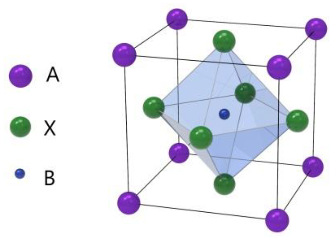
1. Introduction
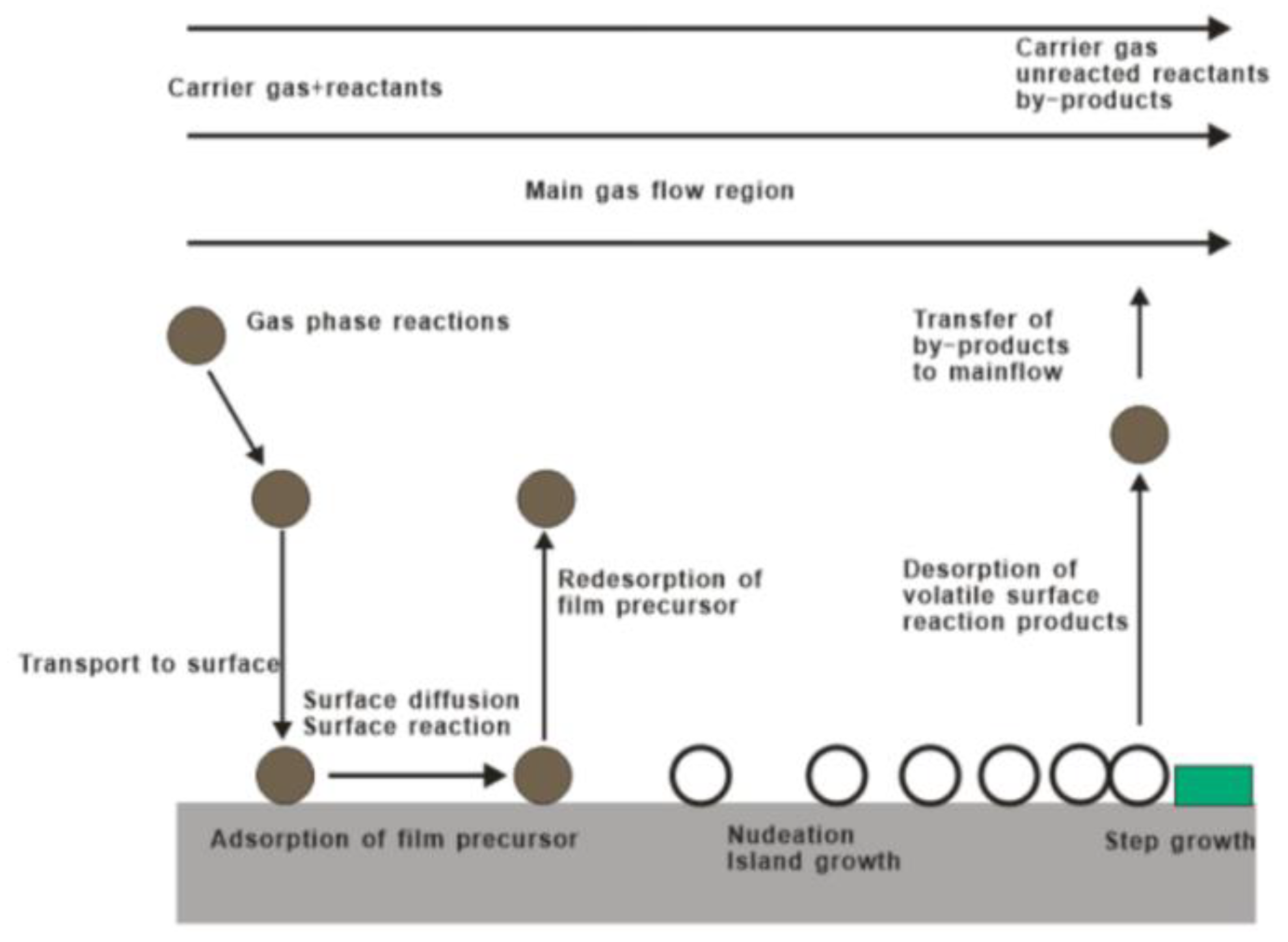
2. CVD Method
3. Synthesis and Application of PPMs Using the CVD Methods
3.1. Perovskite Photovoltaic Film Synthesis through a Variety of CVD Technologies
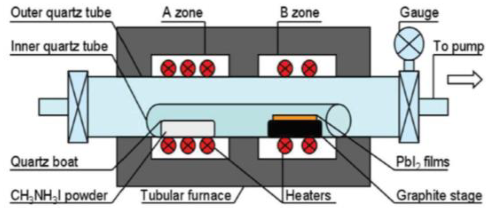
3.1.1. Atmospheric Pressure and Low Pressure CVD (APCVD and LPCVD) Method
3.1.2. Aerosol Assisted CVD (AACVD) Method
3.1.3. Hybrid Physical CVD (HPCVD) Method
3.2. Low Dimensional Perovskite Photovoltaic Materials Synthesized by CVD Technologies
4. Electrode, Window, Blocking and Electron Transport Layer Materials of Perovskite Devices Prepared by CVD Technologies
4.1. APCVD Method
4.2. PECVD Method
4.3. Pulsed CVD Method
4.4. Physical Chemical Vapor Deposition (PCVD) Method
4.5. AACVD Method
5. Conclusions and Future Outlook
Author Contributions
Funding
Acknowledgments
Conflicts of Interest
References
- Rose, G. Beschreibung einiger neuen Mineralien des Urals. Ann. Phys. 1839, 124, 551–573. [Google Scholar] [CrossRef]
- Liu, M.Z.; Johnston, M.B.; Snaith, H.J. Efficient planar heterojunction perovskite solar cells by vapour deposition. Nature 2013, 501, 395–398. [Google Scholar] [CrossRef] [PubMed]
- Lee, M.M.; Teuscher, J.; Miyasaka, T.; Murakami, T.N.; Snaith, H.J. Efficient hybrid solar cells based on meso-superstructured organometal halide perovskites. Science 2012, 338, 643–647. [Google Scholar] [CrossRef] [PubMed]
- Stranks, S.D.; Eperon, G.E.; Grancini, G.; Menelaou, C.; Alcocer, M.J.; Leijtens, T.; Herz, L.M.; Petrozza, A.; Snaith, H.J. Electron-hole diffusion lengths exceeding 1 micrometer in an organometal trihalide perovskite absorber. Science 2013, 342, 341–344. [Google Scholar] [CrossRef] [PubMed]
- Liu, D.; Kelly, T.L. Perovskite solar cells with a planar heterojunction structure prepared using room-temperature solution processing techniques. Nat. Photonics 2014, 8, 133–138. [Google Scholar] [CrossRef]
- Jang, D.M.; Park, K.; Kim, D.H.; Park, J.; Shojaei, F.; Kang, H.S.; Ahn, J.P.; Lee, J.W.; Song, J.K. Reversible halide exchange reaction of organometal trihalide perovskite colloidal nanocrystals for full-range band gap tuning. Nano Lett. 2015, 15, 5191–5199. [Google Scholar] [CrossRef]
- Dong, R.; Fang, Y.; Chae, J.; Dai, J.; Xiao, Z.; Dong, Q.; Yuan, Y.; Centrone, A.; Zeng, X.C.; Huang, J. High-gain and low-driving-voltage photodetectors based on organolead triiodide perovskites. Adv. Mater. 2015, 27, 1912–1918. [Google Scholar] [CrossRef]
- Veldhuis, S.A.; Boix, P.P.; Yantara, N.; Li, M.; Sum, T.C.; Mathews, N.; Mhaisalkar, S.G. Perovskite materials for light-emitting diodes and lasers. Adv. Mater. 2016, 28, 6804–6834. [Google Scholar] [CrossRef]
- Shan, Q.S.; Song, J.Z.; Zou, Y.S.; Li, J.H.; Xu, L.M.; Xue, J.; Dong, Y.H.; Han, B.N.; Chen, J.W.; Zeng, H.B. High performance metal halide perovskite light-emitting diode: From material design to device optimization. Small 2017, 13. [Google Scholar] [CrossRef]
- Ha, S.T.; Su, R.; Xing, J.; Zhang, Q.; Xiong, Q.H. Metal halide perovskite nanomaterials: Synthesis and applications. Chem. Sci. 2017, 8, 2522–2536. [Google Scholar] [CrossRef]
- Makarov, S.; Furasova, A.; Tiguntseva, E.; Hemmetter, A.; Berestennikov, A.; Pushkarev, A.; Zakhidov, A.; Kivshar, Y. Halide-perovskite resonant nanophotonics. Adv. Opt. Mater. 2019, 7. [Google Scholar] [CrossRef]
- Dong, Q.; Fang, Y.; Shao, Y.; Mulligan, P.; Qiu, J.; Cao, L.; Huang, J. Electron-hole diffusion lengths > 75 μm in solution-grown CH3NH3PbI3 single crystals. Science 2015, 347, 967–970. [Google Scholar] [CrossRef] [PubMed]
- Nie, W.; Tsai, H.; Asadpour, R.; Blancon, J.C.; Neukirch, A.J.; Gupta, G.; Crochet, J.J.; Chhowalla, M.; Tretiak, S.; Alam, M.A.; et al. High-efficiency solution-processed perovskite solar cells with millimeter-scale grains. Science 2015, 347, 522–525. [Google Scholar] [CrossRef]
- Xiao, Z.; Bi, C.; Shao, Y.; Dong, Q.; Wang, Q.; Yuan, Y.; Wang, C.; Gao, Y.; Huang, J. Efficient, high yield perovskite photovoltaic devices grown by interdiffusion of solution-processed precursor stacking layers. Energy Environ. Sci. 2014, 7, 2619–2623. [Google Scholar] [CrossRef]
- Ning, Z.; Gong, X.; Comin, R.; Walters, G.; Fan, F.; Voznyy, O.; Yassitepe, E.; Buin, A.; Hoogland, S.; Sargent, E.H. Quantum-dot-in-perovskite solids. Nature 2015, 523, 324–341. [Google Scholar] [CrossRef]
- Deng, W.; Xu, X.Z.; Zhang, X.J.; Zhang, Y.D.; Jin, X.C.; Wang, L.; Lee, S.T.; Jie, J.S. Organometal halide perovskite quantum dot light-emitting diodes. Adv. Funct. Mater. 2016, 26, 4797–4802. [Google Scholar] [CrossRef]
- Horvath, E.; Spina, M.; Szekrenyes, Z.; Kamaras, K.; Gaal, R.; Gachet, D.; Forro, L. Nanowires of methylammonium lead iodide (CH3NH3PbI3) prepared by low temperature solution-mediated crystallization. Nano Lett. 2014, 14, 6761–6766. [Google Scholar] [CrossRef]
- Petrov, A.A.; Pellet, N.; Seo, J.Y.; Belich, N.A.; Kovalev, D.Y.; Shevelkov, A.V.; Goodilin, E.A.; Zakeeruddin, S.M.; Tarasov, A.B.; Graetzel, M. New insight into the formation of hybrid perovskite nanowires via structure directing adducts. Chem. Mater. 2017, 29, 587–594. [Google Scholar] [CrossRef]
- Liu, P.; He, X.; Ren, J.; Liao, Q.; Yao, J.; Fu, H. Organic–Inorganic hybrid perovskite nanowire laser arrays. ACS Nano 2017, 11, 5766–5773. [Google Scholar] [CrossRef]
- Ha, S.T.; Liu, X.F.; Zhang, Q.; Giovanni, D.; Sum, T.C.; Xiong, Q.H. Synthesis of organic–Inorganic lead halide perovskite nanoplatelets: Towards high-performance perovskite solar cells and optoelectronic devices. Adv. Opt. Mater. 2014, 2, 838–844. [Google Scholar] [CrossRef]
- Liu, J.Y.; Xue, Y.Z.; Wang, Z.Y.; Xu, Z.Q.; Zheng, C.X.; Weber, B.; Song, J.C.; Wang, Y.S.; Lu, Y.R.; Zhang, Y.P.; et al. Two-dimensional CH3NH3PbI3 perovskite: Synthesis and optoelectronic application. ACS Nano 2016, 10, 3536–3542. [Google Scholar] [CrossRef] [PubMed]
- Burschka, J.; Pellet, N.; Moon, S.J.; Humphry-Baker, R.; Gao, P.; Nazeeruddin, M.K.; Grätzel, M. Sequential deposition as a route to high-performance perovskite-sensitized solar cells. Nature 2013, 499, 316–319. [Google Scholar] [CrossRef] [PubMed]
- Zhou, H.P.; Chen, Q.; Li, G.; Luo, S.; Song, T.B.; Duan, H.S.; Hong, Z.R.; You, J.B.; Liu, Y.S.; Yang, Y. Interface engineering of highly efficient perovskite solar cells. Science 2014, 345, 542–546. [Google Scholar] [CrossRef] [PubMed]
- Eperon, G.E.; Burlakov, V.M.; Docampo, P.; Goriely, A.; Snaith, H.J. Morphological control for high performance, solution-processed planar heterojunction perovskite solar cells. Adv. Funct. Mater. 2014, 24, 151–157. [Google Scholar] [CrossRef]
- Dualeh, A.; Tetreault, N.; Moehl, T.; Gao, P.; Nazeeruddin, M.K.; Grätzel, M. Effect of annealing temperature on film morphology of organic–inorganic hybrid perovskite solid-state solar cells. Adv. Funct. Mater. 2014, 24, 3250–3258. [Google Scholar] [CrossRef]
- Xiao, M.; Huang, F.; Huang, W.; Dkhissi, Y.; Zhu, Y.; Etheridge, J.; Weale, A.G.; Bach, U.; Cheng, Y.B.; Spiccia, L. A fast deposition-crystallization procedure for highly efficient lead iodide perovskite thin-film solar cells. Angew. Chem. Int. Ed. 2014, 53, 9898–9903. [Google Scholar] [CrossRef] [PubMed]
- Chen, C.W.; Kang, H.W.; Hsiao, S.Y.; Yang, P.F.; Chiang, K.M.; Lin, H.W. Efficient and uniform planar-type perovskite solar cells by simple sequential vacuum deposition. Adv. Mater. 2014, 246, 6647–6652. [Google Scholar] [CrossRef] [PubMed]
- Longo, G.; Gil-Escrig, L.; Degen, M.J.; Sessolo, M.; Bolink, H.J. Perovskite solar cells prepared by flash evaporation. Chem. Commun. 2015, 51, 7376–7378. [Google Scholar] [CrossRef] [PubMed]
- Deng, Y.; Peng, E.; Shao, Y.; Xiao, Z.; Dong, Q.; Huang, J. Scalable fabrication of efficient organolead trihalide perovskite solar cells with doctor-bladed active layers. Energy Environ. Sci. 2015, 8, 1544–1550. [Google Scholar] [CrossRef]
- Hwang, K.; Jung, Y.S.; Heo, Y.J.; Scholes, F.H.; Watkins, S.E.; Subbiah, J.; Jones, D.J.; Kim, D.Y.; Vak, D. Toward large scale roll-to-roll production of fully printed perovskite solar cells. Adv. Mater. 2015, 27, 1241–1247. [Google Scholar] [CrossRef]
- Barrow, A.T.; Pearson, A.J.; Kwak, C.; Dunbar, A.D.F.; Buckley, A.R.; Lidzey, D.G. Efficient planar heterojunction mixed-halide perovskite solar cells deposited via spray-deposition. Energy Environ. Sci. 2014, 7, 2944–2950. [Google Scholar] [CrossRef]
- Wei, Z.; Chen, H.; Yan, K.; Yang, S. Inkjet printing and instant chemical transformation of a CH3NH3PbI3/nanocarbon electrode and interface for planar perovskite solar cells. Angew. Chem. Int. Ed. 2014, 53, 13239–13243. [Google Scholar] [CrossRef] [PubMed]
- Chen, Q.; Zhou, H.; Hong, Z.; Luo, S.; Duan, H.S.; Wang, H.H.; Liu, Y.; Li, G.; Yang, Y. Planar heterojunction perovskite solar cells via vapor-assisted solution process. J. Am. Chem. Soc. 2014, 136, 622–655. [Google Scholar] [CrossRef] [PubMed]
- Luo, P.F.; Liu, Z.F.; Xia, W.; Yuan, C.C.; Cheng, J.G.; Lu, Y.W. Uniform, stable, and efficient planar-heterojunction perovskite solar cells by facile low-pressure chemical vapor deposition under fully open-air conditions. ACS Appl. Mater. Interfaces 2015, 7, 2708–2714. [Google Scholar] [CrossRef] [PubMed]
- Chen, J.; Zhou, S.; Jin, S.; Li, H.; Zhai, T. Crystal organometal halide perovskites with promising optoelectronic applications. J. Mater. Chem. C 2016, 4, 11–27. [Google Scholar] [CrossRef]
- Ono, L.K.; Leyden, M.R.; Wang, S.; Qi, Y. Organometal halide perovskite thin films and solar cells by vapor deposition. J. Mater. Chem. A 2016, 4, 6693–6713. [Google Scholar] [CrossRef]
- Luo, P.F.; Zhou, S.W.; Xia, W.; Cheng, J.G.; Xu, C.X.; Lu, Y.W. Chemical vapor deposition of perovskites for photovoltaic application. Adv. Mater. Interfaces 2017, 4. [Google Scholar] [CrossRef]
- Xu, X.; Wang, W.; Zhou, W.; Shao, Z. Recent advances in novel nanostructuring methods of perovskite electrocatalysts for energy-related applications. Small Methods 2018, 2. [Google Scholar] [CrossRef]
- Jamal, M.S.; Bashar, M.S.; Hasan, A.M.; Almutairi, Z.A.; Alharbi, H.F.; Alharthi, N.H.; Karim, M.R.; Misran, H.; Amin, N.; Sopian, K.B.; et al. Fabrication techniques and morphological analysis of perovskite absorber layer for high-efficiency perovskite solar cell: A review. Renew. Sustain. Energy Rev. 2018, 98, 469–488. [Google Scholar] [CrossRef]
- Leyden, M.R.; Ono, L.K.; Raga, S.R.; Kato, Y.; Wang, S.; Qi, Y. High performance perovskite solar cells by hybrid chemical vapor deposition. J. Mater. Chem. A 2014, 2, 18742–18745. [Google Scholar] [CrossRef]
- Ting, J.M.; Huang, N.Z. Thickening of chemical vapor deposited carbon fiber. Carbon 2001, 39, 835–839. [Google Scholar] [CrossRef]
- Darr, J.A.; Guo, Z.X.; Raman, V.; Bououdina, M.; Rehman, I.U. Metal organic chemical vapour deposition (MOCVD) of bone mineral like carbonated hydroxyapatite coatings. Chem. Commun. 2004, 6, 696–697. [Google Scholar] [CrossRef] [PubMed]
- Li, Y.; Mann, D.; Rolandi, M.; Kim, W.; Ural, A.; Hung, S.; Javey, A.; Cao, J.; Wang, D.; Yenilmez, E.; et al. Preferential growth of semiconducting single-walled carbon nanotubes by a plasma enhanced CVD method. Nano Lett. 2004, 4, 317–321. [Google Scholar] [CrossRef]
- Suresh, A.; Anastasio, D.; Burkey, D.D. Potential of hexyl acrylate monomer as an initiator in photo-initiated CVD. Chem. Vapor Depos. 2014, 20, 5–7. [Google Scholar] [CrossRef]
- Jones, A.C.; Hitchman, M.L. Chemical Vapour Deposition: Precursors, Processes and Applications; RSC Publishing: London, UK, 2009. [Google Scholar]
- Tavakoli, M.M.; Gu, L.L.; Gao, Y.; Reckmeier, C.; He, J.; Rogach, A.L.; Yao, Y.; Fan, Z.Y. Fabrication of efficient planar perovskite solar cells using a one-step chemical vapor deposition method. Sci. Rep. 2015, 5, 14083. [Google Scholar] [CrossRef] [PubMed]
- Luo, P.F.; Liu, Z.F.; Xia, W.; Yuan, C.C.; Cheng, J.Q.; Xu, C.X.; Lu, Y.W. Chlorine-conducted defect repairmen and seed crystal-mediated vapor growth process for controllable preparation of efficient and stable perovskite solar cells. J. Mater. Chem. A 2015, 3, 22949–22959. [Google Scholar] [CrossRef]
- Leyden, M.R.; Meng, L.Q.; Jiang, Y.; Ono, L.K.; Qiu, L.B.; Juarez-Perez, E.J.; Qin, C.J.; Adachi, C.H.; Qi, Y.B. Methylammonium lead bromide perovskite light-emitting diodes by chemical vapor deposition. J. Phys. Chem. Lett. 2017, 8, 3193–3198. [Google Scholar] [CrossRef] [PubMed]
- Wei, Q.; Bi, H.; Yan, S.; Wang, S.W. Morphology and interface engineering for organic metal halide perovskite-based photovoltaic cells. Adv. Mater. Interfaces 2018, 5. [Google Scholar] [CrossRef]
- Sun, J.C.; Wu, J.; Tong, X.; Wang, Y.N.; Wang, Z.M. Organic/inorganic metal halide perovskite optoelectronic devices beyond solar cells. Adv. Sci. 2018, 5. [Google Scholar] [CrossRef]
- Tavakoli, M.M.; Zakeeruddin, S.M.; Grätzel, M.; Fan, Z.Y. Large-grain tin-rich perovskite films for efficient solar cells via metal alloying technique. Adv. Mater. 2018, 30. [Google Scholar] [CrossRef]
- Swartwout, R.; Hoerantner, M.T.; Bulović, V. Scalable deposition methods for large-area production of perovskite thin films. Energy Environ. Mater. 2019, 2, 119–143. [Google Scholar] [CrossRef]
- Park, N.G. Crystal growth engineering for high efficiency perovskite solar cells. CrystEngComm 2016, 18, 5977–5985. [Google Scholar] [CrossRef]
- Shen, P.S.; Chen, J.S.; Chiang, Y.H.; Li, M.H.; Guo, T.F.; Chen, P. Low-pressure hybrid chemical vapor growth for efficient perovskite solar cells and large-area module. Adv. Mater. Interfaces 2016, 3. [Google Scholar] [CrossRef]
- Leyden, M.R.; Lee, M.V.; Raga, S.R.; Qi, Y.B. Large formamidinium lead trihalide perovskite solar cells using chemical vapor deposition with high reproducibility and tunable chlorine concentrations. J. Mater. Chem. A 2015, 3, 16097–16103. [Google Scholar] [CrossRef]
- Leyden, M.R.; Jiang, Y.; Qi, Y. Chemical vapor deposition grown formamidinium perovskite solar modules with high steady state power and thermal stability. J. Mater. Chem. A 2016, 4, 13125–13132. [Google Scholar] [CrossRef]
- Zhou, Z.M.; Pang, S.P.; Ji, F.X.; Zhang, B.; Cui, G.L. The fabrication of formamidinium lead iodide perovskite thin films via organic cation exchange. Chem. Commun. 2016, 52, 3828–3831. [Google Scholar] [CrossRef] [PubMed]
- Ávila, J.; Momblona, C.; Boix, P.P.; Sessolo, M.; Bolink, H.J. Vapor-deposited perovskites: The route to high-performance solar cell production? Joule 2017, 1, 431–442. [Google Scholar] [CrossRef]
- Wang, Y.P.; Chen, Z.Z.; Deschler, F.; Sun, X.; Lu, T.M.; Wertz, E.A.; Hu, J.M.; Shi, J. Epitaxial halide perovskite lateral double heterostructure. ACS Nano 2017, 11, 3355–3364. [Google Scholar] [CrossRef]
- Tong, G.Q.; Lan, X.Z.; Song, Z.H.; Li, G.P.; Li, H.; Yu, L.W.; Xu, J.; Jiang, Y.; Sheng, Y.; Shi, Y.; et al. Surface-activation modified perovskite crystallization for improving photovoltaic performance. Mater. Today Energy 2017, 5, 173–180. [Google Scholar] [CrossRef]
- Stümmler, D.; Sanders, S.; Pfeiffer, P.; Weingarten, M.; Vescan, A.; Kalisch, H. Direct chemical vapor phase deposition of organometal halide perovskite layers. MRS Adv. 2017, 2, 1189–1194. [Google Scholar] [CrossRef]
- Guo, P.F.; Hossain, M.K.; Shen, X.; Sun, H.B.; Yang, W.C.; Liu, C.P.; Ho, C.Y.; Kwok, C.K.; Tsang, S.W.; Luo, Y.S.; et al. Room-temperature red-green-blue whispering-gallery mode lasing and white-light emission from cesium lead halide perovskite (CsPbX3, X = Cl, Br, I) microstructures. Adv. Opt. Mater. 2018, 6, 1700993. [Google Scholar] [CrossRef]
- Stümmler, D.; Sanders, S.; Pfeiffer, P.; Wickel, N.; Simkus, G.; Heuken, M.; Baumann, P.K.; Vescan, A.; Kalisch, H. Investigation of perovskite solar cells employing chemical vapor deposited methylammonium bismuth iodide layers. MRS Adv. 2018, 3, 3069–3074. [Google Scholar] [CrossRef]
- Lei, Y.; Gu, L.Y.; Yang, X.G.; Zhang, L.L.; Gao, Y.H.; Li, J.X.; Zheng, Z. Fast chemical vapor-solid reaction for synthesizing organometal halide perovskite array thin films for photodetector applications. J. Alloys Compd. 2018, 766, 933–940. [Google Scholar] [CrossRef]
- Tran, V.D.; Pammi, S.V.N.; Dao, V.D.; Choi, H.S.; Yoo, S.G. Chemical vapor deposition in fabrication of robust and highly efficient perovskite solar cells based on single-walled carbon nanotubes counter electrodes. J. Alloys Compd. 2018, 747, 703–711. [Google Scholar] [CrossRef]
- Tian, C.C.; Wang, F.; Wang, Y.P.; Yang, Z.; Chen, X.J.; Mei, J.J.; Liu, H.Z.; Zhao, D.X. Chemical vapor deposition method grown all-inorganic perovskite microcrystals for self-powered photodetectors. ACS Appl. Mater. Interfaces 2019, 11, 15804–15812. [Google Scholar] [CrossRef] [PubMed]
- Stümmler, D.; Sanders, S.; Gerstenberger, F.; Pfeiffer, F.; Simkus, G.; Baumann, P.K.; Heuken, M.; Vescan, M.; Kalisch, H. Reaction engineering of CVD methylammonium bismuth iodide layers for photovoltaic applications. J. Mater. Res. 2019, 34, 608–615. [Google Scholar] [CrossRef]
- Lewis, D.J.; O’Brien, P. Ambient pressure aerosol-assisted chemical vapour deposition of (CH3NH3) PbBr3, an inorganic-organic perovskite important in photovoltaics. Chem. Commun. 2014, 50, 6319–6321. [Google Scholar] [CrossRef]
- Bhachu, D.S.; Scanlon, D.O.; Saban, E.J.; Bronstein, H.; Parkin, I.P.; Carmalt, C.J.; Palgrave, R.G. Scalable route to CH3NH3PbI3 perovskite thin films by aerosol assisted chemical vapour deposition. J. Mater. Chem. A 2015, 3, 9071–9073. [Google Scholar] [CrossRef]
- Afzaal, M.; Yates, H.M. Growth patterns and properties of aerosol-assisted chemical vapor deposition of CH3NH3PbI3 films in a single step. Surf. Coat. Technol. 2017, 321, 336–340. [Google Scholar] [CrossRef]
- Liu, Z.F.; Luo, P.F.; Xia, W.; Zhou, S.W.; Cheng, J.Q.; Sun, L.; Xu, C.X.; Lu, Y.W. Acceleration effect of chlorine in the gas-phase growth process of CH3NH3PbI3(Cl) films for efficient perovskite solar cells. J. Mater. Chem. C 2016, 4, 6336–6344. [Google Scholar] [CrossRef]
- Chen, S.; Briscoe, J.; Shi, Y.; Chen, K.; Wilson, R.M.; Dunn, S.; Binions, R. A simple, low-cost CVD route to high-quality CH3NH3PbI3 perovskite thin films. CrystEngComm 2015, 17, 7486–7489. [Google Scholar] [CrossRef]
- Afzaal, M.; Salhi, B.; Al-Ahmed, A.; Yates, H.; Hakeem, A. Surface-related properties of perovskite CH3NH3PbI3 thin films by aerosol-assisted chemical vapour deposition. J. Mater. Chem. C 2017, 5, 8366–8370. [Google Scholar] [CrossRef]
- Luo, P.F.; Zhou, Y.G.; Zhou, S.W.; Lu, Y.W.; Xu, C.X.; Sun, L. Fast anion-exchange from CsPbI3 to CsPbBr3 via Br2-vapor-assisted deposition for air-stable all-inorganic perovskite solar cells. Chem. Eng. J. 2018, 343, 146–154. [Google Scholar] [CrossRef]
- Peng, Y.; Jing, G.; Cui, T. High crystalline quality perovskite thin films prepared by a novel hybrid evaporation/CVD technique. MRS Online Proc. Libr. Arch. 2015, 1771, 187–192. [Google Scholar] [CrossRef]
- Peng, Y.; Jing, G.; Cui, T. A hybrid physical-chemical deposition process at ultra-low temperatures for high-performance perovskite solar cells. J. Mater. Chem. A 2015, 3, 12436–12442. [Google Scholar] [CrossRef]
- Ioakeimidis, A.; Christodoulou, C.; Lux-Steiner, M.; Fostiropoulos, K. Effect of PbI2 deposition rate on two-step PVD/CVD all-vacuum prepared perovskite. J. Solid State Chem. 2016, 244, 20–24. [Google Scholar] [CrossRef]
- Luo, P.F.; Zhou, S.W.; Liu, Z.F.; Xia, W.; Sun, L.; Cheng, J.G.; Xu, C.X.; Lu, Y.W. A novel transformation route from PbS to CH3NH3PbI3 for fabricating curved and large-area perovskite films. Chem. Commun. 2016, 52, 11203–11206. [Google Scholar] [CrossRef]
- Hossain, M.I.; Qarony, W.; Jovanov, V.; Tsang, Y.H.; Knipp, D. Nanophotonic design of perovskite/silicon tandem solar cells. J. Mater. Chem. A 2018, 6, 3625–3633. [Google Scholar] [CrossRef]
- Jiang, Y.; Leyden, M.R.; Qiu, L.B.; Wang, S.H.; Ono, L.K.; Wu, Z.F.; Juarez-Perez, E.J.; Qi, Y.B. Combination of hybrid CVD and cation exchange for upscaling Cs-substituted mixed cation perovskite solar cells with high efficiency and stability. Adv. Funct. Mater. 2018, 28. [Google Scholar] [CrossRef]
- Zhang, Y.P.; Liu, J.Y.; Wang, Z.Y.; Xue, Y.Z.; Ou, Q.D.; Polavarapu, L.; Zheng, J.L.; Qi, X.; Bao, Q.L. Synthesis, properties, and optical applications of low-dimensional perovskites. Chem. Commun. 2016, 52, 13637–13655. [Google Scholar] [CrossRef]
- Chen, S.; Shi, G. Two-dimensional materials for halide perovskite-based optoelectronic devices. Adv. Mater. 2017, 29. [Google Scholar] [CrossRef] [PubMed]
- Dou, L. Emerging two-dimensional halide perovskite nanomaterials. J. Mater. Chem. C 2017, 5, 11165–11173. [Google Scholar] [CrossRef]
- Fu, P.F.; Shan, Q.S.; Shang, Y.Q.; Song, J.Z.; Zeng, H.B.; Ning, Z.J.; Gong, J.K. Perovskite nanocrystals: Synthesis, properties and applications. Sci. Bull. 2017, 62, 369–380. [Google Scholar] [CrossRef]
- Yusoff, A.R.B.M.; Nazeeruddin, M.K. Low-dimensional perovskites: From synthesis to stability in perovskite solar cells. Adv. Energy Mater. 2018, 8. [Google Scholar] [CrossRef]
- Hong, K.; Van Le, Q.; Kim, S.Y.; Jang, H.W. Low-dimensional halide perovskites: Review and issues. J. Mater. Chem. C 2018, 6, 2189–2209. [Google Scholar] [CrossRef]
- Huang, K.; Liu, J.; Chang, X.; Fu, L. Integrating properties modification in the synthesis of metal halide perovskites. Adv. Mater. Technol. 2019, 4. [Google Scholar] [CrossRef]
- Lee, K.J.; Turedi, B.; Sinatra, L.; Zhumekenov, A.A.; Maity, P.; Dursun, I.; Naphade, R.; Merdad, N.; Alsalloum, A.; Oh, S.; et al. Perovskite-based artificial multiple quantum wells. Nano Lett. 2019, 19, 3535–3542. [Google Scholar] [CrossRef] [PubMed]
- Lan, C.; Zhou, Z.; Wei, R.; Ho, J.C. Two-dimensional perovskite materials: From synthesis to energy-related applications. Mater. Today Energy 2019, 11, 61–82. [Google Scholar] [CrossRef]
- Huo, C.X.; Cai, B.; Yuan, Z.; Ma, B.W.; Zeng, H.B. Two-dimensional metal halide perovskites: Theory, synthesis, optoelectronics. Small Methods 2017, 1. [Google Scholar] [CrossRef]
- Su, L.; Zhao, Z.X.; Li, H.Y.; Yuan, J.; Wang, Z.L.; Cao, G.Z.; Zhu, G. High-performance organolead halide perovskite-based self-powered triboelectric photodetector. ACS Nano 2015, 9, 11310–11316. [Google Scholar] [CrossRef] [PubMed]
- Wang, Y.P.; Shi, Y.F.; Xin, G.Q.; Lan, J.; Shi, J. Two-dimensional van der Waals epitaxy kinetics in a three-dimensional perovskite halide. Cryst. Growth Des. 2015, 15, 4741–4749. [Google Scholar] [CrossRef]
- Li, P.F.; Shivananju, B.N.; Zhang, Y.P.; Li, S.J.; Bao, Q.L. High performance photodetector based on 2D CH3NH3PbI3 perovskite nanosheets. J. Phys. D Appl. Phys. 2017, 50, 094002. [Google Scholar] [CrossRef]
- Qi, X.; Zhang, Y.P.; Ou, Q.D.; Ha, S.T.; Qiu, C.W.; Zhang, H.; Cheng, Y.B.; Xiong, Q.H.; Bao, Q.L. Photonics and optoelectronics of 2D metal-halide perovskites. Small 2018, 14. [Google Scholar] [CrossRef] [PubMed]
- Wen, X.M.; Chen, W.J.; Yang, J.F.; Ou, Q.D.; Yang, T.S.; Zhou, C.H.; Lin, H.; Wang, Z.Y.; Zhang, Y.P.; Conibeer, G.; et al. Role of surface recombination in halide perovskite nanoplatelets. ACS Appl. Mater. Interfaces 2018, 10, 31586–31593. [Google Scholar] [CrossRef] [PubMed]
- Lan, C.; Dong, R.; Zhou, Z.; Shu, L.; Li, D.; Yip, S.; Ho, J.C. Large-scale synthesis of freestanding layer-structured PbI2 and MAPbI3 nanosheets for high-performance photodetection. Adv. Mater. 2017, 29. [Google Scholar] [CrossRef] [PubMed]
- Chen, J.N.; Wang, Y.G.; Gan, L.; He, Y.B.; Li, H.Q.; Zhai, T.Y. Generalized self-doping engineering towards ultrathin and large-sized two-dimensional homologous perovskites. Angew. Chem. Int. Ed. 2017, 56, 14893–14897. [Google Scholar] [CrossRef]
- Kim, Y.G.; Kwon, K.C.; Van Le, Q.; Hong, K.; Jang, H.W.; Kim, S.Y. Atomically thin two-dimensional materials as hole extraction layers in organolead halide perovskite photovoltaic cells. J. Power Sources 2016, 319, 1–8. [Google Scholar] [CrossRef]
- Bai, F.; Qi, J.J.; Li, F.; Fang, Y.Y.; Han, W.P.; Wu, H.L.; Zhang, Y. A high-performance self-powered photodetector based on monolayer MoS2/Perovskite heterostructures. Adv. Mater. Interfaces 2018, 5. [Google Scholar] [CrossRef]
- Zhou, C.H.; Ou, Q.D.; Chen, W.J.; Gan, Z.X.; Wang, J.; Bao, Q.L.; Wen, X.M.; Jia, B.H. Illumination-induced halide segregation in gradient bandgap mixed-halide perovskite nanoplatelets. Adv. Opt. Mater. 2018, 6. [Google Scholar] [CrossRef]
- Luo, Q.; Ma, H.; Hou, Q.Z.; Li, Y.X.; Ren, J.; Dai, X.Z.; Yao, Z.B.; Zhou, Y.; Xiang, L.C.; Du, H.Y.; et al. All-carbon-electrode-based endurable flexible perovskite solar cells. Adv. Funct. Mater. 2018, 28, 1706777. [Google Scholar] [CrossRef]
- Meng, X.Y.; Zhou, J.S.; Hou, J.; Tao, X.; Cheung, S.H.; So, S.K.; Yang, S.H. Versatility of carbon enables all carbon based perovskite solar cells to achieve high efficiency and high stability. Adv. Mater. 2018, 30. [Google Scholar] [CrossRef]
- Sung, H.; Ahn, N.; Jang, M.S.; Lee, J.K.; Yoon, H.; Park, N.G.; Choi, M. Transparent conductive oxide-free graphene-based perovskite solar cells with over 17% efficiency. Adv. Energy Mater. 2016, 6, 1501873. [Google Scholar] [CrossRef]
- Liu, Z.K.; You, P.; Xie, C.; Tang, G.Q.; Yan, F. Ultrathin and flexible perovskite solar cells with graphene transparent electrodes. Nano Energy 2016, 28, 151–157. [Google Scholar] [CrossRef]
- You, P.; Liu, Z.; Tai, Q.D.; Liu, S.H.; Yan, F. Efficient semitransparent perovskite solar cells with graphene electrodes. Adv. Mater. 2015, 27, 3632–3638. [Google Scholar] [CrossRef] [PubMed]
- Kim, S.; Lee, H.S.; Kim, J.M.; Seo, S.W.; Kim, J.H.; Jang, C.W.; Choi, S.H. Effect of layer number on flexible perovskite solar cells employing multiple layers of graphene as transparent conductive electrodes. J. Alloys Compd. 2018, 744, 404–411. [Google Scholar] [CrossRef]
- Yoon, J.; Sung, H.; Lee, G.; Cho, W.; Ahn, N.; Jung, H.S.; Choi, M. Superflexible, high-efficiency perovskite solar cells utilizing graphene electrodes: Towards future foldable power sources. Energy Environ. Sci. 2017, 10, 337–345. [Google Scholar] [CrossRef]
- Heo, J.H.; Shin, D.H.; Jang, M.H.; Lee, M.L.; Kang, M.G.; Im, S.H. Highly flexible, high-performance perovskite solar cells with adhesion promoted AuCl3-doped graphene electrodes. J. Mater. Chem. 2017, 5, 21146–21152. [Google Scholar] [CrossRef]
- Heo, J.H.; Shin, D.H.; Song, D.H.; Kim, D.H.; Lee, S.J.; Im, S.H. Super-flexible bis(trifluoromethanesulfonyl)-amide doped graphene transparent conductive electrodes for photo-stable perovskite solar cells. J. Mater. Chem. 2018, 6, 8251–8258. [Google Scholar] [CrossRef]
- Lang, F.; Gluba, M.A.; Albrecht, S.; Rappich, J.; Korte, L.; Rech, B.; Nickel, N.H. Perovskite solar cells with large-area CVD-graphene for tandem solar cells. J. Phys. Chem. Lett. 2015, 6, 2745–2750. [Google Scholar] [CrossRef]
- Zhou, J.X.; Ren, Z.W.; Li, S.H.; Liang, Z.C.; Surya, C.; Shen, H. Semi-transparent Cl-doped perovskite solar cells with graphene electrodes for tandem application. Mater. Lett. 2018, 220, 82–85. [Google Scholar] [CrossRef]
- You, P.; Tang, G.; Yan, F. Two-dimensional materials in perovskite solar cells. Mater. Today Energy 2019, 11, 128–158. [Google Scholar] [CrossRef]
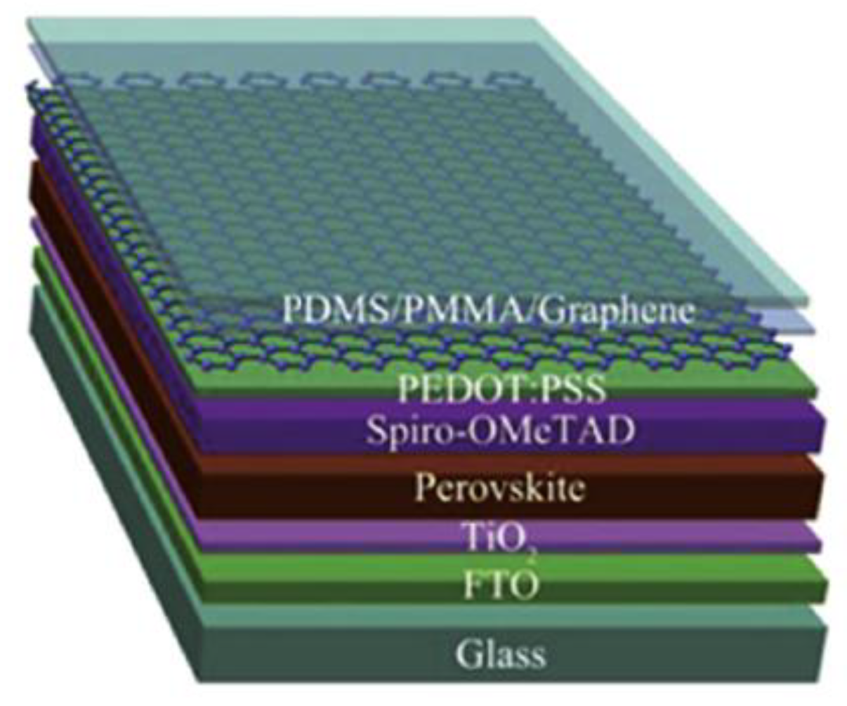
- Hu, X.H.; Jiang, H.; Li, J.; Ma, J.X.; Yang, D.; Liu, Z.K.; Gao, F.; Liu, S.Z. Air and thermally stable perovskite solar cells with CVD-graphene as the blocking layer. Nanoscale 2017, 9, 8274–8280. [Google Scholar] [CrossRef] [PubMed]
- Wang, X.Y.; Li, Z.; Xu, W.J.; Kulkarni, S.A.; Batabyal, S.K.; Zhang, S.; Cao, A.Y.; Wong, L.H. TiO2 nanotube arrays based flexible perovskite solar cells with transparent carbon nanotube electrode. Nano Energy 2015, 11, 728–735. [Google Scholar] [CrossRef]
- Lee, K.T.; Guo, L.; Park, H. Neutral-and multi-colored semitransparent perovskite solar cells. Molecules 2016, 21, 475. [Google Scholar] [CrossRef] [PubMed]
- Hodgkinson, J.L.; Yates, H.M.; Walter, A.; Sacchetto, D.; Moon, S.J.; Nicolay, S. Roll to roll atmospheric pressure plasma enhanced CVD of titania as a step towards the realisation of large area perovskite solar cell technology. J. Mater. Chem. C 2018, 6, 1988–1995. [Google Scholar] [CrossRef]
- Bush, K.A.; Palmstrom, A.F.; Zhengshan, J.Y.; Boccard, M.; Cheacharoen, R.R.; Mailoa, J.P.; McMeekin, D.P.; Hoye, R.L.Z.; Bailie, C.D.; Leijtens, T.; et al. 23.6%-efficient monolithic perovskite/silicon tandem solar cells with improved stability. Nat. Energy 2017, 2, 17009. [Google Scholar] [CrossRef]
- Cheacharoen, R.R.; Rolston, N.; Harwood, D.; Bush, K.A.; Dauskardt, R.H.; McGehee, M.D. Design and understanding of encapsulated perovskite solar cells to withstand temperature cycling. Energy Environ. Sci. 2018, 11, 144–150. [Google Scholar] [CrossRef]
- Tong, G.Q.; Song, Z.H.; Li, C.D.; Zhao, Y.L.; Yu, L.W.; Xu, J.; Jiang, Y.; Sheng, Y.; Shi, Y.; Chen, K.J. Cadmium-doped flexible perovskite solar cells with a low-cost and low-temperature-processed CdS electron transport layer. RSC Adv. 2017, 7, 19457–19463. [Google Scholar] [CrossRef]
- Song, Z.H.; Tong, G.Q.; Li, H.; Li, G.P.; Ma, S.; Liu, Q.; Jiang, Y. Three-dimensional architecture hybrid perovskite solar cells using CdS nanorod arrays as an electron transport layer. Nanotechnology 2017, 29, 025401. [Google Scholar] [CrossRef]
- Ahn, N.; Jeon, I.; Yoon, J.; Kauppinen, E.I.; Matsuo, Y.; Maruyams, S.; Choi, M. Carbon-sandwiched perovskite solar cell. J. Mater. Chem. A 2018, 6, 1382–1389. [Google Scholar] [CrossRef]
- Chen, S.Q.; Wang, J.S.; Zhang, Z.X.; Briscoe, J.; Warwick, M.E.A.; Li, H.Y.; Hu, P. Aerosol assisted chemical vapour deposition of conformal ZnO compact layers for efficient electron transport in perovskite solar cells. Mater. Lett. 2018, 217, 251–254. [Google Scholar] [CrossRef]
- Zhang, Z.X.; Chen, S.Q.; Li, P.P.; Li, H.Y.; Wu, J.S.; Hu, P.; Wang, J.S. Aerosol-assisted chemical vapor deposition of ultra-thin CuOx films as hole transport material for planar perovskite solar cells. Funct. Mater. Lett. 2018, 11, 1850035. [Google Scholar] [CrossRef]


| Device Form | Heating Method (Temperature Range, °C) | Principle Diagram |
|---|---|---|
| Tubular furnace type | Resistance heating mode (~1000) |  |
| Vertical type | Plate heating mode (~500) Induction heating mode (~1200) |  |
| Cylinder type | Induction heating mode (~1200) Infrared radiation heating mode (~1200) |  |
| Tandem surround type | Plate heating mode (~500) Infrared radiation heating mode (~1200) |  |
| Perovskite Material | Pressure | PCE (%) | Ref. |
|---|---|---|---|
| CH3NH3PbI3 | 1 Torr | 14.99 (Mesoscopic) | [54] |
| 15.37 (Planar) | |||
| FAI (Formamidinium iodide) | 2 × 10⁻² Pa | 14.2 | [55] |
| CH3NH3PbI3 | 1 × 10⁻³ Pa | 15.6 | [56] |
| α-FAPbI3 | 10−2 Pa | 12.4 | [57] |
| AMX3 | 10−5–10−6 mbar | ~ | [58] |
| CH3NH3PbBrI3-x | 170 Torr | ~ | [59] |
| CH3NH3I(MAI) | ~ | 16.42 | [60] |
| CH3NH3PbI3 | 10 hPa | ~ | [61] |
| CsPbX3 (X = Cl, Br, I) | 4.8(4.8,5.2) Torr | 5.9 (10.0, 8.3) | [62] |
| (CH3NH3)3Bi2I9 | 10−6 hPa | 0.047 | [63] |
| CH3NH3PbI3 | 104 Pa | ~ | [64] |
| CH3NH3PbI3 | 1 Torr | 7.9 | [65] |
| CsPbBr3 | 150 Pa | ~ | [66] |
| (CH3NH3)3Bi2I9 | 10 hpa | 0.047 | [67] |
| Electrode Material | Device Structures | PCE (%) | Ref. |
|---|---|---|---|
| Graphene CNTS | FET/Graphene/TiO2/PCBM/MAPbI3/Spiro-OMeTAD/CNTs | 11.9 | [101] |
| Graphene | Quartz/graphene/C60/MAPbI3/carbon | 13.93 | [102] |
| Graphene | Glass/graphene/MoO3/PEDOT:PSS/MAPbI3/C60/BCP/LiF/Al | 17.1 | [103] |
| Graphene | PET/ZEOCOAT/graphene/P3HT/MAPbI3/PC71BM/Ag | 11.5 | [104] |
| Graphene | FTO/TiO2/MAPbI3-xClx/Spiro-OMeTAD/PEDOT:PSS/graphene | 12.37 | [105] |
| Graphene | PET/graphene/PEDOT:PSS/MAPbI3/PCBM/Al | 13.94 | [106] |
| Graphene | PEN/graphene/MoO3/PEDOT:PSS/MAPbI3/C60/BCP/LiF/Al | 16.8 | [107] |
| Graphene | PET/graphene/PEDOT:PSS/FAPbI3−xBrx/PCBM/Al | 17.9 | [108] |
| Graphene | Glass or PDMS/graphene/PEDOT:PSS/FAPbI3−xBrx/PCBM/Al | 18.3 | [109] |
| Graphene | FTO/TiO2/MAPbI3/Spiro-OMeTAD/graphene | 6.2 | [110] |
| Graphene | FTO/TiO2/MAPbI3−xClx/Spiro-OMeTAD/PEDOT:PSS/graphene | 11.8 | [111] |
| CNTs | Tifoil/CH3NH3PbI3/TiO2NTs/Spiro-OMeTAD/CNTs | 8.31 | [114] |
| CNTs | Glass/FTO/TiO2/CH3NH3PbI3/CNTs | 3.88 | [115] |
© 2019 by the authors. Licensee MDPI, Basel, Switzerland. This article is an open access article distributed under the terms and conditions of the Creative Commons Attribution (CC BY) license (http://creativecommons.org/licenses/by/4.0/).
Share and Cite
Liu, X.; Cao, L.; Guo, Z.; Li, Y.; Gao, W.; Zhou, L. A Review of Perovskite Photovoltaic Materials’ Synthesis and Applications via Chemical Vapor Deposition Method. Materials 2019, 12, 3304. https://doi.org/10.3390/ma12203304
Liu X, Cao L, Guo Z, Li Y, Gao W, Zhou L. A Review of Perovskite Photovoltaic Materials’ Synthesis and Applications via Chemical Vapor Deposition Method. Materials. 2019; 12(20):3304. https://doi.org/10.3390/ma12203304
Chicago/Turabian StyleLiu, Xia, Lianzhen Cao, Zhen Guo, Yingde Li, Weibo Gao, and Lianqun Zhou. 2019. "A Review of Perovskite Photovoltaic Materials’ Synthesis and Applications via Chemical Vapor Deposition Method" Materials 12, no. 20: 3304. https://doi.org/10.3390/ma12203304
APA StyleLiu, X., Cao, L., Guo, Z., Li, Y., Gao, W., & Zhou, L. (2019). A Review of Perovskite Photovoltaic Materials’ Synthesis and Applications via Chemical Vapor Deposition Method. Materials, 12(20), 3304. https://doi.org/10.3390/ma12203304