Article

Quantifying Joule Heating and Mass Transport in Metal Nanowires during Controlled Electromigration

1
Division of Electrical and Electronic Engineering, Department of Engineering for Future Innovation, Ichinoseki College (Ichinoseki KOSEN), Ichinoseki, Iwate 021-8511, Japan
2
Department of Electrical and Electronic Engineering, Tokyo University of Agriculture and Technology, Koganei, Tokyo 184-8588, Japan
*
Author to whom correspondence should be addressed.
Materials 2019, 12(2), 310; https://doi.org/10.3390/ma12020310
Submission received: 30 December 2018 / Revised: 15 January 2019 / Accepted: 15 January 2019 / Published: 19 January 2019
(This article belongs to the Special Issue Metallic Nanowires and Their Applications)

Abstract

:
The nanoscale heat dissipation (Joule heating) and mass transport during electromigration (EM) have attracted considerable attention in recent years. Here, the EM-driven movement of voids in gold (Au) nanowires of different shapes (width range: 50–300 nm) was directly observed by performing atomic force microscopy. Using the data, we determined the average mass transport rate to be 105 to 106 atoms/s. We investigated the heat dissipation in L-shaped, straight-shaped, and bowtie-shaped nanowires. The maximum Joule heating power of the straight-shaped nanowires was three times that of the bowtie-shaped nanowires, indicating that EM in the latter can be triggered by lower power. Based on the power dissipated by the nanowires, the local temperature during EM was estimated. Both the local temperature and junction voltage of the bowtie-shaped nanowires increased with the decrease in the Joule heating power and current, while the current density remained in the order of 108 A/cm2. The straight-shaped nanowires exhibited the same tendency. The local temperature at each feedback point could be simply estimated using the diffusive heat transport relationship. These results suggest that the EM-driven mass transport can be controlled at temperatures much lower than the melting point of Au.

1. Introduction

The electromigration (EM) phenomenon is of high technological importance for the semiconductor industry, as it is the main cause of failure in integrated circuits [1,2]. The dissipative heating at the interconnect is considered the dominant driving force behind EM, with the cumulative momentum transfer from conduction electrons to thermally activated ions in a conductor. These negative effects can be, if properly tuned, used to our advantage to prepare nanogap electrodes made of metal nanowires for fabricating quantum tunneling devices [3]. This opens the possibility for an alternative method based on only the current passing through a metal nanowire without requiring conventional lithography techniques. However, the EM-generated nanogap procedure with a simple voltage ramp often results in poorly tuned tunnel resistance, which can ultimately destroy the nanowires [3]. To prevent thermal runaway and enable temperature tuning in nanowires, feedback-controlled electromigration (FCE) methods based on resistance/conductance monitoring have been developed [4,5,6,7,8,9]. Although resistance/conductance measurements reflect the structural changes in the nanowires during EM [9], they do not give enough insight into the mechanism of nanogap formation. A real-time imaging of the morphological changes during EM is essential. In our previous studies, the mass transport in electromigrated Au nanowires was investigated using an in situ atomic force microscopy (AFM) technique in ambient air [10]. The established in situ AFM technique helped to better understand the relationship between the wire geometry, current density, and heat dissipation (Joule heating) during FCE. To fabricate functional nanoscale devices such as single-electron transistors [11,12] and single-molecule transistors [13], it is important to quantitatively study the mass transport and local temperature in the nanowires, and better understand the void movements (moving atoms) during EM. Here, we focus on the changes in the morphology of voids in Au nanowires induced by EM, and the local temperature during FCE in Au nanowires observed by performing AFM topography using the diffusive heat transport relationship. Moreover, the effect of the heat dissipation near the nanoconstriction on the nanowire shape is investigated.

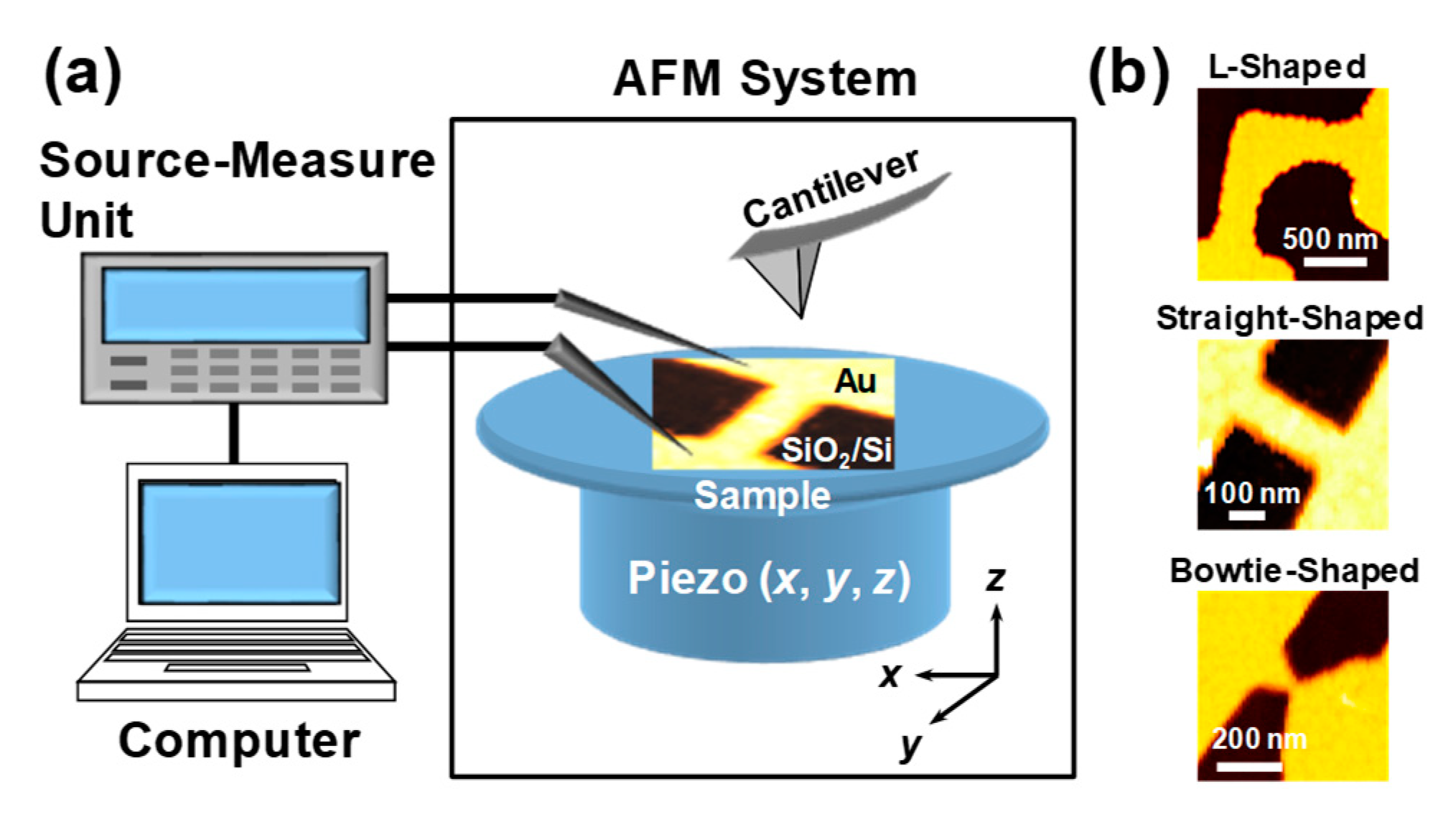
2. Experimental Method

Figure 1a shows the schematic of the experimental setup. The Au nanowires used in this study were defined using electron-beam lithography, evaporation, and lift-off technique on Si/SiO2 substrates. L-shaped, straight-shaped, and bowtie-shaped Au nanowires were fabricated as shown in Figure 1b. The measurements reported in this study were performed in air at room temperature and ambient atmospheric pressure. The morphological modification of the nanowires during FCE was quantitatively evaluated using SPA400/SPI4000 (SII Nanotechnology, Inc., Tokyo, Japan). The AFM measurements were carried out in the contact mode using commercially available silicon nitride cantilevers (Olympus Co., Tokyo, Japan) with a spring constant of 0.02 N/m. The frequency of the scan comprising 256(x) × 128(y) data points was in the range of 5–10 Hz, and the images were obtained in approximately 15–30 s. Each nanowire was placed on a specially designed AFM holder, via which an electric current could be applied through the sample during AFM observation. Here, we focus on the significant structural changes in the nanowires during FCE at the cathode side, due to negligible Joule heating and prominent EM. We captured real-time AFM images of the nanowires from 200 and 500 nm2 topographic scans in the vicinity of the cathode end. It is now generally accepted that the junction resistance RJ is significantly lower than the lead resistance RL. In this case, RJ was approximately in the range of 1–4 Ω, and the overall initial resistance R (=RJ + RL) of the samples was approximately in the range of 33–69 Ω.
A feedback control scheme, which is reported elsewhere [4], was used to apply the electrical stresses to the nanowires. The current–voltage (IV) characteristics of the nanowires were recorded using a computer-controlled source-measure unit (Keithley 2400, Solon, OH, USA). The voltage V applied to the nanowires was automatically increased in constant voltage steps VSTEP, and the conductance G was monitored. When the differential conductance ΔIV reaches the threshold differential conductance GTH, the program reduces the voltage by an amount equal to the feedback (FB) voltage VFB to avoid a catastrophic failure. These voltage reduction events are further referred to as FB points. Subsequently, the voltage ramp was reinitiated continuously.

3. Results and Discussion

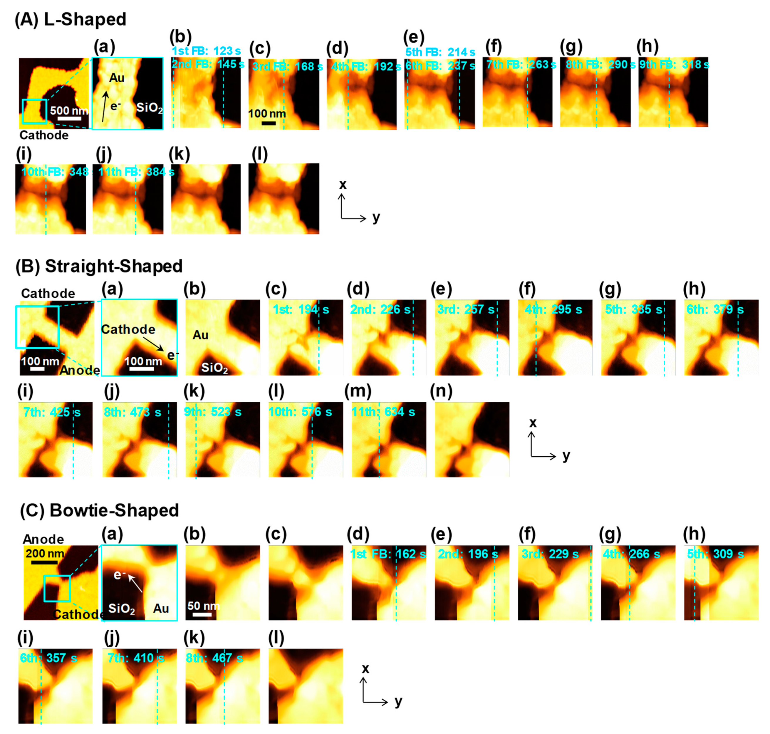
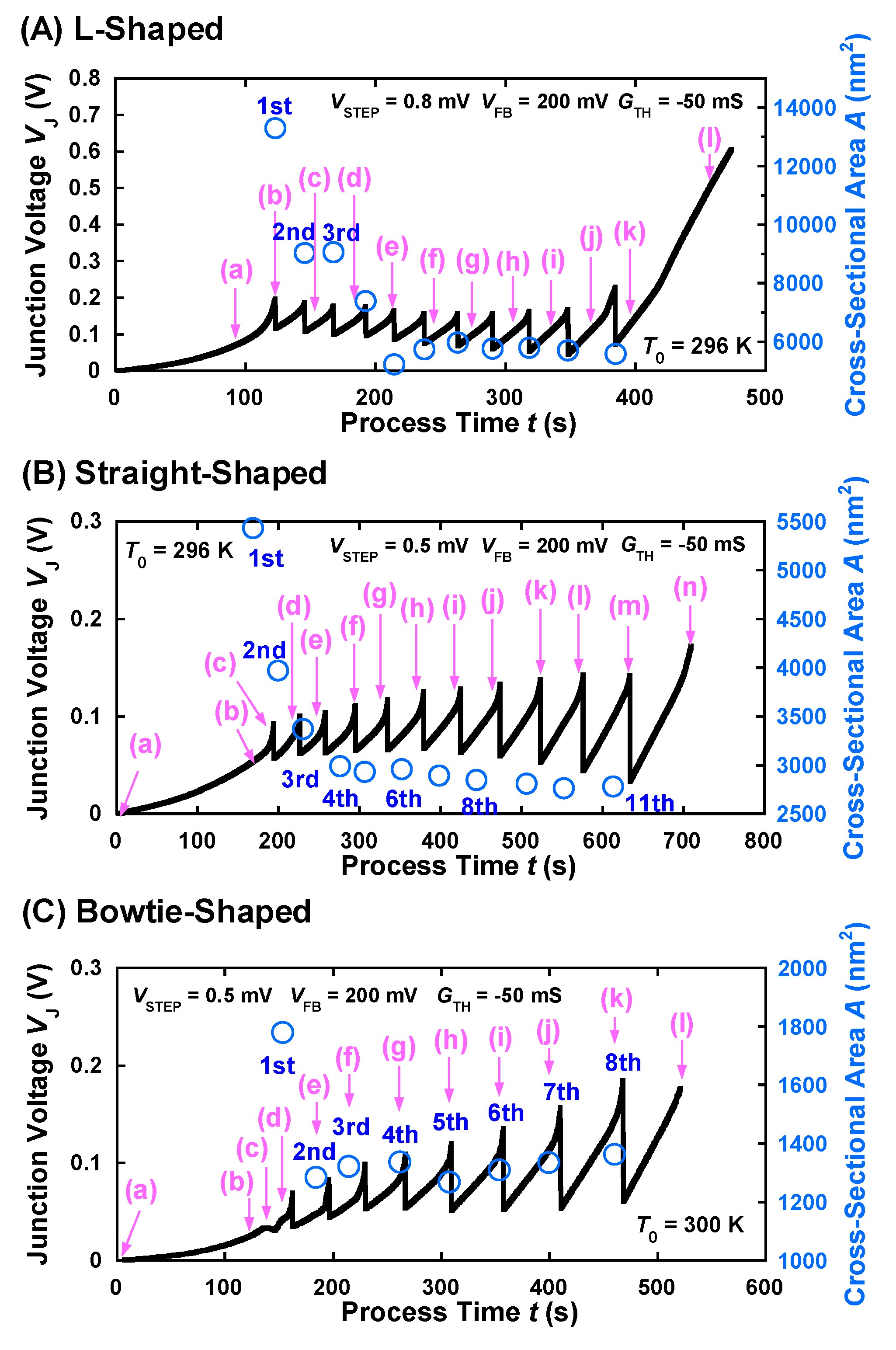
3.1. In Situ AFM Imaging of Au Nanowires during FCE

Figure 2(Aa–l) shows the AFM images of the L-shaped Au nanowires of length 1.5 μm, captured during 92–488 s. The blue dashed lines in Figure 2(Ab–j) indicate the scan positions at each FB point, and the time corresponding to each FB point is indicated in each of the images. The electron flow is from down (cathode) to up (anode). The results show that the structural changes in the nanoconstriction were gradual, and from the 1st to the 11th FB point.
Similar results were obtained for the straight-shaped and bowtie-shaped nanowires of length 300 nm, as shown in Figure 2(Ba–n) and Figure 2(Ca–l), respectively. In Figure 2B, the electrons flow from upper left (cathode) to lower right (anode), whereas in Figure 2C, they move from lower right (cathode) to upper left (anode). Despite different scan directions, in contrast to a direction of electron flow, the EM-induced mass transport in Au nanowires of different shapes was observed in the vicinity of the cathode end, indicating that void movements (moving atoms) during EM did not suffer from the scan of the cantilever. Figure 3A shows the time evolutions of the junction voltage VJ and the cross-sectional area A of the L-shaped nanowires during the FCE process for VSTEP = 0.8 mV, VFB = 200 mV, and GTH = −50 mS. The starting points of the scans, shown in Figure 2(Aa–l), are indicated using pink arrows, as shown in Figure 3A. To calculate A from the AFM images of the nanowire, the SiO2 surface observed in the images was used. The cross sections perpendicular to the direction of electron flow were taken near the nanoconstriction. Each open circle represents the A value of the image including the automatic decrease in the voltage by VFB. There was a decrease in A from 13,310 nm2 (1st FB point) to 5597 nm2 (11th FB point) during the voltage feedback process, indicating that the FCE process thinned down the nanowire without any thermal runaway or melting.
Similarly, Figure 3B,C shows the time evolutions of VJ and A of the straight-shaped and bowtie-shaped nanowires, respectively, during the FCE process for VSTEP = 0.5 mV, VFB = 200 mV, and GTH = −50 mS. The pink arrows, indicated in Figure 3B,C, correspond to the starting points of the scans shown in Figure 2(Ba–n) and Figure 2(Ca–l), respectively. As shown in Figure 3B, A of the straight-shaped nanowires reduced from 5437 nm2 (1st FB point) to 2996 nm2 (4th FB point) and gradually decreased to 2766 nm2 (11th FB point). Figure 3C shows the gradual decrease in A of the bowtie-shaped nanowires, from 1781 to 1271 nm2. The VJA characteristics confirm that the rapid EM of the Au atoms was suppressed under the feedback algorithm. Figure 4a–c shows the current density j of the L-shaped, straight-shaped, and bowtie-shaped nanowires as a function of the FCE process time. Notably, despite the different shapes of the nanowires, the value j (obtained by dividing I by A) remains constant, in the order of 108 A/cm2 during the FCE process. The roughly estimated j value is reasonably consistent with previous reports on the failure of the current density of Au nanowires [6,7,14,15].

3.2. Mass Transport in Electromigrated Au Nanowires

The quantitative mass transport used to characterize the EM process in the nanowires can be obtained from the measured nanowire topographies. We defined the SiO2 surface observed in the images as the reference plane. The Au mass transport was calculated by summing the differential volumes in the vicinity of the cathode side, before and after the FB point during the FCE process, and then multiplying the result with the Au density [10]. The change in the volume between the images can be expressed as follows:
Δ U ab ( nm 3 ) = x , y ( f axy Δ S a f bxy Δ S b )
where a and b are the image indices, x and y are the positions in the image, ΔSa (=ΔSb) (nm2) is the total area of the image (nm2)/(256 × 128 data points), and faxy and fbxy (nm) are the heights of the points with respect to the reference plane. The Au mass ΔMab transported from the cathode can be expressed as follows.
Δ M ab ( atoms ) = Δ U ab ( nm 3 ) × d   ( atoms / nm 3 )
where d is the atom density (=58.9 atoms/nm3) [16], assuming that the Au nanowire has an FCC structure. We determined the rate of mass transport ΔRab in time intervals of 30 s between two AFM images. Finally, the average values ΔMAVE and ΔRAVE of ΔMab and ΔRab were obtained, as listed in Table 1. The average values (ΔRAVE) of the mass transport rate were in reasonable agreement with the values reported for real-time TEM imaging of EM-induced nanogap formation, that is, 106 atoms/s (=105 atoms/50 ms) [17]. The straight-shaped and bowtie-shaped nanowires had relatively lower ΔRAVE values than the L-shaped nanowire. The relatively low ΔRAVE could be a result of the smaller cross-sectional area A and lower constant voltage step VSTEP. To investigate the influence of the temperature (due to the Joule heating) required to control the lower mass transport, we first used the constant power model for the three nanowires.

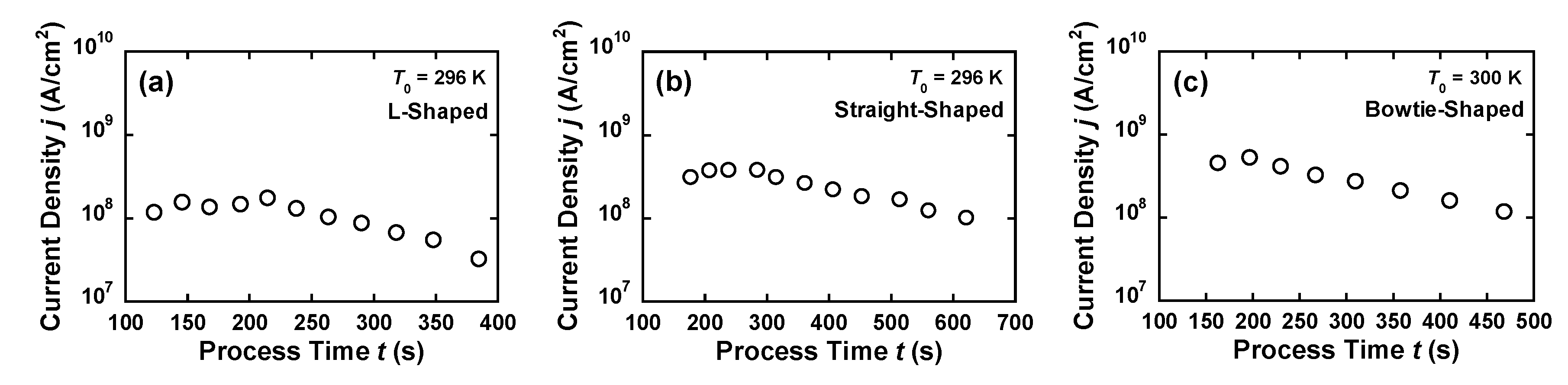
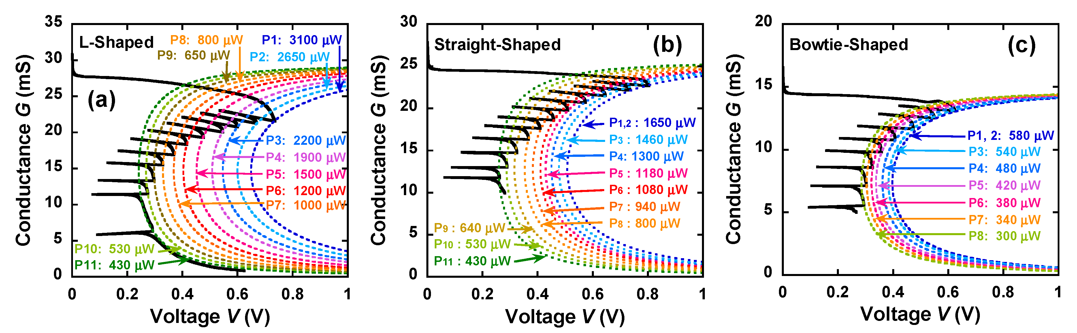
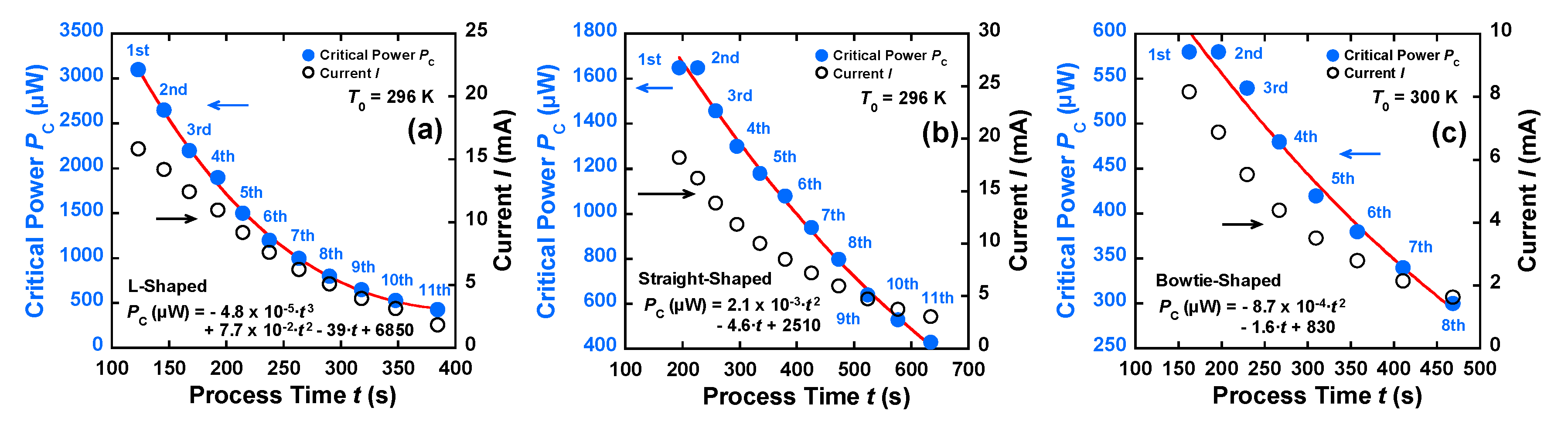
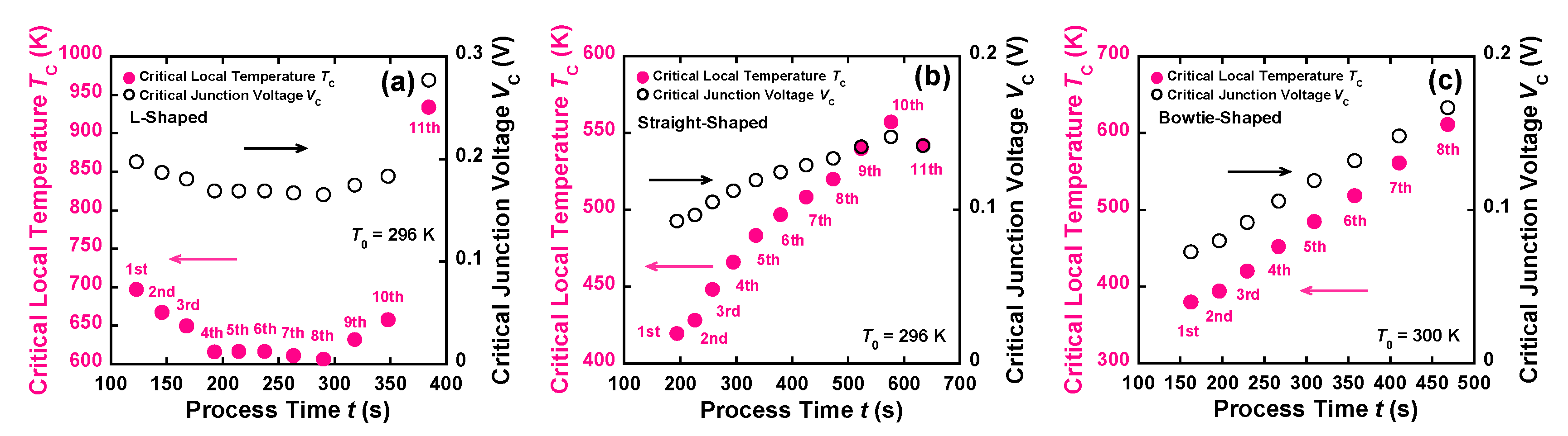
3.3. Nanoscale Heat Dissipation in Electromigrated Au Nanowires

The overall curve with some FB points can be modeled using the following equation [4,6]:
V = V J + V L = P J I + R L I
where V is the total voltage applied to the device, VJ and VL [V] are the voltages across the constriction and leads, respectively, PJ (μW) is the power dissipated at the nanoconstriction, and I (mA) is the current. The curves shown in Figure 5a–c represent the fit of Equation (3) to the GV characteristics of the nanowires during the FCE process. PJ at each FB point was defined as the critical power PC. PC was fitted to the model and was found to decrease from 1650 μW (at the first and second FB points) to 430 μW (at the 11th FB point) for the straight-shaped nanowires, shown in Figure 5b, and from 580 μW (at the first and second FB points) to 300 μW (at the 8th FB point) for the bowtie-shaped nanowires, shown in Figure 5c. For the L-shaped nanowires shown in Figure 5a PC ranged from 3100 μW (at the first FB point) to 430 μW (at the 11th FB point). Figure 6a–c shows the PC and I values as a function of the FCE process time. The red lines in Figure 6a–c indicate the fitting result of PC. PC reduced with the decrease in I, which is consistent with previous reports [9,18]. The smaller the nanoconstriction, the lower the critical power consumed during the FCE process. The tapered region in the bowtie-shaped nanowires may allow easy flow of Joule heating generated in the nanoconstriction. Thinner and narrower wires—particularly ones made of Au—are known to generate lower heat when the electron–phonon scattering length is on the order of 170 nm [15]. Thus, the mass transport can be precisely tuned using a lower Joule heating power. For metallic constrictions in the diffusive regime, the scale of the voltage due to the constriction resistance is associated with the temperature scale [6,19].
T 2 = T 0 2 + V J 2 4 L
where L (V2/K2) (=(π2/3)(k/e)2) is the Lorenz number, and T and T0 (K) are the temperatures of the constriction and its environment, respectively. This relationship can be theoretically deduced, assuming that the electrical conductivity is related to the thermal conductivity (Wiedemann–Franz law) [6,19]. In this study, at the onset of EM, the local temperature T at the constriction was defined as the critical local temperature TC, and VJ was defined as the critical junction voltage VC. Thus, at each FB point, VC could be calculated with respect to the time evolution by dividing PC by I. When T at the constriction is equal to TC, TC at each FB point can be simply estimated using the diffusive heat transport relationship as follows [6,19]:
T C = T 0 2 + V C 2 4 L = T 0 2 + P C 2 4 I 2 L
According to Equation (5), TC depends on VC. Figure 7a–c shows the time evolutions of TC and VC under the feedback algorithm. Table 2 presents the relationship between TC, VC, PC, and I, demonstrating the range of electrical and thermal properties at the FB points of the three nanowires. The TC value of the bowtie-shaped nanowires increased from 379 to 612 K at T0 = 300 K with the increase in VC from 0.073 to 0.17 V. Both TC and VC linearly varied with the decrease in PC and I. This tendency was quite similar to that exhibited by the straight-shaped nanowires. The estimated values were in reasonable agreement with previous reports (325–660 K) [7,8,9,14,20,21]. In the case of the L-shaped nanowires, although TC decreased from 697 K (at the 1st FB point) to 611 K (at the 7th FB point), TC increased from 607 K (at the 8th FB point) to 935 K (at the 11th FB point) in the same manner as that observed for the straight-shaped and bowtie-shaped nanowires. This implies that the longer and wider L-shaped nanowires consumed more power to approximately the 7th FB point, whereas the behavior of the narrower L-shaped nanowires was similar to the behavior of the straight-shaped and bowtie-shaped nanowires after approximately the 7th FB point. The higher value of TC at the 11th FB point could have been due to the accumulation of Joule heating for a long time between the 10th and 11th FB points. As shown in Figure 2(Al), at the end of the FCE process, there was no abrupt failure of the nanoconstriction due to melting, because the local temperature was significantly lower than the melting point of gold (~1337 K) [22]. The TC values at each FB point could be roughly interpreted using the diffusive heat transport relationship, and the value of TC at the 1st FB point was related to the wire size. These results confirm the EM-induced mass transport phenomenon in Au nanowires from room temperature to temperatures significantly lower than the melting point of Au, with TC increasing in a controlled manner independent of the nanowire shape.

4. Conclusions

We studied the mass transport and local Joule heating in Au nanowires during EM in real-time by performing AFM in air at room temperature and ambient atmospheric pressure. The applied voltage and current measurements and cross-sectional area of the nanoconstriction obtained during FCE indicated that the EM-induced mass transport proceeded in the order of 108 A/cm2 in a gradual manner under the application of a voltage feedback algorithm. The estimated average mass transport was in the order of 105 to 106 atoms/s; the straight-shaped and bowtie-shaped nanowires gave lower values. Furthermore, based on the power dissipated by the nanowires, we found that the local temperature in the nanoconstriction during FCE ranged from room temperature to temperatures lower than the melting point of Au. The results suggest that the accumulation and movement of the voids were induced by EM without any melting of the large parts of the nanowires due to Joule heating. Moreover, the control of the mass transport during EM hardly depended on the shape of the nanowires. The results of this study are expected to provide more insight into the matter of fluxes during EM. The technological implications of this work are that if bowtie-shaped nanowires are used to prepare nanogap electrodes, then in order to control and observe lower mass transport, they must be as narrow as possible, while remaining as short as possible.

Author Contributions

Conceptualization, J.-i.S.; Data curation, M.Y.; Formal analysis, M.Y.; Funding acquisition, J.-i.S.; Investigation, M.Y.; Methodology, M.Y.; Project administration, J.-i.S.; Resources, J.-i.S.; Supervision, J.-i.S.; Validation, M.Y.; Writing—original draft, M.Y.; Writing—review & editing, J.-i.S.

Conflicts of Interest

The authors declare no conflict of interest.

References

  1. Blech, I.A.; Meieran, E.S. Direct transmission electron microscope observation of electrotransport in aluminum thin films. Appl. Phys. Lett. 1967, 11, 263–266. [Google Scholar] [CrossRef]
  2. Ho, P.S.; Kwok, T. Electromigration in metals. Rep. Prog. Phys. 1989, 52, 301–348. [Google Scholar] [CrossRef]
  3. Park, H.; Lim, A.K.L.; Alivisatos, A.P.; Park, J.; McEuen, P.L. Fabrication of metallic electrodes with nanometer separation by electromigration. Appl. Phys. Lett. 1999, 75, 301–303. [Google Scholar] [CrossRef]
  4. Strachan, D.R.; Smith, D.E.; Johnston, D.E.; Park, T.-H.; Therien, M.J.; Bonnell, D.A.; Johnson, A.T. Controlled fabrication of nanogaps in ambient environment for molecular electronics. Appl. Phys. Lett. 2005, 86, 043109. [Google Scholar] [CrossRef] [Green Version]
  5. Esen, G.; Fuhrer, M.S. Temperature control of electromigration to form gold nanogap junctions. Appl. Phys. Lett. 2005, 87, 263101. [Google Scholar] [CrossRef]
  6. Hoffmann, R.; Weissenberger, D.; Hawecker, J.; Stöffler, D. Conductance of gold nanojunctions thinned by electromigration. Appl. Phys. Lett. 2008, 93, 043118. [Google Scholar] [CrossRef]
  7. Xiang, A.; Hou, S.; Liao, J. Tuning the local temperature during feedback controlled electromigration in gold nanowires. Appl. Phys. Lett. 2014, 104, 223113. [Google Scholar] [CrossRef]
  8. Jeong, W.; Kim, K.; Kim, Y.; Lee, W.; Reddy, P. Characterization of nanoscale temperature fields during electromigration of nanowires. Sci. Rep. 2014, 4, 4975. [Google Scholar] [CrossRef]
  9. Wu, Z.M.; Steinacher, M.; Huber, R.; Calame, M.; van der Molen, S.J.; Schönenberger, C. Feedback controlled electromigration in four-terminal nanojunctions. Appl. Phys. Lett. 2007, 91, 053118. [Google Scholar] [CrossRef] [Green Version]
  10. Yagi, M.; Saito, T.; Shirakashi, J. In situ atomic force microscopy imaging of structural changes in metal nanowires during feedback-controlled electromigration. J. Vac. Sci. Technol. B 2015, 33, 051806. [Google Scholar] [CrossRef]
  11. Bolotin, K.I.; Kuemmeth, F.; Pasupathy, A.N.; Ralph, D.C. Metal-nanoparticle single-electron transistors fabricated using electromigration. Appl. Phys. Lett. 2004, 84, 3154–3156. [Google Scholar] [CrossRef]
  12. Arzubiaga, L.; Golmar, F.; Llopis, R.; Casanova, F.; Hueso, L.E. In situ electrical characterization of palladium-based single electron transistors made by electromigration technique. AIP Adv. 2014, 4, 117126. [Google Scholar] [CrossRef] [Green Version]
  13. Liang, W.; Shores, M.P.; Bockrath, M.; Long, J.R.; Park, H. Kondo resonance in a single-molecule transistor. Nature 2002, 417, 725–729. [Google Scholar] [CrossRef] [PubMed]
  14. Campbell, J.M.; Knobel, R.G. Feedback-controlled electromigration for the fabrication of point contacts. Appl. Phys. Lett. 2013, 102, 023105. [Google Scholar] [CrossRef] [Green Version]
  15. Durkan, C.; Schneider, M.A.; Welland, M.E. Analysis of failure mechanisms in electrically stressed Au nanowires. J. Appl. Phys. 1999, 86, 1280–1286. [Google Scholar] [CrossRef]
  16. Popescu, R.; Müller, E.; Wanner, M.; Gerthsen, D.; Schowalter, M.; Rosenauer, A.; Böttcher, A.; Löffler, D.; Weis, P. Increase of the mean inner Coulomb potential in Au clusters induced by surface tension and its implication for electron scattering. Phys. Rev. B 2007, 76, 235411. [Google Scholar] [CrossRef]
  17. Heersche, H.B.; Lientschnig, G.; O’Neill, K.; van der Zant, H.S.J.; Zandbergen, H.W. In situ imaging of electromigration-induced nanogap formation by transmission electron microscopy. Appl. Phys. Lett. 2007, 91, 072107. [Google Scholar] [CrossRef] [Green Version]
  18. Stöffler, D.; Fostner, S.; Grütter, P.; Hoffmann-Vogel, R. Scanning probe microscopy imaging of metallic nanocontacts. Phys. Rev. B 2012, 85, 033404. [Google Scholar] [CrossRef]
  19. Chen, T.Y.; Chien, C.L.; Manno, M.; Wang, L.; Leighton, C. Ballistic heat transport in nanocontacts. Phys. Rev. B 2010, 81, 020301. [Google Scholar] [CrossRef]
  20. Trouwborst, M.L.; van der Molen, S.J.; van Wees, B.J. The role of Joule heating in the formation of nanogaps by electromigration. J. Appl. Phys. 2006, 99, 114316. [Google Scholar] [CrossRef] [Green Version]
  21. Taychatanapat, T.; Bolotin, K.I.; Kuemmeth, F.; Ralph, D.C. Imaging electromigration during the formation of break junctions. Nano Lett. 2007, 7, 652–656. [Google Scholar] [CrossRef] [PubMed]
  22. Haynes, W.M. CRC Handbook of Chemistry and Physics, 90th ed.; CRC Press, Taylor & Francis Group: Boca Raton, FL, USA, 2009; pp. 12–203. [Google Scholar]
Figure 1. (a) Schematic of the experimental setup for in situ atomic force microscopy (AFM) imaging; (b) AFM images of Au nanowires of different shapes.
Materials 12 00310 g001
Figure 2. (A) Atomic force microscopy (AFM) images of the L-shaped nanowires captured with a scanning window of 500 × 500 nm2. The images were captured during the following time intervals: (a) t = 92–122 s, (b) t = 122–153 s, (c) t = 153–183 s, (d) t = 183–213 s, (e) t = 213–244 s, (f) t = 244–274 s, (g) t = 274–305 s, (h) t = 305–335 s, (i) t = 335–366 s, (j) t = 366–396 s, (k) t = 396–427 s, and (l) t = 457–488 s. The light-blue dashed lines in (bj) indicate each scan line from the 1st to the 11th corresponding feedback (FB) point. The time indicated at the top of each image is the time corresponding to each FB point. (B) AFM images of the straight-shaped nanowires captured with a scanning window of 300 × 300 nm2. The images were captured during the following time intervals: (a) t = 0–15 s, (b) t = 168–184 s, (c) t = 184–199 s, (d) t = 214–230 s, (e) t = 245–260 s, (f) t = 291–306 s, (g) t = 322–337 s, (h) t = 368–383 s, (i) t = 414–429 s, (j) t = 460–475 s, (k) t = 521–536 s, (l) t = 567–582 s, (m) t = 628–644 s, and (n) t = 705–720 s. The light-blue dashed lines in (cm) indicate each scan line from the 1st to the 11th corresponding FB point. The time indicated at the top of each image is the time corresponding to each FB point. (C) AFM images of the bowtie-shaped nanowires captured with the scanning window of 200 × 200 nm2. The images were captured during the following time intervals: (a) t = 0–15 s, (b) t = 122–138 s, (c) t = 138–153 s, (d) t = 153–168 s, (e) t = 184–199 s, (f) t = 214–230 s, (g) t = 261–276 s, (h) t = 307–322 s, (i) t = 353–368 s, (j) t = 399–414 s, (k) t = 460–475 s, (l) t = 521–537 s. The light-blue dashed lines in (dk) indicate each scan line from the 1st to the 8th corresponding FB point. The time indicated at the top of each image corresponds to the time of each FB point.
Materials 12 00310 g002
Figure 3. Time evolution of the VJA characteristics of the (A) L-shaped, (B) straight-shaped, and (C) bowtie-shaped nanowires during feedback-controlled electromigration (FCE).
Materials 12 00310 g003
Figure 4. Current densities of the (a) L-shaped, (b) straight-shaped, and (c) bowtie-shaped nanowires as a function of the FCE process time.
Materials 12 00310 g004
Figure 5. G as a function of the total voltage V for the (a) L-shaped, (b) straight-shaped, and (c) bowtie-shaped nanowires during FCE. The dashed lines indicate the fitting results of the Joule heating model.
Materials 12 00310 g005
Figure 6. Time evolution of the PCI characteristics of the (a) L-shaped, (b) straight-shaped, and (c) bowtie-shaped nanowires as a function of the FCE process time. The red lines indicate the fitting result of PC (μW): (a) −4.8 × 10⁻⁵·t3 + 7.7 × 10⁻²·t2 − 39·t + 6850 (R = 0.999), (b) 2.1 × 10⁻³·t2 − 4.6·t + 2510 (R = 0.997), and (c) −8.7 × 10⁻⁴·t2 − 1.6·t + 830 (R = 0.991).
Materials 12 00310 g006
Figure 7. Time evolution of the TCVC characteristics of the (a) L-shaped, (b) straight-shaped, and (c) bowtie-shaped nanowires as a function of the FCE process time.
Materials 12 00310 g007
Table 1. FB parameters, average mass transport values, and average rates of mass transport for each Au nanowire.
NanowireVSTEP (mV)VFB (mV)GTH (mS)ΔMAVE (atoms)ΔRAVE (atoms/s)
L-Shaped0.8200−502.3 × 1077.6 × 105
Straight-Shaped0.5200−502.3 × 1067.7 × 104
Bowtie-Shaped0.5200−502.0 × 1066.6 × 104
Table 2. Critical parameter ranges for the L-shaped, straight-shaped, and bowtie-shaped nanowires.
NanowireI (mA)PC (µW)VC (V)TC (K)
L-Shaped1.84–15.9430–31000.17–0.28607–935
Straight-Shaped3.08–18.2430–16500.093–0.15420–557
Bowtie-Shaped1.63–8.16300–5800.073–0.17379–612

